
 Open Access Article
 This Open Access Article is licensed under a Creative Commons Attribution-Non Commercial 3.0 Unported Licence
Efficient and chromaticity-stable flexible white organic light-emitting devices based on organic–inorganic hybrid color-conversion electrodes†
Cuiyun Peng‡
a,
Kangping Liu‡b,
Shuanglong Wangb,
Nanjie Yuc,
Zhenyu Tangb,
Zhitian Lingb,
Hong Lianb,
Guo Chen*b,
Yingjie Liaob,
Weixia Lana and
Bin Wei *a
*a
aSchool of Mechatronic Engineering and Automation, Shanghai University, 149 Yanchang Road, Shanghai, 200072, P. R. China. E-mail: bwei@shu.edu.cn
bKey Laboratory of Advanced Display and System Applications, Ministry of Education, Shanghai University, 149 Yanchang Road, Shanghai, 200072, P. R. China. E-mail: chenguo@shu.edu.cn
cDepartment of Electrical and Computer Engineering, University of Illinois at Urbana-Champaign, 306 N. Wright St., Urbana, Illinois 61801, USA
First published on 22nd July 2019
Abstract
We have developed a novel organic–inorganic hybrid color conversion electrode composed of Ag NWs/poly[2-methoxy-5-(2-ethylhexyloxy)-1,4-phenylenevinylene] (MEH-PPV) via a solution process, which is the first report on a color conversion electrode for applications in flexible optoelectronics. Using the Ag NWs/MEH-PPV composite film as the anode on polyethylene terephthalate substrate and combined with a blue organic light emitting devices (OLEDs) unit employing bis(3,5-difluoro-2-(2-pyridyl)phenyl-(2-carboxypyridyl)iridium(III)) (Flrpic) in 1,3-bis(carbazol-9-yl)benzene (mCP) as the emitting layer, a highly efficient and chromaticity-stable color-conversion flexible white OLEDs (WOLEDs) is achieved with a maximum current efficiency of 20.5 cd A−1. To the best of our knowledge, this is the highest efficiency reported for color-conversion based flexible WOLEDs. Our work provides an approach to achieving high-performance flexible WOLEDs devices and demonstrates great potential for lighting and display applications.
1. Introduction
The high-efficiency organic light-emitting devices (OLEDs) have attracted significant interests for next-generation solid-state lighting and display applications.1–3 Theoretically, white OLEDs (WOLEDs) can be simply obtained by additive mixing of three primary organic emitting layers or two complementary colors.4,5 In general, the fabrication of WOLEDs usually employs a single emissive layer doped simultaneously with different color dopants, or vertical stacking of several single OLED units structures with different colors emissions.6 Although highly efficient WOLEDs have been achieved by using these methods, these WOLEDs often deteriorate from serious color shift over time due to the time-dependent EL spectra along with the varying voltages and the carrier recombination zone shift. Moreover, the luminogens doping concentration should be carefully tuned to realize a balanced exciton distribution profile among the emissive layers, which contends against the low cost requirement in general applications.7,8 These disadvantages could be remedied by combining single blue OLEDs and a color conversion layer (CCL) to simplify the fabrication process and achieve high color stability.9 In this scheme, the CCL can absorb photons originated from the blue EL and consequently the blue photons are down-converted to longer-wavelength colors, generating white light emission through mixing with the redundant and unconverted blue photons. OLED devices with a single blue emitter in this so-called down-conversion scheme are essentially monochromatic which can avoid energy transferring from various band gap emitters and color shifts that result from the complexity of mixed different colors in a single device.10On the other hand, the high-performance conductive films are a crucial component of the flexible WOLEDs and a variety of other optoelectronic devices, as a high-performance flexible conductor will be required to enlarge these devices from the lab scale to the commercial scale.11 The most commonly used flexible conducting materials are primarily sputtered indium tin oxide (ITO) with excellent electrical and optical properties. However, several crucial drawbacks, such as the high cost, the limited reserves of indium and the brittle nature hinder its sustainable applications in flexible electronics in the future.12,13 With the emerging and rapid development of flexible organic electronics, great efforts have been made to develop alternative conductors with high flexibility including conducting polymers, metal nanowires, metal meshes, carbon nanotubes, graphene and even graphite.14–17 Among them, silver nanowires (Ag NWs) film are an appealing candidate because of their superior features such as desirable transparent property, excellent flexibility and low sheet resistance.18 Very recently, our group demonstrated a high-performance all-solution-processable flexible organic solar cells based on opaque graphite bottom cathode and a transparent silver nanowires (Ag NWs) top anode.19 However, the performance of Ag NWs percolation networks is still not as good as ITO and there are still addressed disadvantages that inhibit the commercial application of Ag NWs as the electrodes in flexible electronics due to their high peaks created by overlapping junctions, poor adhesion between the Ag NWs and substrate and relatively large contact resistance.20
To overcome these drawbacks, various methods have been proposed. Gaynor et al. applied a flat-plate press to embed the nanowires into the polymer, demonstrating a solution-processed Ag nanowire/poly(methyl methacrylate) composite electrode with improved electrical conductivity and roughness and achieving an efficient flexible WOLEDs.21 Lian et al. developed an effective flexible conductive film for OLEDs by embedding Ag NWs into a non-conducting poly(vinylalcohol) to form highly smooth, conductive, and uniform composite electrode.22 However, the above methods require an excessively thick polymer supporting layer, which may lead to an increased driving voltage and/or electron–hole imbalance due to the low conductivity and transparency of the polymers, thus deteriorating the device performance. Although recent demonstrations use transparent conductive materials such as PEDOT:PSS or a buffer layer to overcoat the Ag NWs to reduce the surface roughness, these methods are usually complex and need additional materials, which increases the cost of the electrode.23,24
In this study, we report a solution-processed Ag NWs/poly[2-methoxy-5-(2-ethylhexyloxy)-1,4-phenylenevinylene] (MEH-PPV) color conversion electrode for high-efficiency flexible WOLEDs. An efficient hot-pressing method is utilized to improve the conductivity and smoothness of the Ag NWs/MEH-PPV composite film. The parameters of hot-pressing are carefully adjusted to get an optimum result in terms of conductivity and roughness. The hot-pressed Ag NWs/MEH-PPV color conversion electrode with a low sheet resistance of 21.8 Ω sq−1 and a smooth surface is fabricated, which obviously satisfies the requirements of flexible optoelectronic devices. Highly efficient and chromaticity-stable flexible WOLEDs were implemented based on the Ag NWs/MEH-PPV color conversion anode.
2. Experimental section
2.1 General information
MEH-PPV was purchased from Luminescence Technology Corp (China). Ag NWs solution was purchased from BlueNano Company (Cornelius, NC, USA), with an average diameter of 80 nm and length of 30 μm. The other organic functional materials were obtained from e-Ray Optoelectronics Corp. (Taipei, Taiwan). Polyethylene terephthalate (PET) substrates were ordered from CSG Holding Co. Ltd (China). All chemicals and regents in this work were used as received from commercial sources without further treatment unless otherwise stated.2.2 Preparation of Ag NWs/MEH-PPV electrode
The Ag NWs/MEH-PPV color conversion electrodes were prepared by a successive spin-coating process on precleaned PET substrates. To fabricate the composite film, the PET substrates were cleaned by detergent, de-ionized water, and isopropanol. Ag NWs suspension was spin-coated onto the substrate in air, which was then annealed at 100 °C for 15 min. Subsequently, the Ag NWs film was hot-pressed by a self-designed compressor controlled by compressed air. The pressure intensity applied on the samples can be tuned by adjusting the pressure of compressed air. The Ag NWs film was covered between two clean glass substrates edge to edge, which ensures a smooth and clean contact. And then transferred into the compressor and applied different temperature, pressure and duration to obtain the optimum parameters. Later, MEH-PPV solution was spin-coated on the bottom Ag NWs layer in a glovebox, followed by drying at 60 °C for 15 min. The thickness of the MEH-PPV CCL was controlled by adjusting the concentration of the solution.2.3 Device fabrication
The substrate coated with Ag NWs/MEH-PPV color conversion electrode was transferred into a high-vacuum system with a base pressure of 5 × 10⁻⁶ mbar for the following OLED fabrication. The devices structure of the evaporated flexible WOLEDs (Devices W1, W2 and W3) followed as: Ag NWs/MEH-PPV (λ nm)/TAPC (40 nm)/TCTA (10 nm)/mCP:15%Flrpic (20 nm)/B3PYMPM (50 nm)/Liq (0.8 nm)/Al (200 nm), where λ are 100, 160 and 200 nm, respectively, as shown in Fig. 1a and b. TCTA (4,4′,4′′-tris(carbazol-9-yl)triphenylamine) and TCTA (4,4′,4′′-tris(carbazol-9-yl)triphenylamine) serves as hole transporting layer. mCP (1,3-bis(carbazol-9-yl)benzene) is the blue host material. Flrpic (bis(3,5-difluoro-2-(2-pyridyl)phenyl-(2-carboxypyridyl)iridium(III))) is the blue phosphorescent guest material. B3PYMPM (4,6-bis(3,5-di(pyridin-3-yl)phenyl)-2-methylpyrimidine) is electron transporting layer. Liq (8-hydroxyquinolinolato-lithium) and Al are electron injection layer and cathode, respectively. Chemical structures of the emitting materials described in the OLEDs devices are shown in Fig. 1c. Organic layers and a metal cathode layer were evaporated successively by using shadow masks. The entire organic layers and the Al cathode were deposited without exposure to the atmosphere, by which OLEDs with an active areas of 4 mm2 were obtained. The deposition rates for the organic materials and Al were typically 1.0 and 5.0 Å s−1, respectively. The layer thickness was controlled in situ using a quartz crystal monitor.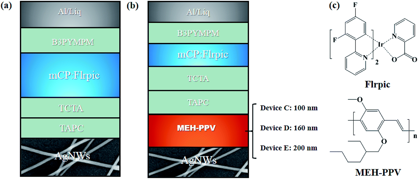 | ||
| Fig. 1 Schematic structures of the tested flexible (a) blue and (b) white devices with different substrates electrode based on the Ag NWs architecture. (c) Chemical structures of the emitting materials Flrpic and MEH-PPV. | ||
2.4 Characterization
The surface morphology of the Ag NWs coated on the PET substrate was investigated by the atomic force microscope (AFM) technique in contact mode using the Seiko instrument SPA 400 AFM system. The sheet resistance is tested with a four-point probe. The transmittance of Ag NWs electrode and absorption spectra of MEH-PPV CCL was measured with an ultraviolet-visible-near infrared spectrophotometer (U-3900H, Hitachi). Photoluminescent spectra of MEH-PPV were tested on an Edinburgh Instruments Ltd (FLSP920) fluorescence spectrophotometer in the solid state. The current–voltage–luminescence characteristics were measured by a Keithley 2400 source meter and a PR-650 Spectra Colorimeter. The luminance and spectra of each device were measured in the direction perpendicular to the substrate.3. Results and discussion
3.1 Optical and electrical properties of Ag NWs/MEH-PPV composite film
The transmittance within the visible range and conductivity are two key parameters for transparent conductive electrode. To determine the optimum conditions, the optical transmittance and sheet resistance of Ag NWs electrode with different suspension concentration (3, 4, 5, 8 and 10 mg mL−1) are studied and the results are shown in Fig. 2a. When the concentration for Ag NWs solution increased from 3 mg mL−1 to 10 mg mL−1, the transmittance of the three samples slightly decreased from 89.8% to 59.5%, respectively. And the change of the sheet resistance shows the similar trend. Here, the figure of merit (ϕFOM) is used to characterize the optical and electrical properties of the samples simultaneously, which is defined as follows:25Tav is the average transmittance in the visible light range and Rsh is the sheet resistance. For the resulting Ag NWs electrode, its figure of merit first increases then decreases with increasing Ag NWs concentration from 3 mg mL−1. Comparing the ϕFOM values, ϕFOM (3 mg mL−1) = 7.12 × 10⁻³, ϕFOM (4 mg mL−1) = 7.90 × 10⁻³, ϕFOM (5 mg mL−1) = 3.31 × 10⁻³, ϕFOM (8 mg mL−1) = 2.73 × 10⁻³ and ϕFOM (10 mg mL−1) = 1.71 × 10⁻³. Thus, the Ag NWs film with the concentration of 4 mg mL−1 performs the best, which is chosen as the optimum (Fig. 2b).
 | ||
| Fig. 2 (a) Sheet resistance (black line) and transmittance (red line) versus the various concentration of Ag NWs suspension and (b) the corresponding figure of merit versus the concentration of Ag NWs suspension. | ||
Mechanical pressure applied on the Ag NWs/MEH-PPV composite film with different temperatures and durations are studied. Here, Rχ = (R − R0)/R0 is used to characterize the changes of Rsh for the Ag NWs/MEH-PPV film during hot pressing process, where R0 and R are the sheet resistances before and after hot pressing.26 Fig. 3a and b demonstrates the variation of Rsh and root mean square (RMS) under a pressure from 8 MPa to 50 MPa when the temperature and duration are fixed at 40 °C and 120 s. At a pressure lower than 13.5 MPa, the Rsh changes slightly, indicating that the pressure is too small to flatten the junctions of Ag NWs. However, when the pressure increases to 40 MPa, the Rsh changes considerably to 23.6 Ω sq−1 with a diminishment of 35.6%, which proves the pressing can provide a sufficient strength to flatten the junctions and significantly improve the conductivity of Ag NWs/MEH-PPV electrode. Although a slight downtrend is observed in conductivity from 40 MPa to 50 MPa, the final Rsh of the films pressed at pressures above 40 MPa are almost the same. However, the Rsh values increase after the press increased from 40 MPa to 50 MPa, which can be explained as following: the Rsh is already very small at the press value of 40 MPa, suggesting a tight contact between the nanowires and smooth junctions.27 Therefore, the hot-pressing may not improve the contacts significantly with press values beyond 40 MPa.
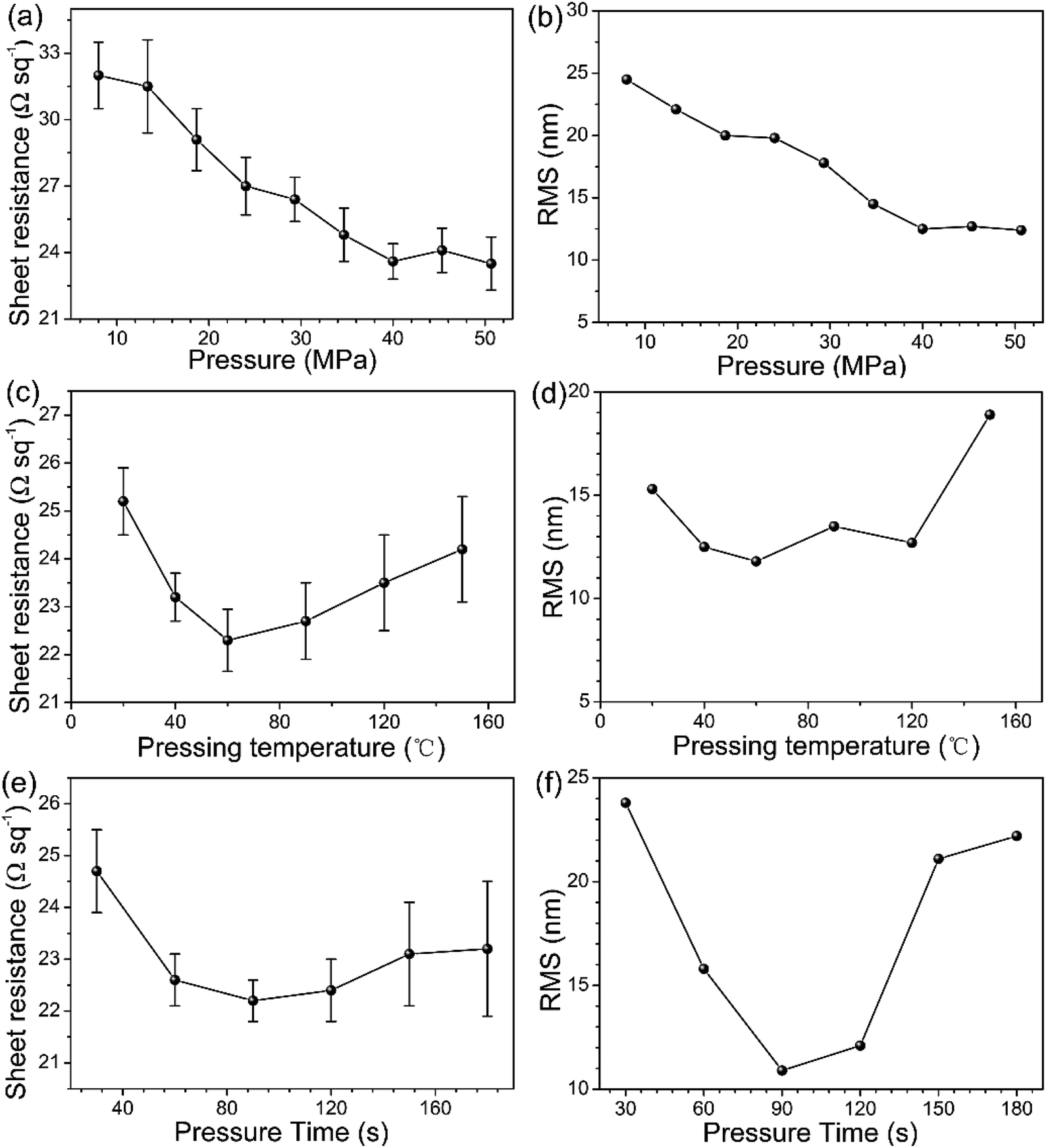 | ||
| Fig. 3 (a) Rsh versus pressure when temperature and time are 40 °C and 120 s and (b) the RMS roughness of the Ag NWs/MEH-PPV composite film versus pressure; (c) Rsh versus pressing temperature when pressure and time are 40 MPa and 120 s and (d) the RMS roughness of the Ag NWs/MEH-PPV composite film changes; (e) Rsh versus pressing time when pressure and temperature are 40 MPa and 60 °C and (f) the RMS roughness of the Ag NWs/MEH-PPV composite film changed. | ||
Similar phenomenon of Rsh variation is observed when the Ag NWs/MEH-PPV electrode is annealed with different temperatures under hot pressing process and the pressure and duration are fixed at 40 MPa and 120 s respectively, as illustrated in Fig. 3c and d, which shows the variation of Rsh for the Ag NWs/MEH-PPV film before and after hot-pressing. When the film annealing temperature is as low as 40 °C, the pristine Rsh is high because of the loose contacts for the Ag NW junctions, so that hot-pressing can bring a huge decrease of 11.5% to Rsh by tightly jointing the Ag NWs. As the annealing temperature directly increase, the contact of nanowires becomes tighter and the effect of pressing is less evident. However, the Rsh has a slight rise when the temperature increases above 60 °C. We speculate the Rsh increase is mainly attributed to poor adhesion between Ag NWs/MEH-PPV electrode and the substrate at high temperature.28 Nevertheless, the final Rsh of films annealed under different temperature are still lower than that of the pristine Rsh, which indicates that the conductivity of films with annealed process under hot-pressing have been largely enhanced.
Fig. 3e and f shows the resistance variations when the pressure duration changes from 30 s to 180 s, while the pressure intensity and temperature are fixed at 40 MPa and 60 °C. The Rsh decreases from 24.7 Ω sq−1 to 22.2 Ω sq−1 after being hot pressed for 90 s, corresponding to a decline about 10.1%, and possess negligible changes when the press time increases from 90 s to 180 s. As the Rsh at 90 s is the lowest value among other duration time, we conclude that 90 s is sufficient to increase the conductivity.
After finishing the preceding optimization studies of Ag NWs/MEH-PPV, AFM images are employed to further characterize the surface morphologies of the resulting Ag NWs samples combined with MEH-PPV color conversion layer, as shown in Fig. 4. In the case of Ag NWs/MEH-PPV color conversion electrode before hot-pressing, the RMS is measured at 21.4 nm (Fig. 4a). In comparison, the RMS of the resulting electrode decreases to 11.8 nm and the surface is smooth. It is also observed that the surface protuberances are decreasing and the film is getting more and more uniform.
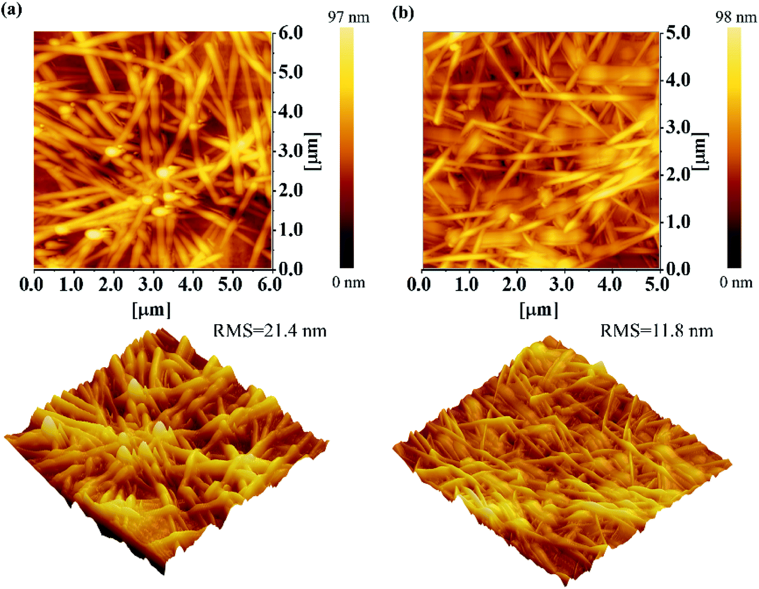 | ||
| Fig. 4 AFM images of optimized Ag NWs/MEH-PPV composite film on PET substrate (a) before and (b) after hot-pressing at 40 MPa and 60 °C for 90 s. | ||
Besides the surface roughness, the flexibility is also a critical parameter for the color conversion electrode. Here, the mechanical flexibility of the composite Ag NWs/MEH-PPV film on PET substrate was evaluated by a bending cycle with a bending radius of 8 mm under convex and concave compression, and the sheet resistance of the sample is measured every 25 bending cycles. R0 and R represent the sheet resistance before and after bending, respectively. An ITO electrode fabricated on PET substrate was also tested as reference. As shown in Fig. S1,† during the bending test, the Rsh of the ITO electrode increases dramatically and the sheet resistance elevates two orders of magnitude after 600 bending cycles. In contrast, the Rsh of the hot-pressed Ag NWs/MEH-PPV color conversion electrode does not alter significantly and keeps almost unchanged during the bending test, which indicates the presence of the tight connections between the Ag NWs.29
3.2 Performance of the flexible blue phosphorescent OLED
To verify the performance of the hot pressed Ag NWs/MEH-PPV with low resistance and surface roughness and evaluate the potential for practical applications, we firstly fabricated flexible blue phosphorescent OLEDs using the Ag NWs as anodes. Fig. 1a schematically displays the structure of the Ag NWs based blue OLEDs on a flexible PET substrate and the electroluminescent performance of the flexible blue OLED is shown in Fig. 5 and Table 1. The blue OLED shows a maximum luminance of 9585.6 cd m−2 and a low turn-on voltage (Von) of 3.8 V, where the Von are extracted at the luminance value of 1 cd m−2 (Fig. 5a). This low Von can be attributed to the high optoelectronic performance of our Ag NWs electrode, the thick junctions on the surface of the hot-pressed Ag NWs film, which are prone to form current pathways between the electrodes. Current efficiency (CE) and external quantum efficiency (EQE) versus luminance are shown in Fig. 5b and c. The maximum CE of the device with Ag NWs anode is 16.3 cd A−1, which is one of the best values among reported Ag NWs anode-based OLEDs in the literature.30,31 Furthermore, the Ag NWs based OLED shows an excellent external quantum efficiency of over 8.5% with the maximum emission peak at 468 nm (Fig. 5d).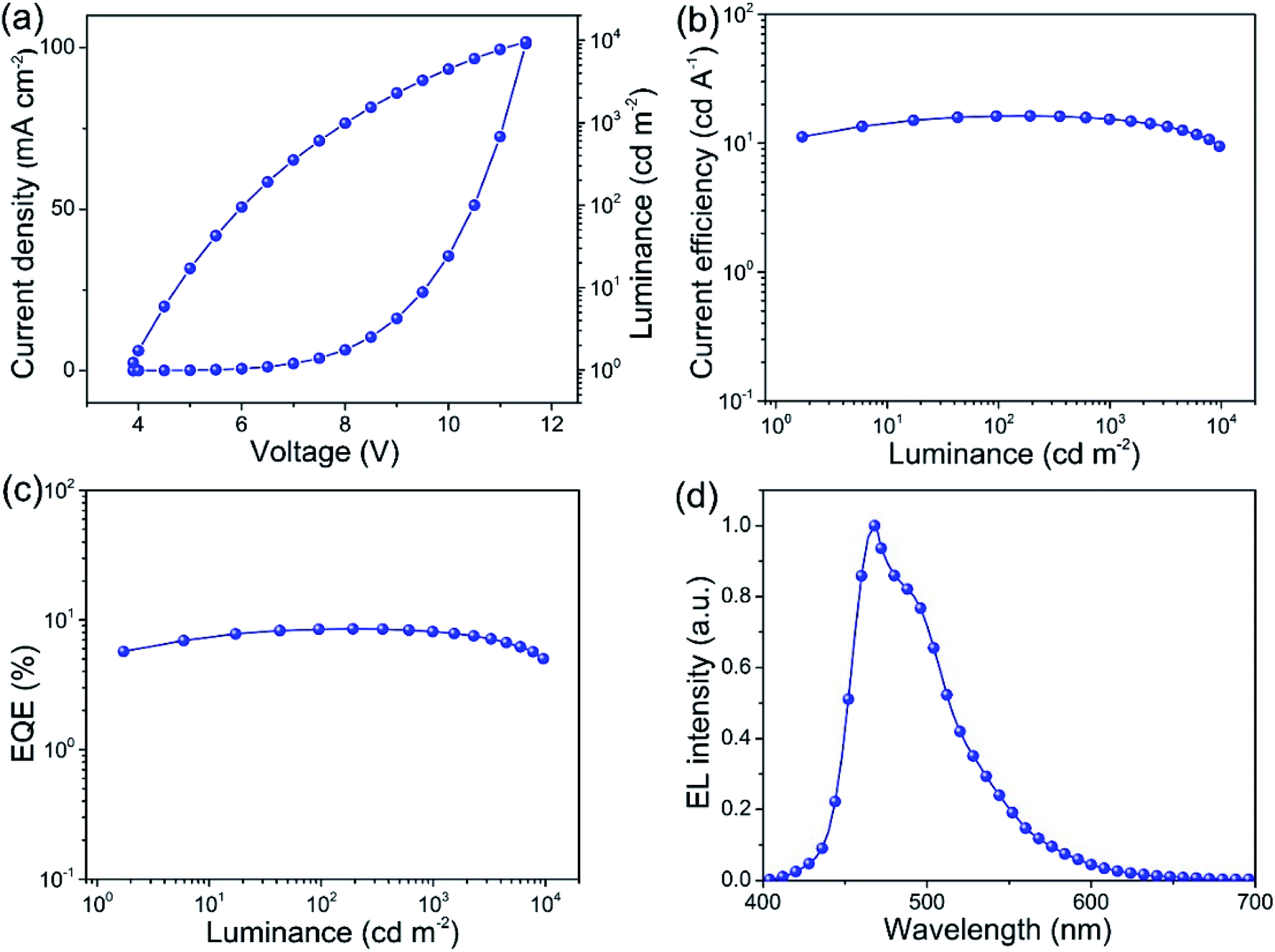 | ||
| Fig. 5 Performance of phosphorescent blue OLEDs. (a) Current density–luminance–voltage (J–V–L) characteristics; (b) current efficiency versus luminance; (c) external quantum efficiency versus luminance and (d) EL emission spectra. | ||
| Devicea | Anode | Vonb [V] | Lc [cd m−2] | CEd [cd A−1] | EQEe [%] | CIEf [x, y] |
|---|---|---|---|---|---|---|
| a Device configuration: anode/TAPC (40 nm)/TCTA (10 nm)/mCP:15%Flrpic (20 nm)/B3PYMPM (40 nm)/Liq (1 nm)/Al (100 nm).b The operating voltage at a brightness of 1 cd m−2.c L, maximum luminance.d CE, maximum current efficiency.e EQE, maximum external quantum efficiency.f CIE coordinates. | ||||||
| B | Ag NWs | 3.8 | 9585.6 | 16.3 | 8.5 | 0.17, 0.39 |
| W1 | Ag NWs/MEH-PPV (100 nm) | 4.2 | 11![[thin space (1/6-em)]](https://www.rsc.org/images/entities/char_2009.gif) 982.0 982.0 |
20.5 | 9.1 | 0.28, 0.30 |
| W2 | Ag NWs/MEH-PPV (160 nm) | 4.3 | 7079.1 | 11.5 | 4.4 | 0.33, 0.37 |
| W3 | Ag NWs/MEH-PPV (200 nm) | 5.5 | 2737.0 | 7.2 | 2.7 | 0.43, 0.41 |
Fig. S2† shows the absorption and photoluminescence spectra of Ag NWs/MEH-PPV color conversion electrode and the EL spectra of Flrpic. The absorption spectrum has a maximum peak at 489 nm. The EL spectrum of emitting layer Flrpic overlaps well with the absorption spectrum of the composite electrode. We expect the efficient down-conversion from blue photons to longer wavelength yellow photons and realize the WOLEDs. The yellow emission from the excited MEH-PPV CCL was centered at 586 nm. The extent of color conversion can be controlled by the amount of the CCL, and the correlated color temperature of flexible WOLEDs is determined by an appropriate balance between the converted yellow emission and the blue EL emission which has not been converted.32 The amount of the MEH-PPV CCL is precisely controlled in order to achieve a high performance white emission. To achieve this goal easily, we prepared a single MEH-PPV CCL and the thickness of CCL was adjusted by controlling the concentration of MEH-PPV layer.
3.3 Performance of the flexible WOLEDs
With the optimization of the fabrication process of blue OLEDs based on Ag NWs electrode, we fabricate flexible WOLEDs as a targeted application and to simplify the WOLEDs fabrication where the Ag NWs-based electrode combined with MEH-PPV acts as a color conversion anode of the WOLEDs with various thickness of MEH-PPV CCL (Device W1: 100 nm, Device W2: 160 nm and Device W3: 200 nm). The WOLEDs device structure is shown in Fig. 1b. Fig. 6 summaries the current density (J) versus voltage, luminance versus voltage, current and external quantum efficiencies versus luminance (L) and the emission spectra of the resulting flexible WOLEDs.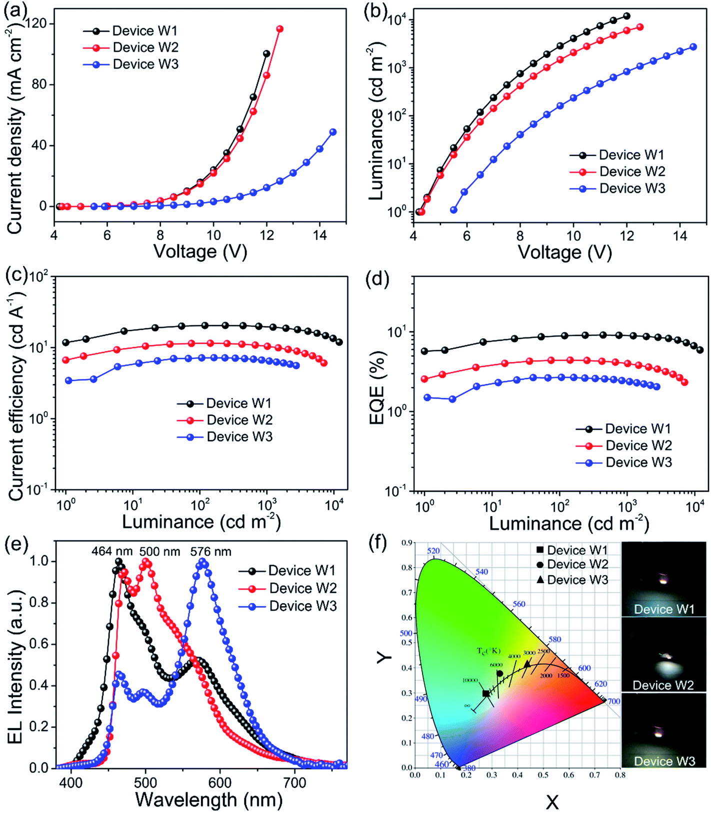 | ||
| Fig. 6 Performance of flexible WOLEDs fabricated on PET substrates based on Ag NWs/MEH-PPV color conversion anode. (a) Current density versus voltage (b) luminance versus voltage (c) CE versus luminance, (d) EQE versus luminance, (e) electroluminescent spectra, (f) the corresponding Commission Internationale de L'Eclairage (CIE) coordinates. (Inset: photographs of the flexible WOLEDs.) | ||
The Ag NWs/MEH-PPV-based WOLEDs (Device W1 and W2) reveal a sharp increase of J values and the low turn-on voltages of 4.2 V and 4.3 V, respectively. The maximum J values of the three WOLEDs with various thickness of MEH-PPV CCL (100, 160 and 200 nm) are 100.5, 116.8, and 49.0 mA cm−2, respectively, with the corresponding maximum L values of 11982.0, 7079.1 and 2723.0 cd m−2 (Fig. 6a and b). Moreover, the peak CEs and EQEs of the three WOLEDs are extracted from the measured J–V–L properties as shown in Fig. 6c and d, to further investigate the effect of different thicknesses of MEH-PPV CCL. The maximum CE of the device W1 with 100 nm MEH-PPV is 20.5 cd A−1 with the corresponding CIE coordinates of (0.28, 0.30), representing one of best performances compared to previously reported CCL based flexible WOLEDs.33 A comparison between our result and other CCL-based WOLEDs is presented in Table S1.† When increasing the thickness of MEH-PPV layers to 160 nm and 200 nm, the maximum CE gradually decreases to 11.5 and 7.2 cd A−1, respectively. This tendency is reconfirmed by the reduction of the maximum EQE in the flexible WOLEDs, where EQEs of 9.1%, 4.4% and 2.7% are observed for the device W1, device W2 and device W3, respectively. The reason of this tendency might be attributed to the decrease of optical transmittance and conductivity, which strongly affects the performance of the WOLEDs. Fig. 6e shows the EL spectra of the three tested WOLEDs with different thicknesses of CCL. Device W1 exhibited cold white emission, indicating insufficient energy transfer from Flrpic to MEH-PPV CCL. Further increasing the thickness of CCL to 160 nm, as predicted, device W2 showed standard white EL spectra, and the CIE coordinate was located at (0.33, 0.37) (Fig. 6f). The emission peak of Device W3 is shown at a wavelength of 576 nm, which is mainly generated from the thicker MEH-PPV CCL in comparison to the main emission peaks (464 nm and 500 nm) from Flrpic for Devices W1 and W2.
To further examine the mechanical stability of the resulting WOLEDs, the device W1 with the highest efficiency was selected as an example to illustrate this point. The temporal change in luminance was monitored under bending deformations in glove box. As shown in Fig. S3,† the device W1 exhibit excellent mechanical flexibility, the initial brightness of 2000 cd m−2 can be maintained over 81% with bending radius of 8 mm under convex and concave compression for 600 cycles. The good stability can be attributed to the good mechanical compliant property of Ag NWs/MEH-PPV, efficient charge carrier injection and high electrical conductivity of the electrodes. Considering that insignificant change in the Rs of the Ag NWs/MEH-PPV electrode was observed at this level of bending radius, the slight decrease in luminance may result from the degradation of the stiffer interfacial layers, such as the vacuum-evaporated Al or interfacial contacts by mechanical deformation. These results suggest that combining WOLEDs with Ag NWs/MEH-PPV color conversion electrode enables the fabrication of extremely flexible and high-performance solid-state lightings.
CIE color coordinates of the device W2 under study is shown in 0.5 V steps of driving voltage in Fig. 7. The X-coordinate of the WOLED varies from 0.3276 (4.5 V) to 0.3261 (at 7.5 V) and 0.3247 (at 10.5 V). This corresponds to a relatively ‘standard white’ color with a correlated color temperature around 5000–6000 K. Differences of the coordinates were negligible due to the intrinsic color stability advantage of the combination of a single-emitter OLED and a color-conversion layer.
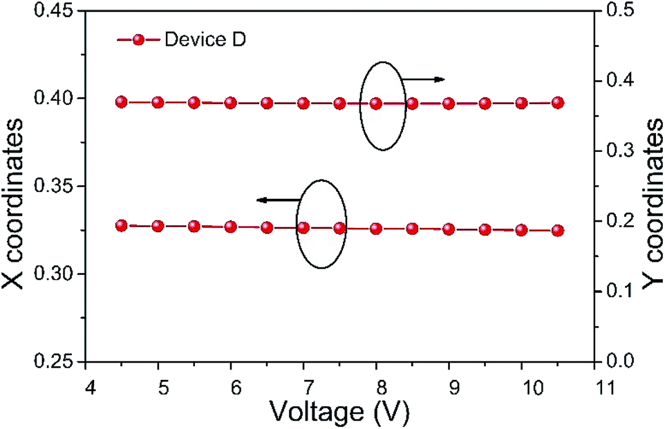 | ||
| Fig. 7 Shifts in CIE 1931 XY-coordinates for the device W2 according to the working voltage changes. | ||
4. Conclusions
In conclusion, a highly flexible, conductive and smooth Ag NWs/MEH-PPV color conversion electrode has been fabricated by a simple hot-pressing method. The solution-processed Ag NWs/MEH-PPV composite film shows a low sheet resistance of 21.8 Ω sq−1 and a low surface roughness. Using the Ag NWs/MEH-PPV composite film as the anode, superior performance of the down-conversion flexible WOLEDs with a maximum current efficiency of 20.5 cd A−1 is achieved with the corresponding CIE coordinates of (0.28, 0.30), which is the first report for the color-conversion electrode based on the Ag NWs for flexible WOLEDs devices. Our work also provides a new avenue of achieving highly efficient flexible optoelectronics for solid-state lighting and display applications.Author's contributions
C. P. and K. L. conceived the new idea and strategy, designed and fabricated the devices, and performed the measurements and analysis with assistance from Z. T., Z. L., H. L., G. C., Y. L., and W. L. B. W. supervised this project and prepared the manuscript with assistance from the other co-authors S. W. and N. Y. All authors have approved the final version of the manuscript.Conflicts of interest
The authors declare no competing financial interests.Acknowledgements
This work is financially supported by the National Key Research and Development Program of China (No. 2016YFB0401303).References
- Y. Miao, K. Wang, B. Zhao, L. Gao, P. Tao, X. Liu, Y. Hao, H. Wang, B. Xu and F. Zhu, Nanophotonics, 2018, 7, 295–304 CAS.
- S. Wang, M. Qiao, Z. Ye, D. Dou, M. Chen, Y. Peng, Y. Shi, X. Yang, L. Cui, J. Li, C. Li, B. Wei and W. Y. Wong, iScience, 2018, 9, 532–541 CrossRef CAS PubMed.
- G. Shi, X. Zhang, M. Wan, S. Wang, H. Lian, R. Xu and W. Zhu, RSC Adv., 2019, 9, 6042–6047 RSC.
- Y. Wu, J. Yang, S. Wang, Z. Ling, H. Zhang and B. Wei, Appl. Sci., 2019, 9, 1415 CrossRef.
- S. Wang, L. Zhao, B. Zhang, J. Ding, Z. Xie, L. Wang and W. Y. Wong, iScience, 2018, 6, 128–137 CrossRef CAS PubMed.
- T. Xu, J.-G. Zhou, M.-K. Fung and H. Meng, Org. Electron., 2018, 63, 369–375 CrossRef CAS.
- Z. Wu and D. Ma, Mater. Sci. Eng., R, 2016, 107, 1–42 CrossRef.
- D. Luo, C. T. Hsieh, Y.-P. Wang, T. C. Chuang, H.-H. Chang and C. H. Chang, RSC Adv., 2018, 8, 30582–30588 RSC.
- C. H. Chang, Y. J. Lo, J. L. Huang, Y. F. Huang, H. Y. Hung, Y. F. Jang and H. H. Chang, Org. Electron., 2014, 15, 1906–1912 CrossRef CAS.
- S. Chen and H.-S. Kwok, Org. Electron., 2011, 12, 677–681 CrossRef CAS.
- L. Tang, S. Cheng, L. Zhang, H. Mi, L. Mou, S. Yang, Z. Huang, X. Shi and X. Jiang, iScience, 2018, 4, 302–311 CrossRef CAS PubMed.
- J. Lewis, S. Grego, B. Chalamala, E. Vick and D. Temple, Appl. Phys. Lett., 2004, 85, 3450–3452 CrossRef CAS.
- C. Guillén and J. Herrero, Thin Solid Films, 2011, 520, 1–17 CrossRef.
- X. Crispin, F. L. E. Jakobsson, A. Crispin, P. C. M. Grim, P. Andersson, A. Volodin, C. V. Haesendonck, M. V. D. Auweraer, W. R. Salaneck and M. Berggren, Chem. Mater., 2006, 18, 4354–4360 CrossRef CAS.
- D. Langley, G. Giusti, C. Mayousse, C. Celle, D. Bellet and J. P. Simonato, Nanotechnology, 2013, 24, 452001 CrossRef PubMed.
- Y. S. Oh, H. Choi, J. Lee, H. Lee, D. Y. Choi, S. U. Lee, K. S. Yun, S. Yoo, T. S. Kim, I. Park and H. J. Sung, Sci. Rep., 2017, 7, 11220 CrossRef PubMed.
- S. Wang, J. Yang, T. Xu, D. Dou, Z. Tang, Z. Gao, M. Chen, K. Guo, J. Yu, J. Plain, R. Bachelot, J. Zhang and B. Wei, Org. Electron., 2019, 64, 146–153 CrossRef CAS.
- S. Coskun, E. Selen Ates and H. E. Unalan, Nanotechnology, 2013, 24, 125202 CrossRef PubMed.
- S. Wang, Y. Zhao, H. Lian, C. Peng, X. Yang, Y. Gao, Y. Peng, W. Lan, O. I. Elmi, D. Stiévenard, B. Wei, F. Zhu and T. Xu, Nanophotonics, 2019, 8, 297–306 CAS.
- S. Kim, H. Lee, S. Na, E. Jung, J. G. Kang, D. Kim, S. M. Cho, H. Chae, H. K. Chung, S. B. Kim, B. W. Lee, K. E. Kim, S. Lee, H. J. Lee, H. Kim and H. J. Lee, Nanotechnology, 2015, 26, 135705 CrossRef PubMed.
- W. Gaynor, S. Hofmann, M. G. Christoforo, C. Sachse, S. Mehra, A. Salleo, M. D. McGehee, M. C. Gather, B. Lussem, L. Muller-Meskamp, P. Peumans and K. Leo, Adv. Mater., 2013, 25, 4006–4013 CrossRef CAS PubMed.
- L. Lian, D. Dong, D. Feng and G. He, Org. Electron., 2017, 49, 9–18 CrossRef CAS.
- Y.-S. Kim, E.-J. Lee, J.-T. Lee, D.-K. Hwang, W.-K. Choi and J.-Y. Kim, RSC Adv., 2016, 6, 64428–64433 RSC.
- K. Zilberberg, F. Gasse, R. Pagui, A. Polywka, A. Behrendt, S. Trost, R. Heiderhoff, P. Görrn and T. Riedl, Adv. Funct. Mater., 2014, 24, 1671–1678 CrossRef CAS.
- G. Haacke, J. Appl. Phys., 1976, 47, 4086–4089 CrossRef CAS.
- E. Jung, C. Kim, M. Kim, H. Chae, J. H. Cho and S. M. Cho, Org. Electron., 2017, 41, 190–197 CrossRef CAS.
- B. Wei, X. Wu, L. Lian, S. Yang, D. Dong, D. Feng and G. He, Org. Electron., 2017, 43, 182–188 CrossRef CAS.
- Y. Jin, D. Deng, Y. Cheng, L. Kong and F. Xiao, Nanoscale, 2014, 6, 4812–4818 RSC.
- M. Hu, J. Gao, Y. Dong, K. Li, G. Shan, S. Yang and R. K. Li, Langmuir, 2012, 28, 7101–7106 CrossRef CAS PubMed.
- W. Zhou, J. Chen, J. Chen, C. Zheng, Z. Gao, B. Mi, H. Zhang and Y. Ma, J. Nanosci. Nanotechnol., 2016, 16, 12609–12616 CrossRef CAS.
- E. Jung, C. Kim, M. Kim, H. Chae, J. H. Cho and S. M. Cho, Org. Electron., 2017, 41, 190–197 CrossRef CAS.
- T. W. Koh, H. Cho, C. Yun and S. Yoo, Org. Electron., 2012, 13, 3145–3153 CrossRef CAS.
- B. S. Kim, M. K. Kim, D. S. Jo, H. Chae and S. M. Cho, ECS J. Solid State Sci. Technol., 2018, 7, 3176–3181 CrossRef.
Footnotes |
| † Electronic supplementary information (ESI) available. See DOI: 10.1039/c9ra04271g |
| ‡ These authors contributed equally. |
| This journal is © The Royal Society of Chemistry 2019 |