
 Open Access Article
 This Open Access Article is licensed under a Creative Commons Attribution-Non Commercial 3.0 Unported Licence
Development of an acetone sensor using nanostructured Co3O4 thin films for exhaled breath analysis†
Parthasarathy
Srinivasan
 a,
Arockia Jayalatha
Kulandaisamy
a,
Ganesh Kumar
Mani
ab,
K. Jayanth
Babu
a,
Kazuyoshi
Tsuchiya
b and
John Bosco Balaguru
Rayappan
*a
a,
Arockia Jayalatha
Kulandaisamy
a,
Ganesh Kumar
Mani
ab,
K. Jayanth
Babu
a,
Kazuyoshi
Tsuchiya
b and
John Bosco Balaguru
Rayappan
*a
aCentre for Nanotechnology & Advanced Biomaterials (CeNTAB), School of Electrical & Electronics Engineering (SEEE), SASTRA Deemed University, Thanjavur 613 401, Tamil Nadu, India. E-mail: rjbosco@ece.sastra.edu; Fax: +91 4362 264120; Tel: +91 4362 264 101 ext. 2255
bMicro/Nano Technology Center, Tokai University, Japan
First published on 24th September 2019
Abstract
In recent times, the development of breath sensors for the detection of Diabetic Keto-Acidosis (DKA) has been gaining prominent importance in the field of health care and advanced diagnostics. Acetone is one of the prominent biomarkers in the exhaled breath of persons affected by DKA. In this background, nanostructured cobalt oxide sensing elements were fabricated using a spray pyrolysis technique at different deposition temperatures (473 to 773 K in steps of 100 K) towards the fabrication of an acetone sensor. The influence of deposition temperature on the various properties of the nanostructured cobalt oxide thin films was investigated. Formation of cubic spinel phase cobalt oxide was confirmed from the structural analysis. The shifting of plane orientation from (3 1 1) to (2 2 0) at 773 K deposition temperature revealed the migration of cobalt atoms to the highly favorable energy positions. Further, the downshifted peak absorption wavelength and upshifted PL profile at higher deposition temperature confirmed the migration of cobalt ions. The sensor fabricated at higher deposition temperature (773 K) showed a sensing response of 235 at room temperature towards 50 ppm of acetone. Also, the fabricated sensor showed a lower detection limit (LOD) of 1 ppm with the response–recovery times of 6 and 4 s, respectively. The LOD reported here is lower than the minimum threshold level (1.71 ppm) signifying the presence of DKA.
1. Introduction
Acetone is the preferred chemical reagent in industries for tissue dehydration, paraffin purification, and plastic dissolution.1 According to the Occupational Safety and Health Administration (OSHA), the human permissible exposure level towards acetone is 1000 ppm as a general industrial standard.2 The National Institute for Occupational Safety and Health (NIOSH) reported the recommended exposure level of acetone as 250 ppm as a time-weighted average.2 Irritation in eyes, skin, and the respiratory system are the general ill-effects caused when the concentration exceeds the permissible exposure limit.2 Acetone is also one of the significant biomarkers indicating the freshness levels of fruits and vegetables.3 From a diagnostic perspective, the presence of trace level acetone (1.8 ppm) in human exhaled breath indicates the presence of Diabetic Ketoacidosis (DKA).4 The concentration of a specific marker present in the exhaled breath is directly related to the metabolic disorders in human beings. Since acetone acts as a fat metabolic nature, the concentration dependence on the exhaled breath is correlated to the fat loss.5 If the patient's exhaled breath contains more than 1.71 ppm of acetone, it indicates the presence of type-2 diabetic mellitus.5 On the other hand, the threshold level of exhaled acetone indicating type-1 diabetes is 2.19 ppm.6DKA is one of the lethal diseases among the different age groups having type-1 diabetes mellitus.7 It affects the patients, especially pregnant women having type-1, type-2, and gestational diabetes. Most common symptoms of DKA in pregnant women are starvation, dehydration, nausea, and cortisol. Onset of DKA is due to the insulin deficiency in the pancreas, which limits the glucose production from the body cells. In this case, instead of getting reacted with glucose, the cells breakdown the fats and results in the production of ketones (acetone) leads to DKA.7
Blood sampling is the conventional clinical technique used for the detection of DKA.7 However, due to its invasive nature, it has not been considered as an efficient diagnostic tool. In this scenario, non-invasive detection of DKA employing exhaled breath analysis has emerged as an effective diagnostic technique.7 Hence, it has been devised to develop an acetone sensor with the following figure of merits such as selective response, fast response & recovery characteristics and LOD in the range of minimum threshold level indicating the onset of DKA.
Recently, ZnO nanostructures decorated with platinum and niobium nanoparticles showed acetone sensing characteristics with the maximum response of 188 and 224 towards 1000 ppm respectively.8 The co-doping strategy has also been reported for the enhanced acetone sensing signatures. Similarly, co-doping of iron and carbon on WO3 nanostructure was reported for the improved acetone sensing performances.9 Another interesting report from Kou et al.,10 depicts the Rh dopant influence on the electrospun SnO2 nanofibers on the acetone sensing characteristics. Rh doped SnO2 nanofibers showed a sensing response of 60.6, which was observed to be 9.6 times higher than that of the undoped SnO2 nanofibers.10 PrFeO3 hollow nanofibers showed noticeable acetone sensing signatures with a maximum response of 6 towards 10 ppm. Mixed potential type sensors based on CeO2 and MMnO3 (M: Sr, Ca, La and Sm) were reported recently, and the composite SrMnO3 exhibited fast response and recovery times of 2 and 6 s respectively towards 20 ppm of acetone.11 But these sensing responses were achieved only at the elevated operating temperatures. Though few room temperature acetone sensors were reported,12–14 the sensing response and transient profiles not significantly pronounced and hence, the present investigation has aimed at the development of room temperature operated, highly selective & sensitive, cost-effective and stable acetone sensor using Co3O4 sensing element with minimum drift against the variations in relative humidity (% RH). In this context, cobalt oxide sensing elements were fabricated using spray pyrolysis technique by varying the deposition temperatures from 473 to 773 K in steps of 100 K.
2. Materials and methods
2.1 Deposition of sensing elements
Cobalt oxide thin films were deposited onto the glass substrates (Blue Star, Mumbai) using automated spray pyrolysis unit (HO-TH-04, HOLMARC, India).15 The precursor solution was prepared by dissolving 0.1 M of cobalt acetate tetrahydrate (Co(CH3CO2)2·4H2O, purity 99.99%, Sigma Aldrich, USA) in 25 mL of deionized water and stirred continuously for 1 h. Meanwhile, the glass substrates were cleaned with deionized water (Millipore, USA) followed by acetone and ultra-sonicated (Supersonic, Mumbai) for 20 min. The precursor solution was loaded into the spray dispenser, and the deposition parameters were optimized. The substrate to spray nozzle distance and solution flow rate were maintained at 15 cm and 1 mL min−1 respectively. The carrier gas (compressed air) with the pressure of 1 bar was maintained throughout the experiment at a solution spray rate of 15 cm min−1.16,17 The solution was sprayed over the glass substrates by varying the deposition temperature from 473 K to 773 K in terms of 100 K respectively. There was no instance of Co3O4 formation was observed below 473 K, and there was no physical stability of Co3O4 thin film was found beyond 773 K (Fig. S1†). Hence, the deposition temperature window was chosen between 473 K to 773 K.2.2 Growth mechanism & reaction scheme
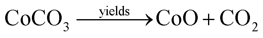
Formation of Co3O4 transforms from the direct decomposition of cobalt precursor into sequential stages starting from the formation of the octahedral phase of Co3+ to Co2+ ions.18 The thermal decomposition reactions of cobalt acetate precursor to cobalt oxide are given in eqn (1)–(3).19 | (1) |
 | (2) |
 | (3) |
As an initial thermal decomposition reaction, the conversion of cobalt acetate to cobalt hydroxide took place by the production of acetic acid. Following the subsequent thermal responses, the formation of CoO occurred, and it gets transformed to stable Co3O4 by the oxidation reaction when it was subjected to annealing at 353 K as given in eqn (4).20
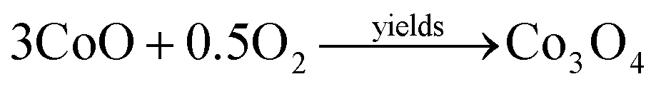 | (4) |
2.3 Characterization and sensor fabrication
Crystal structure of the deposited sensing elements was investigated using X-ray Diffractometer (Bruker, D8 Focus, Germany) with Cu Kα radiation of 1.5418 Å in the 2θ range of 20° to 80°. Morphology of the prepared nanostructures was characterized using Field Emission Scanning Electron Microscope (JEOL, 6701F, Japan). UV-vis spectrophotometer (PerkinElmer, Lambda 25, USA) with the wavelength range of 200 to 800 nm was employed to study the optical properties of the gas sensing elements. Room temperature gas sensing characteristics were studied using customized gas testing chamber integrated with high resistance electrometer (Keithley 6517B, USA).21 Gold Interdigitated Electrode (IDE) pattern was fabricated over the gas sensing element using DC magnetron sputtering. The detailed procedure for IDE fabrication and electrical contacts establishment were reported in our previous work.22 From the fabricated IDE patterns, electrical contacts were established using 25 μm thickness gold wire using wire bonder (TPT wire bonder, HP 05, USA). The concentration of the test analytes was standardized using eqn (5),22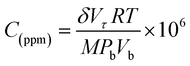 | (5) |
The stable resistance of the sensing element measured at air atmosphere was considered as the baseline resistance (Rair). The change in the resistance of sensor after exposing to the analyte was noted as (Ranalyte). The sensing response was calculated using the eqn (6),
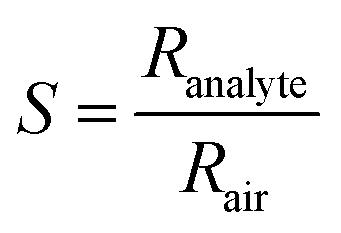 | (6) |
3. Results and discussion
Fig. 1(a) shows the XRD patterns of cobalt oxide thin films deposited at different deposition temperatures. Presence of diffraction planes (220), (311), (222), (400), (511) and (440) in the observed spectra revealed the formation of polycrystalline natured cobalt oxide thin films with cubic spinel phase. The observed XRD pattern is in good agreement with the standard JCPDS card data [78-1970] with lattice parameter a = 8.02 Å. Increasing intensity of (311) planes with deposition temperature, indicated the enhanced crystallinity of the films. However, at 773 K, the preferential plane orientation was shifted from (311) to (220). This could be attributed to the effect of higher deposition temperature, where the atoms get diffused and migrated towards energetically favorable positions by attaining the permanent residency on the surface.23 Lowering of surface free energy could be the reason for the alignment of crystallites towards favourable positions.18,23 Also, the shifting of (311) plane towards a higher angle at higher deposition temperature could be due to the significant grain growth and the influence of surface energy (Fig. 1(b)). The same drift was observed from the morphological analysis, where the grains started to grow with an increase in substrate temperature.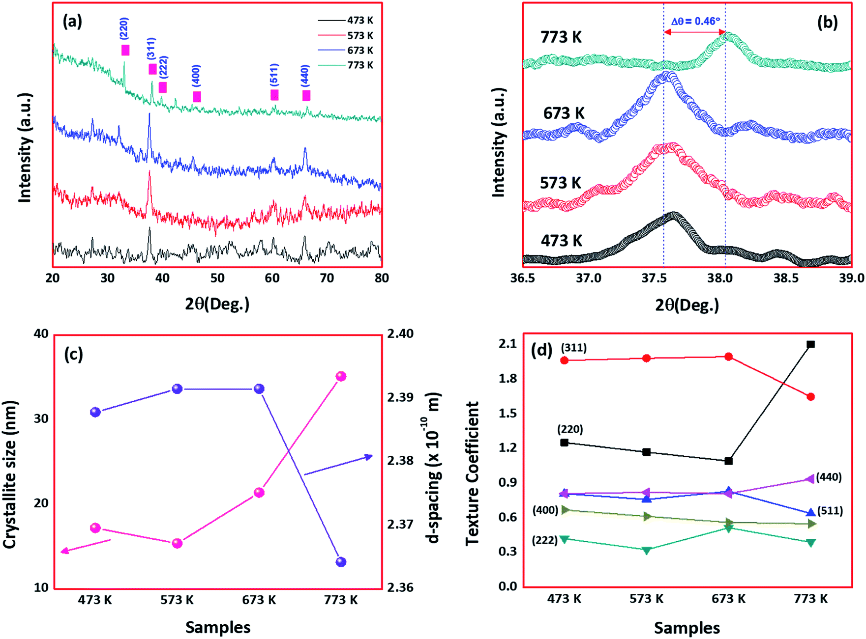 | ||
| Fig. 1 (a) XRD patterns, (b) shift in 2θ of 311 planes, (c) crystallite size & d-spacing, and (d) texture coefficient, of deposited cobalt oxide thin films. | ||
The average crystallite size was calculated using the Debye–Scherrer relation as stated in the eqn (7),
 | (7) |
 | (8) |
Compact surface with smaller spherical nanograins was observed for the film deposited at 473 K, as shown in Fig. 2. Grains get elongated with an increase in deposition temperature. The film deposited at 673 K exhibited clustered grains, which led to the formation of voids on the surface of Co3O4 thin film. Further, at 773 K, grains get thermally agitated and migrated towards lower stable energy position, which might have facilitated the grain clustering and coalescence process.
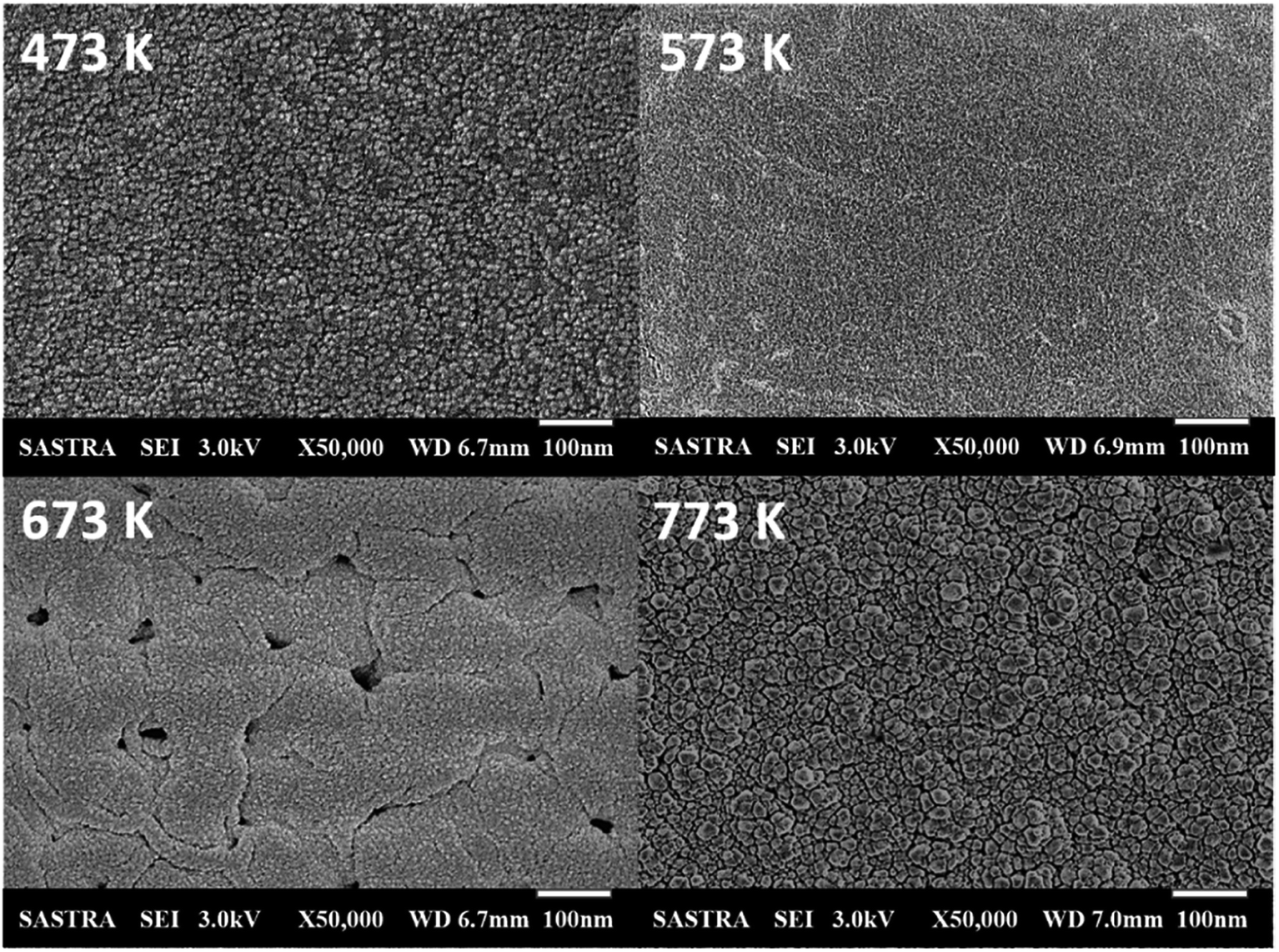 | ||
| Fig. 2 Scanning electron micrographs of cobalt oxide thin films deposited at various deposition temperatures. | ||
The laser spectra analysis of the deposited cobalt oxide thin films is shown in Fig. 3. They revealed the formation of rough surface with an increase in deposition temperature. The film deposited at 673 K showed a maximum enhanced root mean square (RMS) roughness factor in comparison with the other films. The 3D spectra provide strong information about the distribution of particles on the surface. All the deposited thin films showed a maximum distribution of particles around 1 to 2.5 μm. This revealed the impact of deposition temperature in the migration of adatoms on the surface towards favorable energy positions, thereby increasing the distribution of particles and the roughness profile.
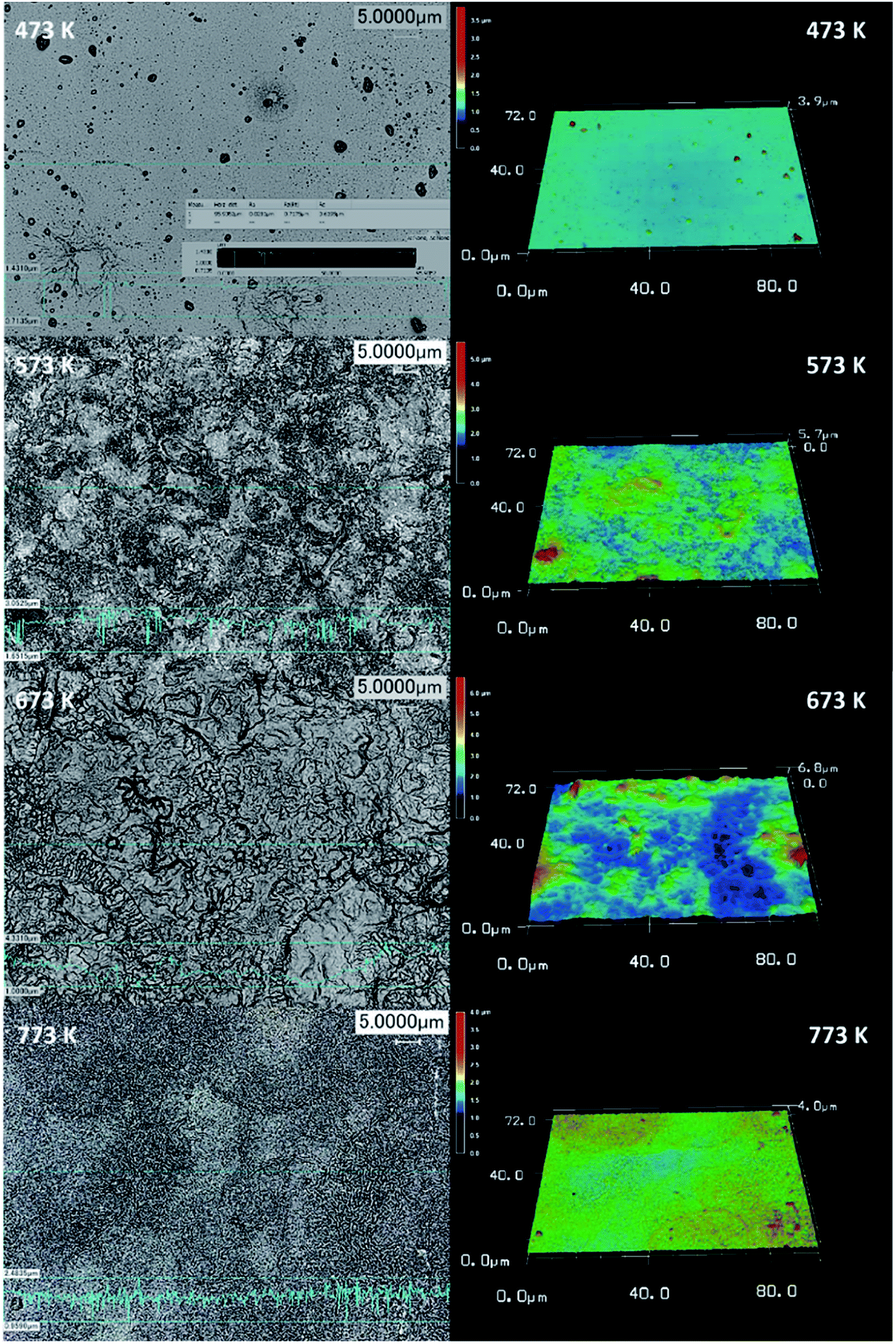 | ||
| Fig. 3 Laser micrographs of cobalt oxide thin films deposited at various deposition temperatures. | ||
XPS spectra of cobalt oxide thin film deposited at 773 K is shown in Fig. 4. Survey spectra shown in Fig. 4(a) confirmed the presence of Co, O, and C elements in cobalt oxide thin film. Existence of Co in 2p, 2s, 3s, and 3p levels was identified from the spectra.
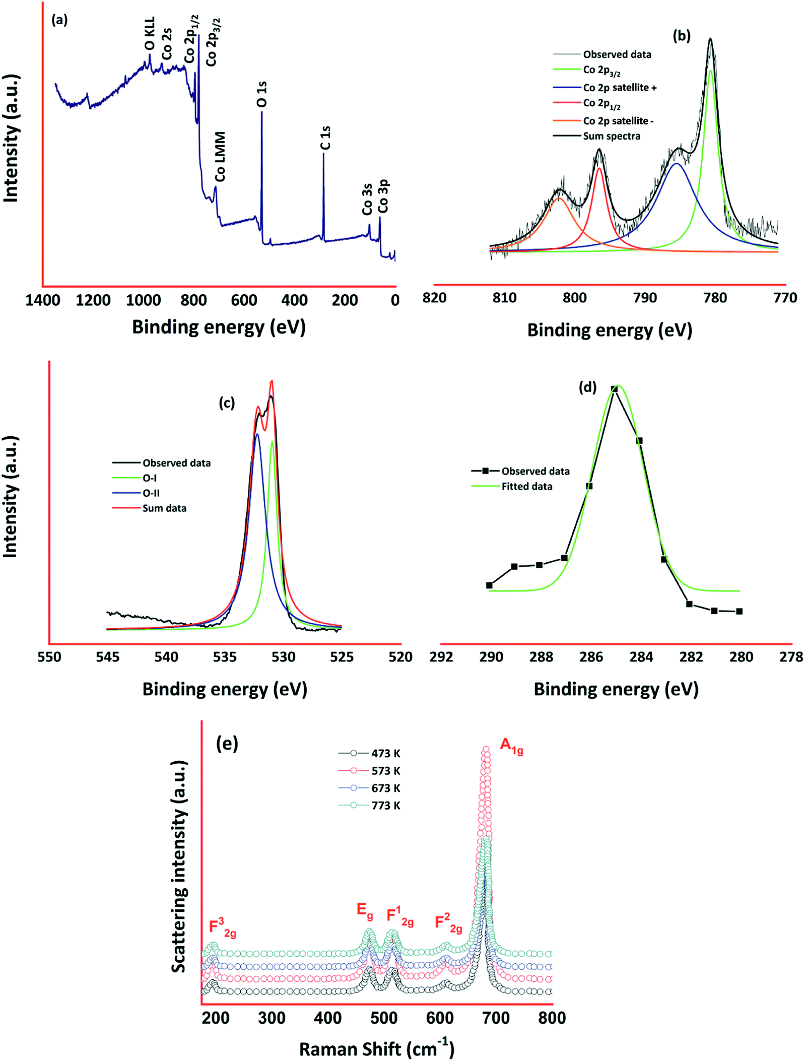 | ||
| Fig. 4 (b) XPS spectra of cobalt oxide thin films prepared at 773 K (a) survey spectra, (b) Co 2p, (c) O 1s, and (d) C 1s spectra, and (e) Raman spectra of cobalt oxide thin films prepared at four different deposition temperatures. | ||
Cobalt 2p core-level spectra comprised of two peaks corresponding to 2p3/2 and 2p1/2 at the binding energies of 780.68 and 796.61 respectively (Fig. 4(b)). The binding energy difference between these two levels was observed to be 15.9 eV and it signifies the splitting of spin–orbit doublet25,26 of Co2+. Deconvoluting the cobalt 2p spectra gives rise to the two small satellite peaks at 785.1, and 801.6 eV corresponding to 2p3/2 and 2p1/2 respectively. Coexistence of tetrahedral Co2+ and octahedral Co3+ was confirmed through the deconvoluted 2p spectra, and it is consistent with the cobalt 2p spectra.27,28 This monovalent and divalent Co species revealed the existence of mixed oxidation states of 2+ and 3+. O 1s spectra (Fig. 4(c)) observed at the binding energy of 530 eV was deconvoluted into two sub-levels at 531.01, and 532.2 eV corresponding to Co–O in Co3O4 and chemisorbed oxygen ions respectively.28,29 Low intense C 1s spectra around 284 eV (Fig. 4(d)) could be comprised of C![[double bond, length as m-dash]](https://www.rsc.org/images/entities/char_e001.gif) C, C–C, C–O, and O–CO.29 Raman spectra of cobalt oxide thin films are shown in Fig. 4(e). Presence of all Raman modes corresponding to the cubic spinel phase of Co3O4 was observed. Peaks centered at 196, 475, 516, 612 and 682 cm−1 correspond to F32g, Eg, F12g, F22g, and A1g modes respectively.30,31 The intensity of these Raman peaks was increased with an increase in deposition temperature. Absence of other Raman modes corresponding to different cobalt oxide phases (CoO and Co2O3) confirmed the existence of cobalt oxide in only Co3O4 phase.32 Due to lower surface energy, the intensity of A1g mode increased drastically for the film deposited at 573 K in comparison with other films. All the peak positions were shifted towards lower wave numbers by 15–25 cm−1, which could be assigned to phonon vector uncertainty in optical phonon confinement effect.33
C, C–C, C–O, and O–CO.29 Raman spectra of cobalt oxide thin films are shown in Fig. 4(e). Presence of all Raman modes corresponding to the cubic spinel phase of Co3O4 was observed. Peaks centered at 196, 475, 516, 612 and 682 cm−1 correspond to F32g, Eg, F12g, F22g, and A1g modes respectively.30,31 The intensity of these Raman peaks was increased with an increase in deposition temperature. Absence of other Raman modes corresponding to different cobalt oxide phases (CoO and Co2O3) confirmed the existence of cobalt oxide in only Co3O4 phase.32 Due to lower surface energy, the intensity of A1g mode increased drastically for the film deposited at 573 K in comparison with other films. All the peak positions were shifted towards lower wave numbers by 15–25 cm−1, which could be assigned to phonon vector uncertainty in optical phonon confinement effect.33
The optical absorbance of the deposited cobalt oxide thin films was observed in the range of 300 to 700 nm (Fig. 5(a)). All the films showed high absorbance in the visible region, and the peak absorption wavelengths were found to be 440, 460, 468 and 420 nm respectively. The films deposited at 573, and 673 K showed larger cut-off wavelength in-turn decreased optical bandgap. The lower peak absorption wavelength of 420 nm for the film deposited at 773 K, indicated the higher energy states of the valence electrons and resulted in the larger optical bandgap.23,34 The optical band gap of the cobalt oxide thin films was estimated using Tauc's relation as expressed in eqn (9),35
| αhν1/n = B(hν − Eg) | (9) |
 | (10) |
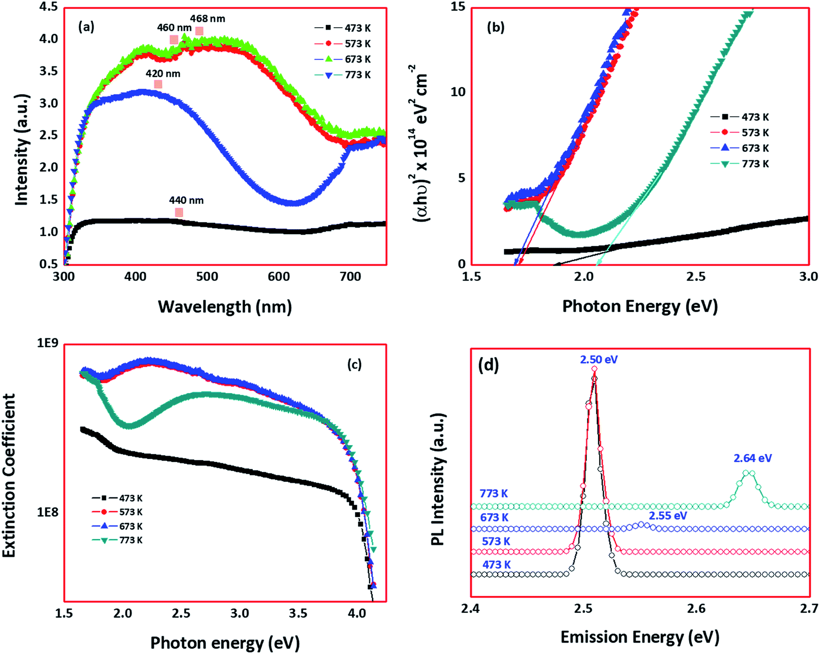 | ||
| Fig. 5 (a) Absorption spectra, (b) optical bandgap, (c) extinction coefficient, and (d) PL spectra, of cobalt oxide thin films deposited at different temperatures. | ||
An increase in the extinction coefficient as a function of deposition temperature was observed (Fig. 5(c)). However, the film deposited at 773 K showed a drastic decrease in the extinction coefficient confirmed the higher energy migration & occupation of Co2+ atoms at elevated temperature.39 Presence of characteristic defect centers in Co3O4 sensing elements was confirmed through room temperature photoluminescence spectra at an excitation wavelength of 440 nm as shown in Fig. 5(d). The sharp peak in the energy region of 2.5 eV (496 nm) could be due to the excitation of charge carriers from the valence band to conduction band defect states.40 In other words, the presence of this defect mode could be assigned to the transition of electrons from OII–CoII (ref. 40) and is in good agreement with the relative intensity of Alg Raman mode. Films deposited at 673 and 773 K showed upshifted peak towards higher energy (2.54 eV and 2.64 eV respectively) indicated the migration of surface Co atoms.41
To extensively investigate the electron transport properties of the cobalt oxide in the grain regime, electrical properties such as carrier concentration, mobility, grain & grain boundary resistances, and activation energy were calculated and listed in Table 1. p-Type behavior of the deposited cobalt oxide thin films was confirmed from the positive values of hall coefficient (RH). Higher carrier concentration and mobility of the film deposited at 773 K could be attributed to the elongated grain profile. Since grain regime decides the transport properties, the boundaries between grains are limited as the grain size increased with deposition temperature. Hence, grain & grain boundary resistances were estimated using AC impedance analysis, as shown in Fig. 6.
| Samples (K) | Carrier concentration × 1010 (cm−3) | Mobility (cm2 V−1 s−1) | Grain resistance (MΩ) | Grain boundary resistance (MΩ) | Activation energy (eV) | C3H6O response |
|---|---|---|---|---|---|---|
| 473 | 3.41 | 36 | 160.3 | 947.6 | 0.457 | 19.4 |
| 573 | 4.19 | 52 | 104.2 | 891.7 | 0.316 | 132 |
| 673 | 4.08 | 93 | 4.4 | 16.1 | 0.252 | 200 |
| 773 | 8.26 | 128 | 6.6 | 12.9 | 0.218 | 235 |
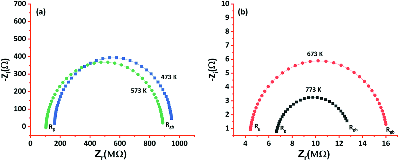 | ||
| Fig. 6 Nyquist impedance plot of cobalt oxide thin films deposited at (a) 473 & 573 K, and (b) 673 & 773 K. | ||
The observed data were fitted to the Randel's equivalent model, and the circuit parameters were calculated. The films deposited at 473 and 573 K showed larger grain and grain boundary resistances in comparison to the other films, and it could be due to the lesser movement of atoms towards favorable energy positions because of deficit thermal energy. On the other hand, a drastic decrease in the grain and grain boundary resistances were observed for the films deposited at higher deposition temperatures (673 and 773 K). Also, it confirmed the limited grain boundaries between the elongated grains and scattering effects.
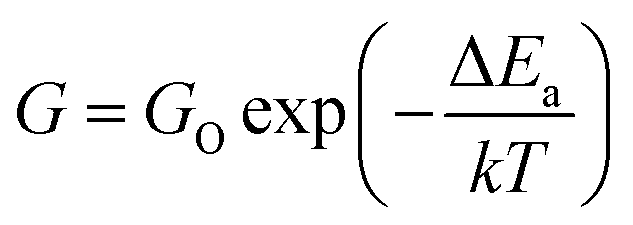
The activation energy of the deposited sensing elements was calculated using the Arrhenius equation (eqn (11)),42,43
 | (11) |
 | ||
| Fig. 7 Arrhenius plots of cobalt oxide thin films deposited at different temperatures. | ||
Selectivity of the sensor is a key parameter in discriminating the specific reactive analyte towards the sensor surface, when the mixture of analytes is presented. In this context, the selectivity of the Co3O4 sensing element were studied in the presence biomarkers (for exhaled breath diseases) such as acetone (C3H6O), ammonia (NH3), ethanol (C2H5OH), xylene (C8H10), toluene (C7H8) and acetaldehyde (C2H4O) and shown in Fig. 8(a). All the sensing elements were highly selective towards C3H6O. The detailed sensing investigations were carried out for the film deposited at 773 K alone, since it showed a maximum sensing response of 235 towards 50 ppm at room temperature.
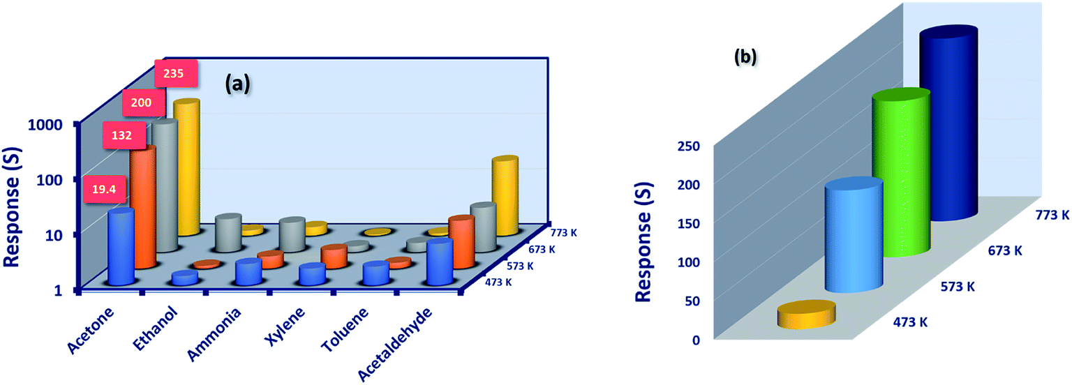 | ||
| Fig. 8 (a) Selectivity of the deposited cobalt oxide sensing elements towards 50 ppm of various analytes, and (b) comparative C3H6O sensing response of the cobalt oxide sensing elements at different deposition temperatures. | ||
The sensing response was found to be increased from 19.5 to 235 for the films deposited at four different substrate temperatures (Fig. 8(b)). This trend could be attributed to the nature of the sensing element and the properties of the test analytes. As far as the properties of gas sensing elements are concerned, the morphology, defect state, crystallinity, and surface roughness decide the selective detection of target analytes.21,42
Enhanced crystallinity with crystal reorientation, shift in the defect states, elongated growth of aggregated nanograins with improved roughness profile of the film deposited at 773 K, could have enhanced the surface with more reactive oxygen sites in-turn resulted in the increased sensing response. On the other hand, the properties of the test analyte such as kinetic diameter, ionization & bond dissociation energy, dipole moments, and HOMO–LUMO energy levels might have influenced the sensing response.42 Since, C3H6O has lower ionization energy, moderate bond dissociation energy and relatively higher kinetic diameter as 9.69 eV, 393 kJ mol−1 and 0.42 nm respectively in comparison with other test analytes, it was highly selective towards the cobalt oxide surface.44 Also, the HOMO–LUMO energy levels of C3H6O might have matched with the bandgap energy of cobalt oxide, which in-turn leads to better sensing response.44
C3H6O interaction with the p-type Co3O4 sensing surface follows sequential reactions at the ambient conditions. The sensing behavior of Co3O4 towards C3H6O is schematically presented in Fig. 9. The room temperature sensing behavior of cobalt oxide depends on the surface adsorption and desorption of C3H6O molecules on the available adsorption sites.44 In the ambient environment, the gaseous oxygen molecules get chemisorbed on the p-type Co3O4 surface by liberating the holes within the Debye length as expressed in eqn (12). As a result, Co3O4 surface gets enriched with majority carriers (holes). As such, the carrier concentration gets increased by reducing the depletion width.44
| O2(gas) ↔ O2(ads)− + h+ | (12) |
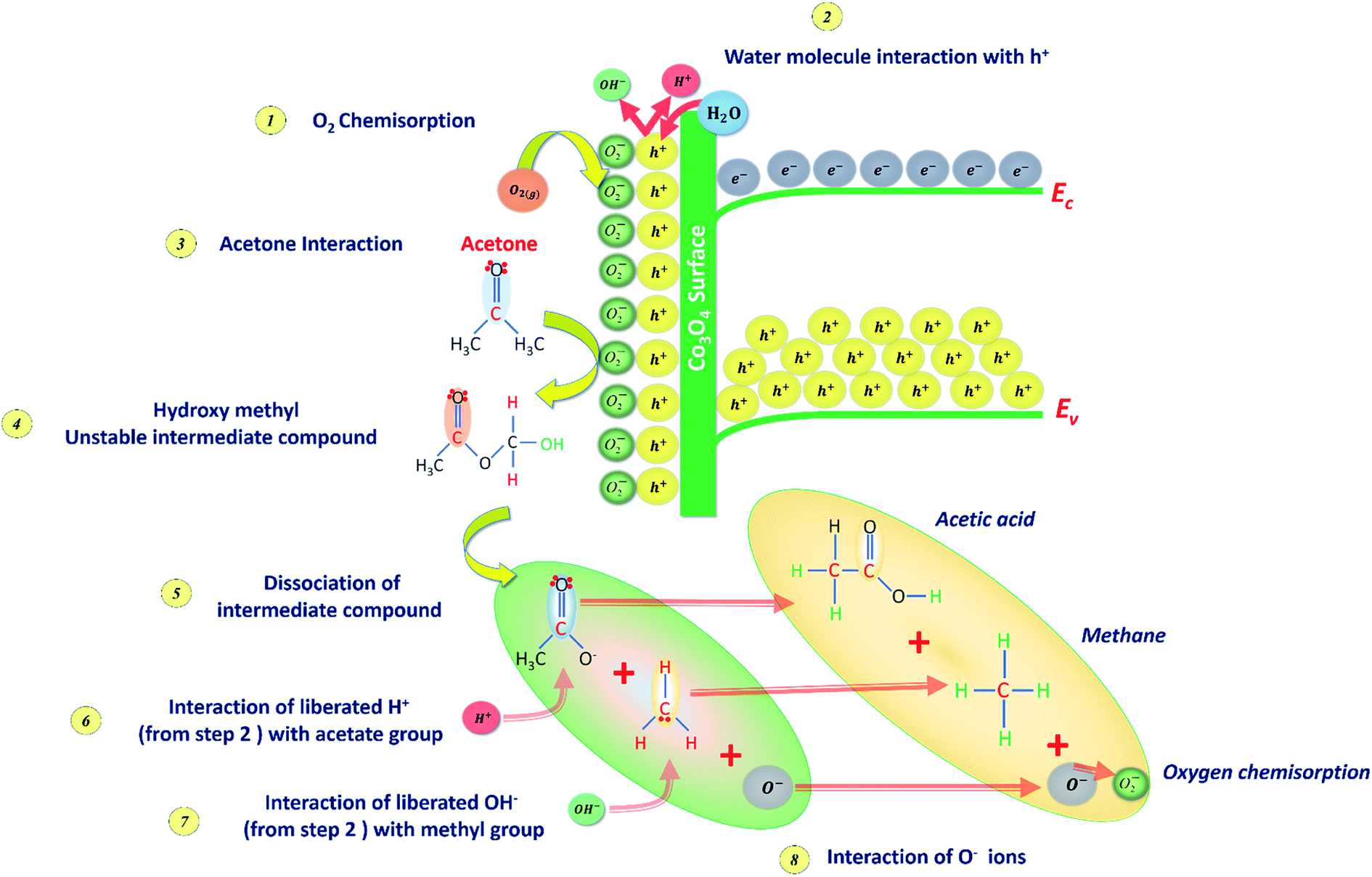 | ||
| Fig. 9 C3H6O sensing mechanism at the cobalt oxide surface represents the sequential interaction stages. | ||
Due to the relative humidity in the ambient, the liberated holes get interacted with the water molecules inside the chamber resulted in the evolution of hydrogen and hydroxyl ions on the surface as depicted in Fig. 9 (step 2) and given in eqn (13),
| H2O + h+ ↔ OH(ads)− + H+ | (13) |
Upon C3H6O interaction with the chemisorbed oxygen species, the formation of an intermediate unstable hydroxymethyl compound CH3–CO2–CH3 gets facilitated as given in eqn (14). As a result of the strong C3H6O–Co3O4 interaction, more oxygen adsorption sites are consumed in-turn decrease the holes concentration.44
 | (14) |
Further, this intermediate unstable compound gets dissociated into methyl group and acetate group. The dissociated acetate group reacts with the hydrogen ion due to its electronegative nature and results in the formation of acetic acid. The remaining OH ions can further dissociate into water and oxygen molecules. Further, chemisorption of these oxygen molecules resulted in the modulation of depletion width. Hence, the sensor resistance gets increased from the initial baseline value and attained stable resistance (Ranalyte). Upon sensor recovery, the interacted C3H6O molecules get desorbed from the surface, and hence the sensor resistance decreased further from the stable resistance and attained baseline air resistance.
C3H6O sensing response towards different concentrations (1–50 ppm) of the film deposited at 773 K is shown in Fig. 10(a). The linear detection range was observed as 1 to 50 ppm (inset of Fig. 10(b)). A more significant change in the sensor resistances was observed with an increase in C3H6O concentration. To confirm the linearity between the C3H6O sensing response and C3H6O concentration, the relation between log(concentration) against log(S − 1) was plotted and shown in Fig. 10(b). The observed plot was fitted to the linear expression y = 2.45728x − 1.8693 with fitting parameter adjacent R2 value as 0.97 indicated the good linearity between the concentration and sensing response.
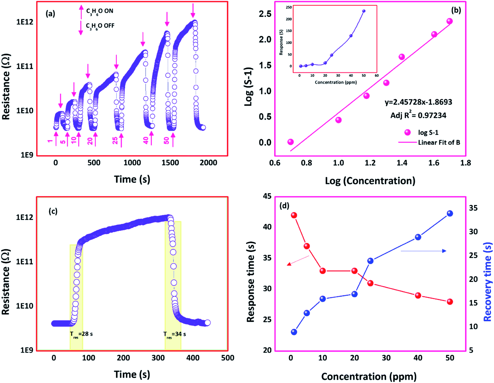 | ||
Fig. 10 (a) Transient response characteristics of the film deposited at 773 K, (b) log![[thin space (1/6-em)]](https://www.rsc.org/images/entities/char_2009.gif) concentration (vs.) log(S − 1) (inset figure is the response trend at different concentration of C3H6O for the film deposited at 773 K), (c) response–recovery times towards 50 ppm, and (d) response–recovery times towards different concentration of C3H6O. concentration (vs.) log(S − 1) (inset figure is the response trend at different concentration of C3H6O for the film deposited at 773 K), (c) response–recovery times towards 50 ppm, and (d) response–recovery times towards different concentration of C3H6O. | ||
Response and recovery times of the film deposited at 773 K were found to be 28 and 34 s respectively towards 50 ppm of C3H6O at room temperature (Fig. 10(c)). At lower concentration of C3H6O, few C3H6O molecules make interaction with the sensor surface, which resulted in the slow response. At higher concentrations of C3H6O, a greater number of C3H6O molecules get interacted, which leads to a faster response and recovery transients (Fig. 10(d)).
To emphasis the salient features of this sensor, its performance has been compared with the literature and presented in Table 2. The LOD of 1 ppm with fast response–recovery, swift transient characteristics, room temperature operation, good repeatability, and long-term stability are the incremental features of the present work.
| S. No | Material & preparation technique | Operating temperature (K) | Response (S) | LOD (ppm) | Ref. |
|---|---|---|---|---|---|
| 1 | Co3O4 nanostructures using spray pyrolysis technique | 303 (RT) | 235 towards 50 ppm | 1 | Present work |
| 2 | ZnO-wire decorated with Pt & Nb using sputtering technique | 673 | 224 towards 1000 ppm for Nb decorated ZnO nanowire | 50 | 45 |
| 3 | SnO2 decorated SiO2 using microemulsion-ultrasonic precipitation | 543 | 2193 towards 300 ppm | 0.5 | 46 |
| 4 | Ytterbium ferrites using sol–gel technique | 503 | 1.72 towards 0.1 ppm | 0.1 | 47 |
| 5 | PrFeO3 hollow nanofibers using electrospinning technique | 453 | 141.3 towards 200 ppm | 10 | 48 |
| 6 | WO3–Cr2O3 using sol–gel technique | 593 | 8.91 towards 20 ppm | 0.5 | 49 |
| 7 | NdFeO3 using sol–gel technique | 393 | 300 towards 50 ppm | 50 | 50 |
| 8 | Cr doped ZnO films using co-sputtering technique | 673 | 90 towards 500 ppm | 15 | 51 |
Since the sensing response is highly reliant on the humid environment, the influence of relative humidity (% RH) on the sensing performance was investigated at various % RH levels. % RH was measured using the Digital Humidity and Temperature (DHT11) sensor integrated to the sensing chamber.22 Different RH levels were maintained by keeping the corresponding saturated solutions inside the sensing chamber.52,53 Change in the sensor baseline resistance at different RH levels is shown in Fig. 11(b). C3H6O sensing responses were decreased by 7.65 and 16.59% at higher humidity levels of 78 and 89% RH, respectively. This could be attributed to the contribution of hydroxyl ions on the sensor surface. The hindrance effect of hydroxyl ions on the chemisorbed oxygen ions limited the C3H6O–CO3O4 interaction which leads to Grotthuss physisorption mechanism. In contrast, sensing response was increased by 3.40% at lower humidity level (32%) due to the hopping charge transport mechanism.52,54–56
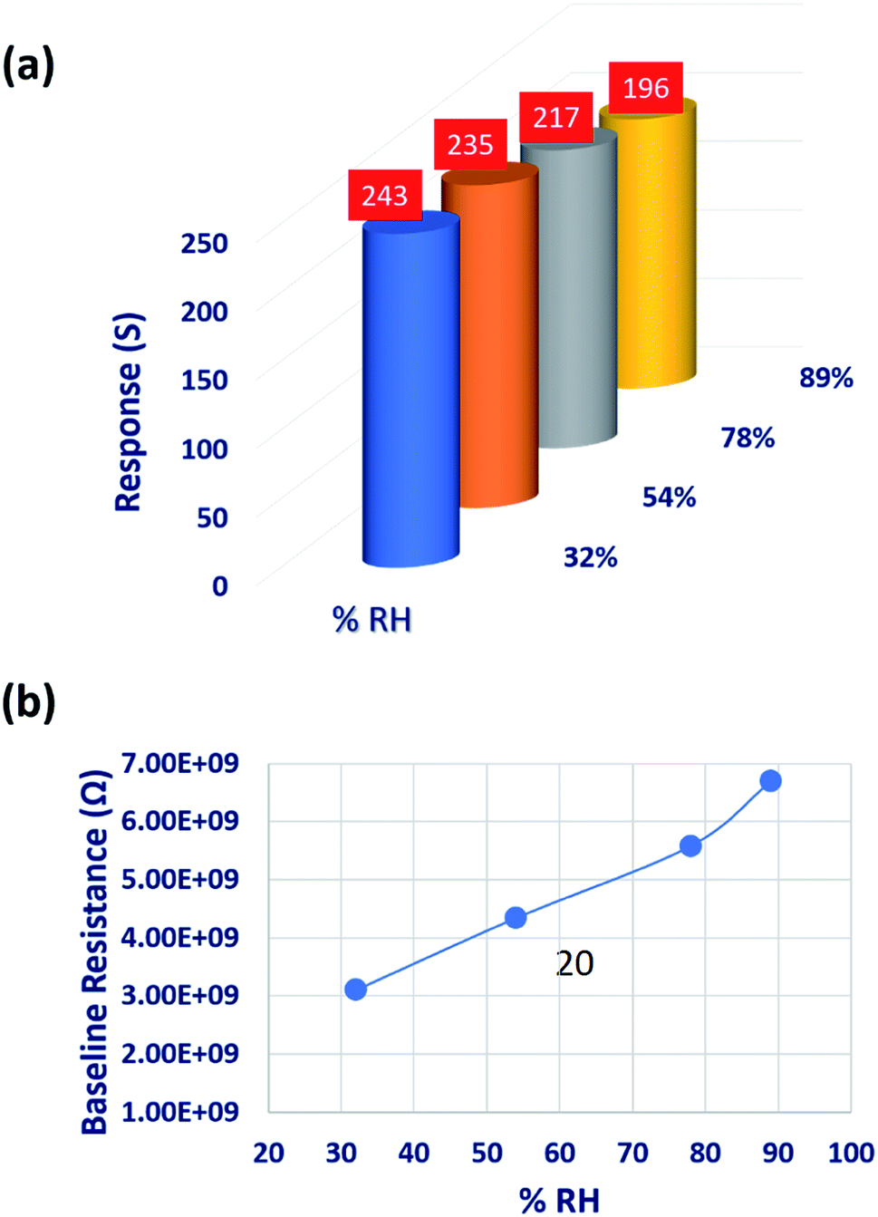 | ||
| Fig. 11 (a) Variation in acetone sensing response, and (b) change in baseline resistance of the sensing element deposited at 773 K, at different RH levels. | ||
Repeatability of the sensor was studied for different cycles, as shown in Fig. 12(a). The sensor showed good repeatability, and the results were reproduced after 4 to 5 response cycles. Stability of the sensor was investigated over 60 days in the interval of 10 days as shown in Fig. 12(b) in which the sensor showed good stability towards 50 ppm of C3H6O even after 60 days. The lowest detection limit of the sensor was observed to be 1 ppm, which is lower than the threshold level of 1.71 and 2.19 ppm. Hence, this sensor can be used to detect the presence of type-2 diabetic mellitus and type-1 diabetes, respectively.5,6
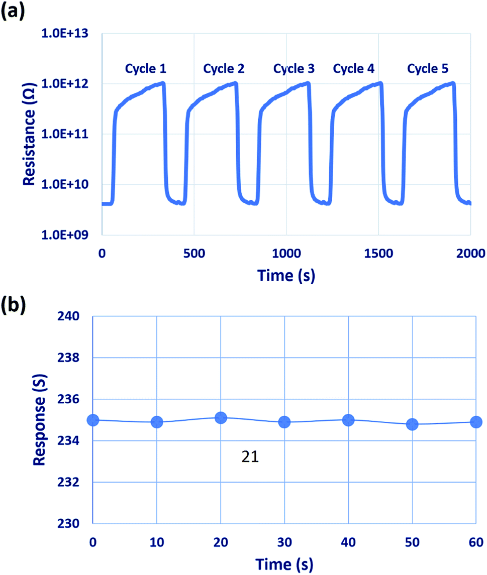 | ||
| Fig. 12 (a) Repeatability of the sensor for five different cycles, and (b) stability of the sensor over 60 days, towards 50 ppm of C3H6O. | ||
Since the developed sensor showed enhanced acetone sensing characteristics at room temperature, the sensing performance of the developed sensor was compared with the sensing performance of commercially purchased Co3O4 nanoparticles (ESI (S1)†). Better sensing response of the Co3O4 thin film than the commercially purchased Co3O4 nanoparticles revealed the significant role of microstructural properties,22,57–62 morphology63–69 and synthesis methods70–73 in deciding the overall sensing performance.
4. Conclusion
Spray deposited nanostructured cobalt oxide thin films were prepared at various deposition temperatures. Microstructural properties of the prepared nanostructures revealed the formation of polycrystalline natured Co3O4 film with cubic spinel phase. The shift in the preferential plane orientation and the formation of aggregated morphology at 773 K deposition temperature revealed the occupancy of Co atoms towards energetically favorable positions. Electrical and optical properties of the prepared nanostructures were also studied as a function of deposition temperature. Room temperature acetone sensing properties of the deposited sensing elements were investigated. The Co3O4 thin film deposited at 773 K showed a maximum sensing response of 235 towards 50 ppm of acetone. Also, the sensor showed the LOD of 1 ppm, which is lower than the threshold level signifying the presence of DKA. Hence, the fabricated sensor can be utilized as a non-invasive diagnosis tool for the detection of trace-level acetone in exhaled breath.Conflicts of interest
There is no conflict of interest to declare.Acknowledgements
Authors wish to express their sincere thanks to the Department of Science & Technology, New Delhi, India, for their financial support SR/FST/ET-II/2018/221 and ECR/2016/001805. One of the authors Mr Parthasarathy Srinivasan, wish to expresses his sincere thanks to the Council of Scientific and Industrial Research (HRDG-09/1095/0016/2016-EMR-I). Authors also thank Nano Mission, DST (SR/NM/PH-16/2007 and SR/NM/PH-04/2015) for their financial support. They also acknowledge SASTRA Deemed University, Thanjavur for extending infrastructure support to carry out this work.References
- J. Kaur, K. Anand, A. Kaur and R. C. Singh, Sens. Actuators, B, 2018, 258, 1022–1035 CrossRef CAS.
- https://www.osha.gov/dts/chemicalsampling/data/CH_216600.html, last visited 18th May 2019.
- M. Ezhilan, N. Nesakumar, K. Jayanth Babu, C. S. Srinandan and J. B. B. Rayappan, Food Res. Int., 2018, 109, 44–51 CrossRef CAS.
- A. J. Kulandaisamy, V. Elavalagan, P. Shankar, G. K. Mani, K. J. Babu and J. B. B. Rayappan, Ceram. Int., 2016, 42, 18289–18295 CrossRef CAS.
- M. Y. Chuang, Y. T. Lin, T. W. Tung, L. Y. Chang, H. W. Zan, H. F. Meng, C. J. Lu and Y. T. Tao, Sens. Actuators, B, 2018, 260, 593–600 CrossRef CAS.
- C. Wang, A. Mbi and M. Shepherd, IEEE Sens. J., 2010, 10, 54–63 Search PubMed.
- M. de Veciana, Semin. Perinatol., 2013, 37, 267–273 CrossRef PubMed.
- E. Wongrat, N. Chanlek, C. Chueaiarrom, W. Thupthimchun, B. Samransuksamer and S. Choopun, Ceram. Int., 2017, 43, S557–S566 CrossRef CAS.
- J. Y. Shen, M. Di Wang, Y. F. Wang, J. Y. Hu, Y. Zhu, Y. X. Zhang, Z. J. Li and H. C. Yao, Sens. Actuators, B, 2018, 256, 27–37 CrossRef CAS.
- X. Kou, N. Xie, F. Chen, T. Wang, L. Guo, C. Wang, Q. Wang, J. Ma, Y. Sun, H. Zhang and G. Lu, Sens. Actuators, B, 2018, 256, 861–869 CrossRef CAS.
- T. Liu, X. Yang, C. Ma, X. Hao, X. Liang, F. Liu, F. Liu, C. Yang, H. Zhu and G. Lu, Solid State Ionics, 2018, 317, 53–59 CrossRef CAS.
- D. Zhang, A. Liu, H. Chang and B. Xia, RSC Adv., 2015, 5, 3016–3022 RSC.
- M. Tabibi, Z. Rafiee and M. H. Sheikhi, in Fundamental Research in Electrical Engineering, ed. S. Montaser Kouhsari, Springer Singapore, Singapore, 2019, pp. 359–367 Search PubMed.
- J. Liang, R. Yang, K. Zhu and M. Hu, J. Mater. Sci.: Mater. Electron., 2018, 29, 3780–3789 CrossRef CAS.
- G. K. Mani and J. B. B. Rayappan, RSC Adv., 2014, 4, 64075–64084 RSC.
- G. K. Mani and J. B. B. Rayappan, J. Alloys Compd., 2014, 582, 414–419 CrossRef CAS.
- G. K. Mani and J. B. B. Rayappan, Superlattices Microstruct., 2013, 67, 82–87 CrossRef.
- P. S. Patil, L. D. Kadam and C. D. Lokhande, Thin Solid Films, 1996, 272, 29–32 CrossRef CAS.
- N. A. M. Barakat, M. S. Khil, F. A. Sheikh and H. Y. Kim, J. Phys. Chem. C, 2008, 112, 12225–12233 CrossRef CAS.
- M. Żyła, G. Smoła, A. Knapik, J. Rysz, M. Sitarz and Z. Grzesik, Corros. Sci., 2016, 112, 536–541 CrossRef.
- P. Shankar and J. B. B. Rayappan, ACS Appl. Mater. Interfaces, 2016, 8, 24924–24932 CrossRef CAS.
- P. Srinivasan and J. B. B. Rayappan, Sens. Actuators, B, 2018, 277, 129–143 CrossRef CAS.
- A. Louardi, A. Rmili, F. Ouachtari, A. Bouaoud, B. Elidrissi and H. Erguig, J. Alloys Compd., 2011, 509, 9183–9189 CrossRef CAS.
- A. S. Enigochitra, P. Perumal, C. Sanjeeviraja, D. Deivamani and M. Boomashri, Superlattices Microstruct., 2016, 90, 313–320 CrossRef CAS.
- H.-J. Lee, S.-Y. Jeong, C. R. Cho and C. H. Park, Appl. Phys. Lett., 2002, 81, 4020 CrossRef CAS.
- Y. Caglar, J. Alloys Compd., 2013, 560, 181–188 CrossRef CAS.
- H. Xia, D. Zhu, Z. Luo, Y. Yu, X. Shi, G. Yuan and J. Xie, Sci. Rep., 2013, 3(1–8), 2978 CrossRef PubMed.
- A. Younis, D. Chu, X. Lin, J. Lee and S. Li, Nanoscale Res. Lett., 2013, 8, 36 CrossRef.
- D. Li, D. Yang, X. Zhu, D. Jing, Y. Xia, Q. Ji, R. Cai, H. Li and Y. Che, J. Mater. Chem. A, 2014, 2, 18761–18766 RSC.
- T. Jakubek, W. Kaspera, P. Legutko, P. Stelmachowski and A. Kotarba, Catal. Commun., 2015, 71, 37–41 CrossRef CAS.
- L. Zhang, X. Zhao, W. Ma, M. Wu, N. Qian and W. Lu, CrystEngComm, 2013, 15, 1389–1396 RSC.
- M. M. Shahid, A. Pandikumar, A. M. Golsheikh, N. M. Huang and H. N. Lim, RSC Adv., 2014, 4, 62793–62801 RSC.
- M. Silambarasan, N. Padmanathan, P. S. Ramesh and D. Geetha, Mater. Res. Express, 2016, 3, 95021 CrossRef.
- A. E. S. M. Hamed, M. A. Siddig and A. A. Elbadawi, International Journal of Scientific Research and Innovative Technology, 2015, 2, 1–5 Search PubMed.
- A. Ashour, M. A. Kaid, N. Z. El-Sayed and A. A. Ibrahim, Appl. Surf. Sci., 2006, 252, 7844–7848 CrossRef CAS.
- S. G. Kandalkar, J. L. Gunjakar and C. D. Lokhande, Appl. Surf. Sci., 2008, 254, 5540–5544 CrossRef CAS.
- A. Bouaoud, A. Rmili, F. Ouachtari, A. Louardi, T. Chtouki, B. Elidrissi and H. Erguig, Mater. Chem. Phys., 2013, 843–847 CrossRef CAS.
- S. Vempati, A. Shetty, P. Dawson, K. Nanda and S. B. Krupanidhi, J. Cryst. Growth, 2012, 343, 7–12 CrossRef CAS.
- Y. F. Yuan, X. H. Xia, J. B. Wu, J. S. Gui, Y. B. Chen and S. Y. Guo, J. Membr. Sci., 2010, 364, 298–303 CrossRef CAS.
- X. De-Sheng, G. Yu, L. Wen-Jing, S. Ming-Su and L. Zai-Wen, Chin. Phys. Lett., 2007, 24, 1756 CrossRef.
- J. C. Toniolo, A. S. Takimi and C. P. Bergmann, Mater. Res. Bull., 2010, 45, 672–676 CrossRef CAS.
- P. Shankar and J. B. B. Rayappan, ACS Appl. Mater. Interfaces, 2017, 9, 38135–38145 CrossRef CAS.
- P. Shankar and J. B. B. Rayappan, J. Mater. Chem. C, 2017, 5, 10869–10880 RSC.
- B. Bhowmik, K. Dutta, A. Hazra and P. Bhattacharyya, Solid-State Electron., 2014, 99, 84–92 CrossRef CAS.
- E. Wongrat, N. Chanlek, C. Chueaiarrom, W. Thupthimchun, B. Samransuksamer and S. Choopun, Ceram. Int., 2017, 43, S557–S566 CrossRef CAS.
- M. Asgari, F. H. Saboor, Y. Mortazavi and A. A. Khodadadi, Mater. Sci. Semicond. Process., 2017, 68, 87–96 CrossRef CAS.
- P. Zhang, H. Qin, W. Lv, H. Zhang and J. Hu, Sens. Actuators, B, 2017, 246, 9–19 CrossRef CAS.
- L. Ma, S. Y. Ma, X. F. Shen, T. T. Wang, X. H. Jiang, Q. Chen, Z. Qiang, H. M. Yang and H. Chen, Sens. Actuators, B, 2018, 255, 2546–2554 CrossRef CAS.
- P. Gao, H. Ji, Y. Zhou and X. Li, Thin Solid Films, 2012, 520, 3100–3106 CrossRef CAS.
- Z. Wu, R. Zhang, M. Zhao, S. Fang, Z. Han, J. Hu and K. Wang, Int. J. Miner., Metall. Mater., 2012, 19, 141–145 CrossRef CAS.
- N. H. Al-Hardan, M. J. Abdullah and A. A. Aziz, Appl. Surf. Sci., 2013, 270, 480–485 CrossRef CAS.
- G. K. Mani and J. B. B. Rayappan, Sens. Actuators, B, 2014, 198, 125–133 CrossRef CAS.
- G. K. Mani and J. B. B. Rayappan, Mater. Sci. Eng., B, 2015, 191, 41–50 CrossRef CAS.
- N. Barsan, M. Schweizer-Berberich and W. Göpel, Fresenius' J. Anal. Chem., 1999, 365, 287–304 CrossRef CAS.
- N. Barsan and U. Weimar, J. Electroceram., 2001, 7, 143–167 CrossRef CAS.
- W. M. Sears, Sens. Actuators, B, 2000, 67, 161–172 CrossRef CAS.
- V. E. Bochenkov and G. B. Sergeev, Adv. Colloid Interface Sci., 2005, 116, 245–254 CrossRef CAS.
- M. M. Arafat, B. Dinan, S. A. Akbar and A. S. M. A. Haseeb, Sensors, 2012, 12, 7207–7258 CrossRef CAS PubMed.
- R. Boppella, P. Manjula, S. Arunkumar and S. V. Manorama, Chem. Sens., 2014, 4, 1–22 Search PubMed.
- S. Majumdar, Ceram. Int., 2015, 41, 14350–14358 CrossRef CAS.
- F. Fang, J. Kennedy, J. Futter, T. Hopf, A. Markwitz, E. Manikandan and G. Henshaw, Nanotechnology, 2011, 22, 335702 CrossRef CAS.
- G. R. Li, T. Hu, G. L. Pan, T. Y. Yan, X. P. Gao and H. Y. Zhu, J. Phys. Chem. C, 2008, 11859–11864 CrossRef CAS.
- K. S. Kim and Y. J. Park, Nanoscale Res. Lett., 2012, 7, 47 CrossRef.
- X. C. Song, X. Wang, Y. F. Zheng, R. Ma and H. Y. Yin, J. Nanopart. Res., 2011, 13, 1319–1324 CrossRef CAS.
- S. G. Victoria, a. M. Ezhil Raj and C. Ravidhas, Mater. Chem. Phys., 2015, 162, 852–859 CrossRef CAS.
- W. Shi and N. Chopra, J. Nanopart. Res., 2011, 13, 851–868 CrossRef CAS.
- J. Y. Lao, J. G. Wen and Z. F. Ren, Nano Lett., 2002, 2, 1287–1291 CrossRef CAS.
- D. Sporn, P. Löbmann, U. Guntow and W. Glaubitt, in Chemical Physics of Thin Film Deposition Processes for Micro- and Nano-Technologies, ed. Y. Pauleau, NAII, Springer, Dordrecht, 2002, vol. 55, pp. 69–89 Search PubMed.
- M. Stan, A. Popa, D. Toloman, T.-D. Silipas and D. C. Vodnar, Acta Metall. Sin. (Engl. Lett.), 2016, 29, 228–236 CrossRef CAS.
- a. Gurlo and M. Ivanovskaya, Sens. Actuators, B, 1997, 44, 327–333 CrossRef.
- S. Kannan, L. Rieth and F. Solzbacher, Sens. Actuators, B, 2010, 149, 8–19 CrossRef CAS.
- X. D. Gao, X. M. Li and W. D. Yu, Appl. Surf. Sci., 2004, 229, 275–281 CrossRef CAS.
- P. V. R. Ramesh, B. K. Ramamurthi and J. V. E. Elangovan, J. Mater. Sci.: Mater. Electron., 2015, 4152–4164 Search PubMed.
Footnote |
| † Electronic supplementary information (ESI) available. See DOI: 10.1039/c9ra04230j |
| This journal is © The Royal Society of Chemistry 2019 |