
 Open Access Article
 This Open Access Article is licensed under a Creative Commons Attribution-Non Commercial 3.0 Unported Licence
Effects of interfaces and current spreading on the thermal transport of micro-LEDs for kA-per-square-cm current injection levels
Chengcheng Lia,
Zhizhong Chen *a,
Fei Jiaoab,
Jinglin Zhana,
Yifan Chena,
Yiyong Chena,
Jingxin Niea,
Tongyang Zhaoa,
Xiangning Kanga,
Shiwei Fengd,
Guoyi Zhangac and
Bo Shena
*a,
Fei Jiaoab,
Jinglin Zhana,
Yifan Chena,
Yiyong Chena,
Jingxin Niea,
Tongyang Zhaoa,
Xiangning Kanga,
Shiwei Fengd,
Guoyi Zhangac and
Bo Shena
aState Key Laboratory for Artificial Microstructure and Mesoscopic Physics, School of Physics, Peking University, Beijing 100871, China. E-mail: zzchen@pku.edu.cn; Tel: +86 13167388462
bState Key Laboratory of Nuclear Physics and Technology, School of Physics, Peking University, Beijing 100871, China
cDongguan Institute of Optoelectronics, Peking University, Dongguan, 523808, Guangdong, China
dSchool of Electronic Information and Control Engineering, Beijing University of Technology, Beijing 100124, China
First published on 5th August 2019
Abstract
The three-dimensional thermal characteristics of micro-light-emitting diodes (μLEDs) on GaN and sapphire substrates were studied with forward-voltage methods, thermal transient measurements, and infrared thermal imaging. The μLEDs on the GaN substrate showed an approximately 10 °C lower junction temperature and smaller amplitude of the K factors than those on the sapphire substrate under the current injection level of 4 kA cm−2. The thermal transient measurement showed that the spreading thermal resistances of the mesa, the GaN epilayer, and the interface of the GaN/substrate were reduced significantly for μLEDs on the GaN substrate because of the high-quality GaN crystal and the homogeneous interfaces. The infrared thermal images showed lower total average junction temperatures and more uniform temperature distributions for the μLEDs on the GaN substrate, which were also simulated with APSYS software. The thermal transport mechanisms are discussed for the lateral and vertical directions in the μLEDs.
Introduction
Micro-light-emitting diodes can operate well at a high injection level of kA cm−2.1–4 The local power density will approach tens of kW cm−2. Most electric power is transferred to the thermal power because of the efficiency droop phenomenon and the increased bulk and contact resistances for small-sized LEDs. There are some reports on the thermal management of μLEDs.4–6 For 40 μm individual LED pixels, the junction temperature (Tj) is about 100 °C at a current density of 4.5 kA cm−2 using the spectral shift method.4 The smaller size μLEDs show lower Tj at same current density. As to the interconnected μLEDs, the thermal resistances also reduce for smaller size LEDs even at the same power density.5 However, the huge power density leads to hot-spots and device failures.7 The Tj distribution in the devices cannot be detected by the spectral shift method.4,5 The thermal dissipation problem is shielded by conventional Tj measurement for μLEDs. Actually, the bulk and spreading thermal resistance of small-size devices becomes higher than that of the broad ones (300 μm × 300 μm).6,8 It is reasonable to assume that the small thermal cross-section makes the dissipation difficult. The lower Tj for smaller sized LEDs is caused by the lower power, uniform current spreading and a sufficient area for thermal dissipation under the same injection level.4,5 There is little possibility of the higher ratio of the sidewall surface area over the active volume when the diameter is larger than 20 μm.9 The spreading thermal resistance will increase further with the increase of the injection level.10 When the proximate μLEDs work together, such as the pixels in the high brightness micro-display,11,12 the complexity of the lighting and the visible light communication (VLC),1 the thermal transport will become more difficult, since the heating μLED will be surrounded by other heavily heating neighbors. In these cases, the design of current spreading, pixel size and geometry may be not effective to obtain the low junction temperature. LEDs on a GaN freestanding substrate can also sustain high injection current densities.13–15 Some researchers report on fabrication of μLED on GaN substrate, while the thermal transport in these devices is not discussed.13Driven by the electric field, electrons gains energy and interact with each other to approach a certain electron temperature. During the relaxation of the hot electrons, the phonons are emitted. Energy then flows from the GaN lattice phonons to the phonons in the sapphire substrate.16 Phonon generation and transport determines the thermal performance of the GaN-based devices. Many imperfections in the solid influence the phonon scattering or diffusion, including threading dislocations, alloy disorders, thermal interfaces, grain boundaries, point defects, and so on.7,16–24 The thermal conductivity (TC) of GaN will decrease to 90 W (m K)−1 or lower when the threading dislocation density (TDD) is above 1010 cm−2.17,18 For similar TDD in a 100 nm-thick AlN epilayer, the TC is suppressed above 100 times compared to that in the bulk AlN.19 If the phonon transport direction is vertical to the TD line, the thermal dissipation becomes more difficult.25 However, the numerous interfaces in LEDs as well as a GaN/sapphire interface provide a lot of possibilities for phonon scattering.16,19–22,24 In some nano systems, phonon transports across interfaces can dictate the overall thermal resistance.7 Some interface structures, such as GaN–diamond interface, GaN/SiC nano-pillar and nano-patterned substrates are applied to enhance the transport of phonons at the interface.20,26,27 Thermal engineering of the materials and their interfaces should also be an important issue for μLEDs under high injection levels.
Many techniques have been developed to characterize the thermal properties of multilayer materials.6,7,10,19–21,24,27–32 Micro-Raman spectroscopy provides a temporal, spectral and spatial resolution for thermal measurement.27 The micron-class spatial resolution cannot satisfy the specific structure of an LED. The absorption for the excitation and Raman scattering of light in different layers should cause large measurement errors.27 For infrared (IR) imaging technology, the IR light emission from the surface of the devices could be measured to assess the lateral temperature distribution.32,33 The temperature resolution can reach to 20 mK, which is much more accurate than 5 K for Raman measurement. Another optical method, named time domain thermal reflectance (TDTR), is usually used to measure the thermal resistance of the materials and their interfaces.7,20,21,24,27 However, the pump and probe instrument and the spectra analysis are complicated for use by unskilled researchers.7 The electrical methods are also popularly used.6,10,19,29–31,34,35 The forward voltage (Vf) is sensitive to the junction temperature.34,35 After the temperature coefficient K is measured, the junction temperature can be obtained in real time according to the voltage. However, the junction temperature measured by the forward voltage method is an average of the temperatures of the whole devices in the vertical and lateral directions. The three-omega method was used to measure the layer-by-layer thermal conductivities of the LED structure through electric frequency modification.19 This method needs a specific sample preparation and a complicated analysis based on an analytical heat conduction model. A transient thermal measurement based on the forward voltage method was developed to analyze multilayer LED package structures.6,10,29–31 The instrument of the transient thermal measurement is easy for a technician to operate even on a commercial LED. By analyzing the cumulative structure function and/or the differential structure function, different components of the LED packages can be recognized. However, there are few reports on the structure functions on the multilayer LED chips.
In this research, different sizes of μLEDs were fabricated on the sapphire and GaN substrates. The thermal properties of the μLEDs were measured with the forward voltage method, infrared imaging, and transient thermal measurement. The temperature distributions in the micro-LEDs were also simulated with the APSYS Packages of Crosslight software. The thermal transport in the chips of the μLEDs was discussed under the injection level of kA cm−2.
Experimental
The same structures of InGaN/GaN multiple quantum well (MQW) LEDs were grown on GaN and sapphire substrates by metal organic chemical vapor deposition (MOCVD). The epitaxial structure consisted of 3 μm undoped GaN, 2.5 μm Si-doped n-GaN, nine periods of GaN (9 nm)/InGaN (2.5 nm) MQW layers with its light emission wavelength at about 390 nm, 20 nm Mg-doped AlGaN electron-blocking layer (EBL), and 230 nm Mg-doped p-GaN. The conventional photolithography and inductively coupled plasma (ICP) etching technology were used to obtain micron-sized pillars with diameters of 10–160 μm and depth of 1.1 μm. The other detailed fabrication procedures can be found in our previous work.3,36 The samples were named after their substrates and pillar sizes. For example, “fs-40 μm” and “ref-40 μm” refer to 40 μm LEDs fabricated on the GaN substrate and on the sapphire substrate, respectively. A KOH solution was applied to repair the etching damage on the sidewalls of the μLEDs. Finally, both of the LED wafers on GaN and sapphire substrates were diced to a piece with a 5 mm × 5 mm area and a 280 μm thickness, where the 16 × 16 pixels μLEDs were included. The optical microscope image of part of the chip is shown in Fig. 1a. Then the chip was directly bonded onto the Al based printed circuit board (PCB) using Ag epoxy. For thermal transient measurement, we bonded the chips with the heatsink using thermal grease. Fig. 1b shows the cross-sectional schematic drawing of the packaged μLEDs prepared for thermal transient measurement. All the μLEDs package employed the same configuration of the components including μLED array chip, Ag epoxy, Al based printed circuit board (PCB), thermal grease and Cu heatsink.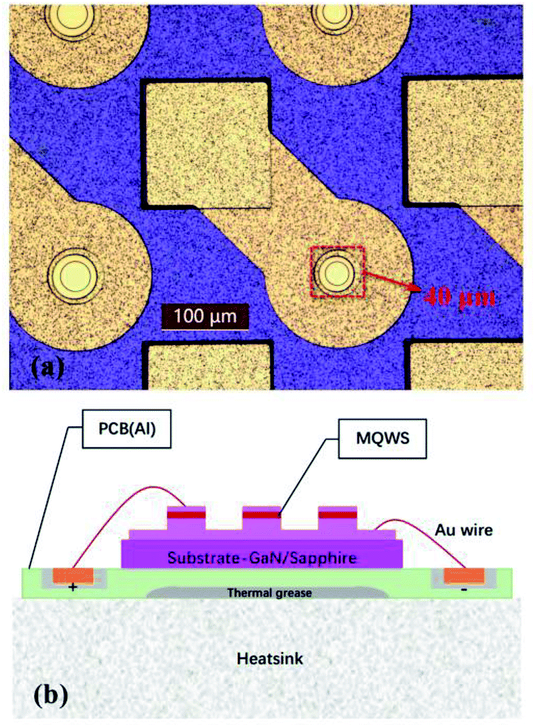 | ||
| Fig. 1 (a) Optical microscope image of the μLEDs. The red frame includes a mesa with a diameter of 40 μm. (b) The schematic of the μLEDs on the GaN/sapphire substrates bonded to the PCB and the heatsink. | ||
The temperature coefficient (K factors) of all the samples were measured using the voltages at a constant sensor current of 10 μA. The sensor current was kept at 10 μA, so the heat generated could be neglected.34,35 The range of the oven temperature was 25 °C to 120 °C. The constant current was provided by a Keithley 2601A system SourceMeter, and the voltage was displayed. The transient thermal measurements were performed with TTE-400 Light Emitting Diodes Thermal Test Equipment by Beijing University of Technology.32,37 The heating time was 300 s and the sampling time was 90 s with an interval of 1 μs. The switch time between the heating and test current was 1 μs. The device was set on a thermoelectric cooler (TEC) using thermal grease and it was operated at a stabilized temperature of 25 °C during the thermal transient measurements. The schematic diagram of the μLEDs on the GaN substrate bonded to PCB and to the heatsink is shown in Fig. 1b. The temperature distribution images of the μLEDs were captured by an FLIR System SC5700 camera with a working wavelength in the 2.1–5.5 μm range and a temperature resolution of 20 mK. The thermal infrared (IR) camera recorded the images with a frequency of 115 Hz (1 ms integration time, 7.6 ms dead time) and a spatial resolution of about 3.0 μm per pixel. The temperature distributions in the micro-LEDs were simulated with an APSYS package of Crosslight software.38 The simulation solved the Poisson equation, the current continuity equations, the photon rate equation, and the scalar wave equation with the current spreading and thermal effect being taken into account.
Results and discussion
Fig. 2 shows the results of the K factors and the junction temperature for different sizes of μLEDs on the GaN and sapphire substrates with various current densities. In Fig. 2a and b, all the samples show the linear behavior of the forward voltage with respect to the oven temperature from 25 °C to 120 °C. Based on the Shockley equation of a diode, the Vf changes linearly with the junction temperature if the ideality factor and the saturation current density stay constant from 25 °C to 120 °C.34 We chose the temperature range because the Tj was below 120 °C when using the following heating power. The 10 μA of the current corresponded to the 0.09–0.80 A cm−2 current density for μLEDs with diameters ranging from 120 μm to 40 μm. In the small injection level, the forward bias was below the turn-on voltage. The Shockley–Read–Hall (SRH) recombination was dominant in the active layer. The corresponding voltages of the μLEDs on the sapphire substrate were 0.3–0.4 V larger than those on GaN substrate were. Better conductivity for the GaN substrate and the strain relaxation in the MQW might reduce the voltage at the same current density.39,40 | ||
| Fig. 2 Forward voltages as functions of temperature at a sensor current of 10 μA for different sizes of μLEDs on the (a) freestanding GaN and (b) sapphire substrates. (c) Temperature coefficients (K factors) of μLEDs with different diameters on the GaN and sapphire substrates. (d) Junction temperature versus current density for the samples of fs-40 μm, ref-40 μm, fs-120 μm, and ref-120 μm. | ||
K factors of μLEDs on different substrates were obtained as negative values according to the data in Fig. 2a and b, as shown in Fig. 2c. For convenience, the K factors mentioned in the following sections represent the absolute values of those negative values. With the size increasing, the K factors increased for these μLEDs. Moreover, the K factors of the μLEDs on the freestanding GaN were lower than those on the sapphire substrate were. The K factors of the μLEDs from 2.32 mV °C−1 to 2.54 mV °C−1 on the sapphire were similar to the broad LEDs on the sapphire substrate elsewhere,34,35 while the values of the μLEDs on the freestanding GaN ranged from 1.92 mV °C−1 to 1.99 mV °C−1. The K factor decreased when the crystal quality was improved by patterned sapphire substrate.32 But it does not change when the sensor current varied from 10 mA to 110 mA.34,35 The TDD was approximately 5 × 106 cm−2 in the LED epilayer on the GaN substrate, which was two orders lower than that on sapphire substrate. It is reasonable to conclude that the smaller K factors on the GaN substrate can be attributed to its high crystal quality. For the K factors that varied with the diameter, the different current density seemed not to be the cause. However, the injection levels were different between ref. 34, 35 and our work. According to the reports of these researchers, the injection levels were approximately 10–100 A cm−2, while ours were approximately 0.09–0.80 A cm−2. For moderate or high injection levels, the dependences of the current–voltage (I–V) curves on the temperature might not have been significant. Moreover, an additional voltage might have appeared when the polarization field increased due to more strain.39 In large size μLEDs, the strain was less relaxed than that in small size ones.36,41 With the temperature increases, the strain in MQW increased due to the thermal mismatch between the GaN and the InGaN. This trend indicates that the smaller K factor on GaN substrate could be partially caused by the strain relaxation in the MQWs.40
According to the K factors, the junction temperatures were calculated for 40 μm and 120 μm LEDs on freestanding GaN and sapphire substrates, as shown in Fig. 2d. The junction temperature increased with the increase of the current density. It is clear that the junction temperature increased rapidly for larger size of μLEDs or for the μLEDs on the sapphire substrate. Specifically, along the horizontal dotted line in Fig. 2d, the corresponding current densities were 9.0 kA cm−2, 6.0 kA cm−2, 1.2 kA cm−2, and 1.0 kA cm−2 when the junction temperature reached 70 °C for the samples of fs-40 μm, ref-40 μm, fs-120 μm, and ref-120 μm. It is clear that smaller size μLEDs have lower junction temperature when operated under same current density. Considering the mesa area, the electric powers of the 120 μm μLEDs were much higher than those of the 40 μm μLEDs when operated under same current injection density. The thermal resistance was higher for the small size μLEDs, while their junction temperature was much lower than that of the large size μLEDs. The uniform current density and the strain relaxation improved the luminous efficiency, which cut down the thermal loss in the small size μLEDs.4,36,41 With regard to the effect of the substrate, both the thermal resistance and the junction temperature for the μLEDs on the GaN substrate were lower than those on sapphire substrate were. This was due to the high conductivity for the low TDD GaN epilayer and the GaN substrate.17,18
The forward voltage method provided the average junction temperatures of the μLEDs. However, this was not enough to understand the thermal transport across the multiple interfaces. To distinguish the effects of the components and their interfaces on the total thermal resistance, thermal transient measurements were carried out for the μLEDs. The structure functions of the μLEDs could be obtained from the cooling curves of the μLEDs. The schematic of the thermal transient measurement setup is shown in Fig. 1b. The heat flow in the figure was from the pn junction to the bottom heatsink. Fig. 3 shows the typical cumulative and differential structure functions for 40 μm LEDs, where the Cth and Rth terms represent the thermal capacitance and the spreading thermal resistance, respectively. In Fig. 3a, the step-shaped curves can be observed for 40 μm LEDs on different substrates. The steep segments correspond to the relative high heat capacitance and the low spreading thermal resistance, which are contributed by the components of the LED devices. These components include mesa, GaN epilayer, substrate, PCB, Ag epoxy, and Cu heatsink.29,31 Conversely, the flat segments can be attributed to the thermal interfaces between the components. In Fig. 3b, several peaks can be observed in the differential curves; these peaks represent the component locations at the thermal resistance axis.29,42 Some researchers think that the peaks in the differential curves correspond to the material interface.30 In this work, the peaks in Fig. 3b correspond to the steep segment in Fig. 3a. This means that the peaks cannot be attributed to the interfaces between the components because of their low spreading thermal resistance and high heat capacitance.
 | ||
| Fig. 3 (a) Cumulative structure functions and (b) differential structure functions for the samples of ref-40 μm and fs-40 μm. Both the μLEDs were operated under 4 kA cm−2. | ||
The curves in Fig. 3 are divided into nine parts, as marked by the capital letters A–I for the sample of ref-40 μm. The curve for the fs-40 μm sample is also marked by “A–I”, but the corresponding spreading thermal resistance values that these letters represent are different than those for the ref-40 μm sample shown in Fig. 3. Table 1 lists the spreading thermal resistances of the components and their interfaces, drawn from the structure functions. Segment A refers to the mesa with a 40 μm diameter and a 1.1 μm height. The spreading thermal resistances of 3.43 °C W−1 and 6.08 °C W−1 correspond to the thermal conductivities (TCs) of 200 W (m K)−1 and 113 W (m K)−1 for the fs-40 μm and ref-40 μm samples, respectively. The TC could reach up to 230 W (m K)−1 for a freestanding GaN.18 With the TDD increasing, the TC decreased sharply.17,18 This results indicates that the TDD in the mesa of the fs-40 μm sample was two orders lower than that of the ref-40 μm sample. The alloy disorder and the MQW interfaces could also scatter the phonons and reduce the TC.19 Segment B refers to the 5 μm-thick GaN epilayer around the mesa. If the TCs in the broad GaN epilayers stayed unchanged compared to those in the mesas, the small spreading thermal resistances meant that the thermal cross-sectional area increased about 30 times. The fs-40 μm sample clearly showed lower spreading thermal resistance. Correspondingly, a peak appeared in Segment B in the differential curves, as listed in Table 1. The peak width of the fs-40 μm sample was narrower than that of the ref-40 μm sample. The lower width indicates a higher epilayer crystal quality for the fs-40 μm sample. Segment C refers to the interfaces between the two materials. We attributed this to the interface between the epilayers and the substrates. If the effective contact area was about 30 times, the thermal interface conductivity for the ref-40 μm sample was about 5 MW (m K)−1. This was of the same order as the AlN/SiC interface.15 This was reasonable for the defective GaN crystal with a large amount of misfit dislocation, nitrogen vacancies, and grain boundaries at the interface. However, for the GaN epilayer on the GaN substrate, the interface spreading thermal resistance of 2.40 °C W−1 seemed larger than the prediction. For this homogenous interface, the interface spreading thermal resistance might come from the regrowth with MOCVD on the hydride vapor epitaxy (HVPE) GaN substrate. A transition layer was required for the MOCVD regrowth, which might not match with both the GaN substrate and the GaN epilayer. Furthermore, the GaN material might show different mechanical properties with different growth techniques, which could affect the acoustic phonon matching.21,22 Moreover, the effective interface area for the fs-40 μm sample would be less than that of the ref-40 μm sample because the vertical thermal transport was rapid due to the lower bulk and the interface spreading thermal resistances for the fs-40 μm sample. The small thermal spreading interface area for the fs-40 μm sample will be evidenced in the following infrared imaging results.
| Segments | Type | Spreading thermal resistance of the segments in the cumulative structure function (°C W−1) | Location of the peaks in the differential structure function (°C W−1) | ||
|---|---|---|---|---|---|
| fs-40 μm | ref-40 μm | fs-40 μm | ref-40 μm | ||
| A | Mesa and MQWS interface | 3.43 | 6.08 | ||
| B | GaN epilayer | 0.54 | 0.87 | 3.6 | 6.25 |
| C | Interface of epilayers and substrates | 2.40 | 4.32 | ||
| D | Substrate | 0.69 | 0.94 | 6.81 | 11.94 |
| E | Substrate and Ag epoxy | 2.93 | 2.93 | 8.43 | 13.65 |
| F | Interface of Ag epoxy and PCB(Al) | 6.40 | 5.24 | ||
| G | PCB(Al) | 2.72 | 5.40 | 17.9 | 22.24 |
| H | Thermal grease interfaces of PCB/thermal grease and thermal grease/heatsink | 6.60 | 9.56 | ||
| I | Heatsink | 0.92 | 1.03 | 26.63 | 36.38 |
Segment D represents the spreading thermal resistance of the GaN or sapphire substrate. The TCs of the sapphire substrate was approximately 45 W (m K)−1. Therefore, the thermal resistance of 0.94 K W−1 for the 280 μm-thick sapphire corresponded to the effective thermal spreading cross-section of approximately 6.6 mm2, which was a quarter of the total area of the chip. This means that the 280 μm thermal path made the thermal spreading cross-section increase about 20 times. The TCs of the freestanding GaN was approximately 230 W (m K)−1. The thermal spreading cross-sectional area for the GaN substrate was approximately 1.8 mm2. This was due to the rapid vertical thermal transport discussed above, which will be evidenced by IR thermal imaging results. The peaks in the differential curves also appeared in this area. Clearly, the sharp peak for the GaN substrate was due to the small spreading thermal resistance compared to the sapphire substrate. Segment E corresponds to a slow increase. A peak appeared in the segment shown in the differential curve. This referred to the Ag epoxy. The spreading thermal resistance of the Ag epoxy was the same for the fs-40 μm and ref-40 μm samples, which means that the Ag epoxy coating procedure was well controlled. There was almost no platform between Segments E and D due to the interface spreading thermal resistance, which could be neglected. Segment F refers to the interface between the Ag epoxy and the Al based PCB. The obvious and large spreading thermal resistances of this interface indicated that the metal and the epoxy had large thermal barriers, which might be due to the difference of the densities of the phonon states. Only the spreading thermal resistance in Segment F for the fs-40 μm sample was larger than that of the ref-40 μm sample. This may be also due to the small thermal spreading conduction area, since the thermal interface conductivity was similar. Segment G refers to the PCB. The TCs of the thermal grease was approximately 1 W (m K)−1. The thermal resistance of the thermal grease could be calculated and the value was 0.8 K W−1. As we see in Fig. 3a and b, the flat segment of Segment H refers to the combination of thermal grease, interfaces of PCB/thermal grease and thermal grease/heatsink. Segment I represent the heatsink, which was similar for both fs-40 μm and ref-40 μm samples. For the Segments of G and H, the spreading thermal resistances were much lower for the fs-40 μm sample than for the ref-40 μm sample. Although the thermal structures in Segments of G and H were similar for both two samples, the thermal resistances and capacitances were quite different. Hence, the temperature and its distribution near the PCB were different for the two kinds of samples. The smaller spreading thermal resistance and the capacitance for high-quality GaN led to a higher temperature and a more uniform temperature distribution in Segment H than those for sapphire substrate.
The structure function analyses provided the information for the partial spreading thermal resistance for the materials and their interfaces. However, the lateral thermal transport for the μLEDs was not clear yet. In order to understand the thermal transport comprehensively, IR thermal imaging was performed on the fs-40 μm and ref-40 μm samples. The samples were operated from 0.2 kA cm−2 to 15 kA cm−2 and the corresponding thermal images were captured when the samples stabilized. A germanium wafer was used as a filter in both the calibration and measure processes to avoid the heating of the detector and the lens. We acquired the final IR data after averaged three images under same current injection density. The measurement uncertainty of IR measurement is described by standard deviations (SD) with the scope of 0.024–0.179 °C in this manuscript. Fig. 4a and b shows the IR thermal images of fs-40 μm and ref-40 μm samples operated at 4 kA cm−2. The temperature scale bars were put on the right side of the thermal images in the same range from 41.90 °C to 54.05 °C for comparison. The dashed lines in both Fig. 4a and b represent the real diameters, which were about 40 μm. It can be clearly seen that the temperature was higher on the mesa than the surrounding parts. The temperature distribution on the mesa was relatively uniform. There was a temperature gradient around the mesa. The average temperatures were 43.25 °C and 53.16 °C on the mesa for the fs-40 μm and ref-40 μm samples, respectively. The temperature differences between the mesa and surroundings were about 1 °C and 12 °C for the fs-40 μm and ref-40 μm samples. It is reasonable from Fig. 3 to prefer the mesas as one individual component of the chip based on the thermal images. It can also be determined that the lateral thermal transport for the ref-40 μm sample was more significant than that for the fs-40 μm sample due to the higher temperature gradient. The temperature of the surroundings was lower than that of the mesa. However, the temperature was still about 20 °C higher than the ambient temperature.
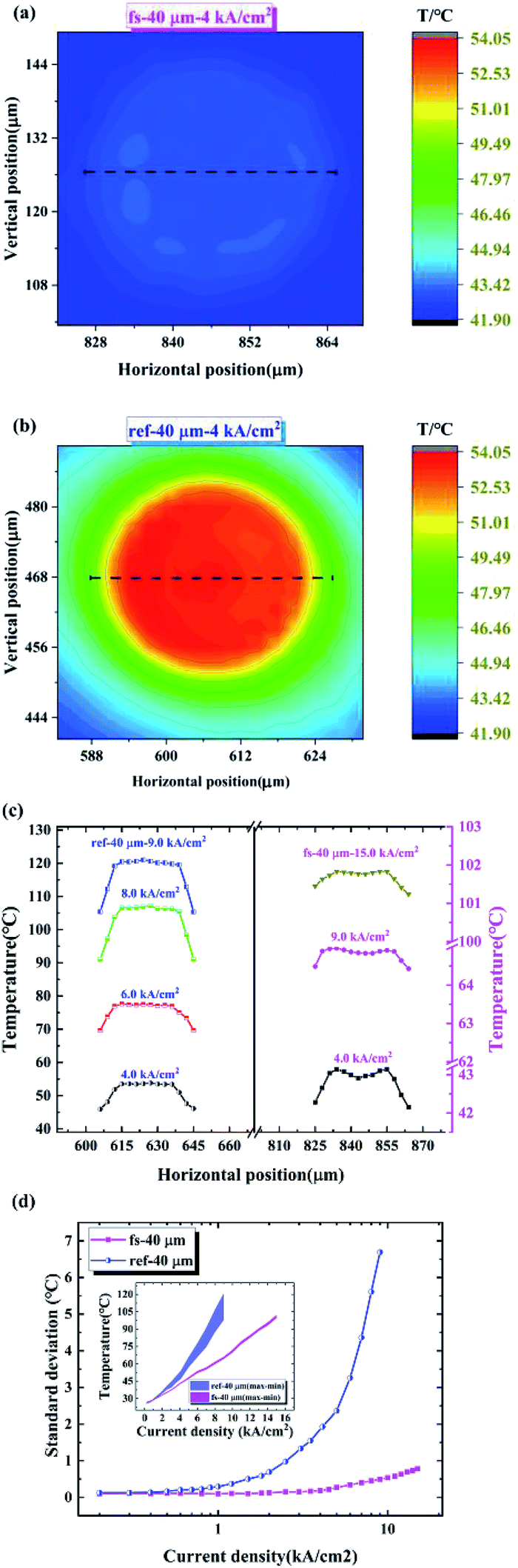 | ||
| Fig. 4 Thermal images of the (a) fs-40 μm and (b) ref-40 μm samples operated under 4 kA cm−2. (c) Several representative and (b) were operated under series of current densities. (d) Dependences of the standard deviations of the surface temperatures of 40 μm LEDs on the current injection level. The inset shows the maximum and minimum temperature values of two μLEDs and it is filled with different shadow colors. | ||
To obtain more details about the temperature distribution, we extracted the temperature data along the dashed lines in Fig. 4a and b. Fig. 4c depicts the temperatures' horizontal distribution for the fs-40 μm and ref-40 μm samples under different representative current injection levels along the dashed line. Under the same injection level, the ref-40 μm sample showed a higher temperature platform than the fs-40 μm sample. With the current density increasing, the global temperature increased similarly for both samples. However, the platform height increased rapidly for the ref-40 μm sample while it increased slowly for the fs-40 μm sample. This means that the generated heat in the junction could be rapidly dissipated to the GaN epilayers, GaN substrate, and heatsink for the fs-40 μm sample. This conformed well with the thermal transient measurement results, and it indicates that the μLED on the GaN substrate was suitable for operation under a high injection level. Moreover, an inverted “V” and an “M” corresponded to the platform shapes for the ref-40 μm and fs-40 μm samples, respectively. This may be due to the different current and thermal spreading, the simulation of which is discussed in the following section. The standard deviations (SD) of the temperature were drawn from the thermal imaging of the whole mesa, as shown in Fig. 4d. The inset shows the maximum and minimum temperature values of the two LEDs and the filled-in sections with different shadow colors show the span. The SD values of the ref-40 μm sample increased from 0.1 °C to 6.7 °C with the current density increasing from 0.1 kA cm−2 to 9 kA cm−2. For the LEDs on the GaN substrate, the SD value changed from 0.002 °C to 0.8 °C with the current density increasing from 0.1 kA cm−2 to 15 kA cm−2. Lower SD values meant more reliability because there are fewer hot spots in the devices.29,43 In the inset of Fig. 4d, the difference between the maximum and minimum is larger than the corresponding SD. The SD represents the uniformity of the temperature distribution, while the difference between the maximum and minimum indicates the local performance. Both lower SD and difference indicates the fs-40 μm sample providing higher thermal dissipation performance than the ref-40 μm sample.
In order to understand the thermal transport in μLEDs on different substrates, the temperature distributions were simulated using APSYS software. The μLEDs structure was built up according to the experimental structure. The parameters of each material were set to the defaults in the software.39 Because APSYS software could not include the thermal interface resistances directly, so we added thin layers as the interfaces and define their thermal conductivities according to the interface thermal resistances measured by thermal transient measurement. Here 1 μm-thick and low thermal conductivity GaN layer was assumed as the interface between GaN epilayer and substrate. Fig. 5a and b depicts the temperature profiles under the injection level of 4 kA cm−2 for ref-40 μm and fs-40 μm, respectively. The horizontal axis represents the lateral distance from the center on the μLED mesa. The longitudinal axis represents the distance from the substrate bottom along the growth direction. The upper red dashed lines in Fig. 5a and b show the heat source positions. The gray dashed line in the figures provides a guide for describing the typical vertical average temperature change along the diameter on the mesa. The black curves represent the isotherms for different temperatures. The total average values of Tj were about 55.89 °C and 45.21 °C for the ref-40 μm and fs-40 μm samples, respectively, which agreed with the results from the forward voltage method and the IR thermal imaging. Fig. 5c depicts the average junction temperature distribution from center to the edge on the mesa. While the PCB, Ag epoxy, and Cu heatsink still could not be added to the semiconductor model, the simulation profile was not able to show the accurate junction temperature distribution. However, the average Tj values for the μLEDs on different substrates conformed well to the experimental values. Some thermal behaviors on some parameters could be simulated by APSYS as well.
 | ||
| Fig. 5 Simulated temperature distribution of the (a) ref-40 μm and (b) fs-40 μm samples under 4 kA cm−2. The gray dashed line in the figures provides a guide for describing the average temperature changing along the mesa. The red dashed line shows the heat source position. (c) Average junction temperature distribution from center to the edge on the mesa for ref-40 μm and fs-40 μm samples. (d) Simulated current density distributions along the mesa diameter neighbor for the last QW of ref-40 μm and fs-40 μm samples under 4 kA cm−2. | ||
It was observed that the grey dashed line in Fig. 5a intersected with more isotherms than that in Fig. 5b. This means that the average Tj was less uniform for the ref-40 μm sample than that for the fs-40 μm sample. In Fig. 5c, the average temperature of ref-40 mm kept decreasing from the center to the edge of the mesa. However, the average temperature of fs-40 μm increased first and then decreased. These different trends correspond to the inverted “V” and “M” shapes in Fig. 4c. All the Tj tendencies along the diameter were similar to those in the IR thermal imaging results. To explain the simulation results, we set the TC of the sapphire substrate to the same value as that of freestanding GaN. The total average values of Tj were reduced from 55.89 °C to 45.29 °C, which were similar to the real freestanding values. The shape of the temperature platform also changed to “M” for the fs-40 μm sample. However, the isotherm densities were lower for real freestanding GaN than those for the high TC sapphire substrate. This indicates that conductive GaN made the current spreading more uniform than insulating sapphire, which caused a more uniform temperature distribution. The simulation showed that the high TC and the conductivity for the GaN substrates were the key factors for a low junction temperature and more uniform temperature distribution. To simulate more detailed temperature distribution, all the thermal interfaces and package components must be considered precisely in the future modeling and calculation.
The current density distributions of the ref-40 μm and fs-40 μm samples were simulated under a current density of 4 kA cm−2, as shown in Fig. 5c. The longitudinal axis was the ratio of the local current density for 4 kA cm−2. Uniform current spreading guaranteed the high performances for the μLEDs under a high injection level.2–4 It was found that the current density keeps increasing from the center to the edge of the mesa for both samples. The ratios of the current density at the edge of the mesa to the average one (4 kA cm−2) were 3.45 and 2.57 for the ref-40 μm and fs-40 μm samples, respectively. A higher ratio means that the current crowding was more serious. Current crowding caused the high temperature at the edge of the mesa, as seen in Fig. 5a and b. The red line represents the heat source for which the stead-state temperature distribution was similar to the current density distribution.
In this work, we measured the average junction temperature as well as the vertical and lateral thermal transport properties. The results were consistent for different methods as well as the simulation. The structure functions were used to analyze the thermal interfaces of the μLED chips. Compared with the pump and probe techniques,7,20,21 The main deficiency was the switch time of 1 μs for the heating and test currents, which shielded some signals at the very beginning. These signals were important for resolving the structure functions. It should be conquered when the switch time becomes smaller and the stability of the test circuit is improved further. The other difficulty was modeling with normal software for thermal interfaces. According to the general formalism for the interface thermal conductance, the valid models and the reliable approximation should be developed in order to obtain the accurate phonon density of states, group velocity, and so on.22
Conclusions
We investigated the thermal characteristics of μLEDs on sapphire and GaN substrates with the forward voltage method, thermal transient measurement, and IR thermal imaging. The magnitude of the K factors was smaller for smaller sized μLEDs or for GaN substrates. The junction temperature for a 40 μm μLED on the GaN substrate was about 10 °C lower than that on a sapphire substrate under a current density of 4 kA cm−2. The temperature was uniformly distributed on the GaN substrate. The thermal transient measurement showed that the spreading thermal resistances of the mesa, epilayer, and the interface of GaN/substrate were reduced significantly for μLEDs on the GaN substrate. This means that a high-quality GaN crystal and homogeneous interface corresponded to little scattering for phonons. The APSYS simulation indicated that the high thermal and electrical conductivity of the GaN substrate played a key role in the low junction temperature and uniform temperature distribution. A small-sized μLED combined with a GaN substrate can become a perfect candidate for high-power applications and visible light communication.Conflicts of interest
There are no conflicts to declare.Acknowledgements
This work was supported by the National Key Research and Development Program under Grant No. 2017YFB0403601, National Natural Science Foundation of China under Grant No. 61674005, National Natural Science Foundation of China under Grant No. 61334009, Beijing Municipal Science & Technology Commission under Grant No. Z161100001616010, Science and Technology Major Project of Guangdong Province under Grant No. 2016B010111001, and Science and Technology Planning Project of Henan Province under Grant No. 161100210200.References
- R. Ferreira, E. Xie, J. Mckendry, S. Rajbhandari, H. Chun, G. Faulkner, S. Watson, A. Kelly, E. Gu and R. Penty, IEEE Photonics Technol. Lett., 2016, 28, 2023–2026 CAS.
- S. C. Huang, H. Li, Z. H. Zhang, H. Chen, S. C. Wang and T. C. Lu, Appl. Phys. Lett., 2017, 110, 021108 CrossRef.
- Q. Q. Jiao, Z. Z. Chen, J. Ma, S. Y. Wang, Y. Li, S. Jiang, Y. L. Feng, J. Z. Li, Y. F. Chen and T. J. Yu, Opt. Express, 2015, 23, 16565–16574 CrossRef CAS PubMed.
- Z. Gong, S. Jin, Y. Chen, J. Mckendry and M. D. Dawson, J. Appl. Phys., 2010, 107, 1086 Search PubMed.
- N. L. Ploch, H. Rodriguez, C. Stolmacker, M. Hoppe, M. Lapeyrade, J. Stellmach, F. Mehnke, T. Wernicke, A. Knauer and V. Kueller, IEEE Trans. Electron Devices, 2013, 60, 782–786 CAS.
- L. Q. Yang, J. Z. Hu, L. Kim and M. W. Shin, IEEE Trans. Device Mater. Reliab., 2008, 8, 571–575 Search PubMed.
- P. E. Hopkins, ISRN Mech. Eng., 2013, 2013, 682586 Search PubMed.
- Q. M. Li, K. R. Westlake, M. H. Crawford, S. R. Lee, D. D. Koleske, J. J. Figiel, K. C. Cross, S. Fathololoumi, Z. Mi and G. T. Wang, Opt. Express, 2011, 19, 25528–25534 CrossRef CAS PubMed.
- H. S. Chen, D. M. Yeh, C. F. Lu, C. F. Huang, Y. C. Lu, C. Y. Chen, J. J. Huang and C. C. Yang, Appl. Phys. Lett., 2006, 89, 093501 CrossRef.
- A. V. Aladov, K. A. Bulashevich, A. E. Chernyakov, S. Y. Karpov, V. P. Valyukhov and A. L. Zakgeim, St. Petersburg Polytechnical University Journal: Physics and Mathematics, 2015, 1, 151–158 CrossRef.
- J. Herrnsdorf, J. J. D. McKendry, S. Zhang, E. Xie, R. Ferreira, D. Massoubre, A. M. Zuhdi, R. K. Henderson, I. Underwood and S. Watson, IEEE Trans. Electron Devices, 2015, 62, 1918–1925 CAS.
- L. Dupré, M. Marra, V. Verney, B. Aventurier, F. Henry, F. Olivier, S. Tirano, A. Daami and F. Templier, Gallium Nitride Materials and Devices XII, 2017, vol. 10104, pp. 1010422 Search PubMed.
- A. Rashidi, M. Nami, M. Monavarian, A. Aragon, K. DaVico, F. Ayoub, S. Mishkat-Ul-Masabih, A. Rishinaramangalam and D. Feezell, J. Appl. Phys., 2017, 122, 035706 CrossRef.
- A. David, N. G. Young, C. A. Hurni and M. D. Craven, Appl. Phys. Lett., 2017, 110, 253504 CrossRef.
- A. David, C. A. Hurni, N. G. Young and M. D. Craven, Appl. Phys. Lett., 2016, 109, 083501 CrossRef.
- T. A. Eckhause, Ö. Süzer, C. Kurdak, F. Yun and H. Morkoç, Appl. Phys. Lett., 2003, 82, 3035–3037 CrossRef CAS.
- J. Zou, D. Kotchetkov, A. A. Balandin, D. I. Florescu and F. H. Pollak, J. Appl. Phys., 2002, 92, 2534–2539 CrossRef CAS.
- C. Mion, J. F. Muth, E. A. Preble and D. Hanser, Appl. Phys. Lett., 2006, 89, 092123 CrossRef.
- Z. H. Su, L. Huang, F. Liu, J. P. Freedman, L. M. Porter, R. F. Davis and J. A. Malen, Appl. Phys. Lett., 2012, 100, 201106 CrossRef.
- J. Cho, D. Francis, D. H. Altman, M. Asheghi and K. E. Goodson, J. Appl. Phys., 2017, 121, 055105 CrossRef.
- J. T. Gaskins, G. Kotsonis, A. Giri, S. Ju, A. Rohskopf, Y. Wang, T. Bai, E. Sachet, C. T. Shelton and Z. Y. Liu, Nano Lett., 2018, 18, 7469–7477 CrossRef CAS PubMed.
- M. Kazan, A. Bruyant, P. Royer and P. Masri, Surf. Sci. Rep., 2010, 65, 111–127 CrossRef CAS.
- Z. X. Huang, Z. A. Tang, J. Yu and S. Y. Bai, Phys. B, 2011, 406, 818–823 CrossRef CAS.
- J. Cho, Y. Li, W. E. Hoke, D. H. Altman, M. Asheghi and K. E. Goodson, Phys. Rev. B: Condens. Matter Mater. Phys., 2014, 89, 115301 CrossRef.
- C. M. Brooks, R. B. Wilson, A. Schäfer, J. A. Mundy, M. E. Holtz, D. A. Muller, J. Schubert, D. G. Cahill and D. G. Schlom, Appl. Phys. Lett., 2015, 107, 051902 CrossRef.
- M. Hu, X. L. Zhang, D. Poulikakos and C. P. Grigoropoulos, Int. J. Heat Mass Transfer, 2011, 54, 5183–5191 CAS.
- E. Lee, E. Menumerov, R. A. Hughes, S. Neretina and T. F. Luo, ACS Appl. Mater. Interfaces, 2018, 10, 34690–34698 CrossRef CAS PubMed.
- O. Lancry, E. Pichonat, J. Réhault, M. Moreau, R. Aubry and C. Gaquière, Solid-State Electron., 2010, 54, 1434–1437 CrossRef CAS.
- B. H. Liou, C. M. Chen, R. H. Horng, Y. C. Chiang and D. S. Wuu, Microelectron. Reliab., 2012, 52, 861–865 CrossRef CAS.
- S. Y. Wen, H. L. Hu, Y. J. Tsai, C. P. Hsu, R. C. Lin and R. H. Horng, Opt. Express, 2014, 22, A601–A606 CrossRef PubMed.
- R. H. Horng, J. S. Hong, Y. L. Tsai, D. S. Wuu, C. M. Chen and C. J. Chen, IEEE Trans. Electron Devices, 2010, 57, 2203–2207 CAS.
- E. Tamdogan, G. Pavlidis, S. Graham and M. Arik, IEEE Trans. Compon., Packag., Manuf. Technol., 2018, 1–9 Search PubMed.
- G. Xueqin, F. Shiwei, Y. Yuan, Y. Junwei and L. Jingwei, J. Semicond., 2016, 37, 044011 CrossRef.
- Y. Xi and E. F. Schubert, Appl. Phys. Lett., 2004, 85, 2163–2165 CrossRef CAS.
- P. C. Tsai, R. W. Chuang and Y. K. Su, J. Lightwave Technol., 2007, 25, 591–596 Search PubMed.
- J. L. Zhan, Z. Z. Chen, Q. Q. Jiao, Y. L. Feng, C. C. Li, Y. F. Chen, Y. Y. Chen, F. Jiao, X. N. Kang and S. F. Li, Opt. Express, 2018, 26, 5265–5274 CrossRef CAS PubMed.
- E. I. Association, EIA/JEDEC Standard, JESD51-1, 1995 Search PubMed.
- APSYS (2018 version), Crosslight Software, Inc., Burnaby, Canada, http://www.crosslight.com Search PubMed.
- D. A. Browne, B. Mazumder, Y. R. Wu and J. S. Speck, J. Appl. Phys., 2015, 117, 185703 CrossRef.
- L. Jun Ze, T. Yue Bin, C. Zhi Zhong, J. Xian Zhe, F. Xing Xing, J. Shuang, J. Qian Qian, Y. Tong Jun and Z. Guo Yi, Chin. Phys. B, 2013, 23, 016101 Search PubMed.
- E. Y. Xie, Z. Z. Chen, P. R. Edwards, Z. Gong, N. Y. Liu, Y. B. Tao, Y. F. Zhang, Y. J. Chen, I. M. Watson and E. Gu, J. Appl. Phys., 2012, 112, 013107 CrossRef.
- M. Rencz and V. Székely, Twentieth Annual IEEE Semiconductor Thermal Measurement and Management Symposium, IEEE Cat. No. 04CH37545, 2004, pp. 50–54 Search PubMed.
- Z. Z. Chen, P. Liu, S. L. Qi, L. Lin, H. P. Pan, Z. X. Qin, T. J. Yu, Z. K. He and G. Y. Zhang, Mater. Sci. Semicond. Process., 2007, 10, 206–210 CrossRef CAS.
| This journal is © The Royal Society of Chemistry 2019 |