
 Open Access Article
 This Open Access Article is licensed under a Creative Commons Attribution-Non Commercial 3.0 Unported Licence
Electronic performance of printed PEDOT:PSS lines correlated to the physical and chemical properties of coated inkjet papers†
Viviane Forsberg *abc,
Jan Mašlíkd and
Magnus Norgrena
*abc,
Jan Mašlíkd and
Magnus Norgrena
aMid Sweden University, FSCN, Surface and Colloid Engineering, Holmgatan 10, SE-851 70, Sundsvall, Sweden. E-mail: viviane.forsberg@miun.se
bKTH Royal Institute of Technology, Department of Fiber and Polymer Technology, Biocomposites Division, Teknikringen 56, SE-100 44, Stockholm, Sweden. E-mail: vivforsb@kth.se
cWallenberg Wood Science Centre, Teknikringen 56, SE-100 44, Stockholm, Sweden
dTomas Bata University in Zlín, Centre of Polymer Systems, Trida Tomase Bati 5678, CZ-760 01, Zlín, Czech Republic
First published on 1st August 2019
Abstract
PEDOT:PSS organic printed electronics chemical interactions with the ink-receiving layer (IRL) of monopolar inkjet paper substrates and coating color composition were evaluated through Raman spectroscopy mapping in Z (depth) and (XY) direction, Fourier transform infrared spectroscopy (FTIR) and energy dispersive X-ray spectroscopy (EDS). Other evaluated properties of the IRLs were pore size distribution (PSD), surface roughness, ink de-wetting, surface energy and the impact of such characteristics on the electronics performance of the printed layers. Resin-coated inkjet papers were compared to a multilayer coated paper substrate that also contained an IRL but did not contain the plastic polyethylene (PE) resin layer. This substrate showed better electronic performance (i.e., lower sheet resistance), which we attributed to the inert coating composition, higher surface roughness and higher polarity of the surface which influenced the de-wetting of the ink. The novelty is that this substrate was rougher and with somewhat lower printing quality but with better electronic performance and the advantage of not having PE in their composite structure, which favors recycling.
Introduction
Three scientists, Shirakawa, MacDiarmid and Heeger, presented their breakthrough research on conducting polyacetylene doped with halogens in 1977.1 Nowadays, polyacetylene is known as a prototype conducting polymer and can be p- and n-doped chemically or electrochemically.2 This discovery was recognized with the Chemistry Nobel Prize in 2000.3 Studies of a number of different conducting polymers were an inevitable development after their discovery.4,5 Water-soluble conducting co-polymers poly(3,4-ethylenedioxythiophene)–poly(styrene sulfonic acid) (PEDOT:PSS) discovery occured in 1995,6 and a number of other studies around this polymer emerged thereafter.7–9PEDOT is insoluble, but when PSS, a water-soluble poly-electrolyte is used as a counter ion, the system is stabilized.10 Today, all printed transistor circuits are possible using only organic polymers11 and more recently two-dimensional materials.12,13 Vapor-phase polymerization is one of the available processes to produce conducting polymers using FeCl3 or H2O2 as oxidizing agents.10 The great advantage of solution-processable polymers is that they can easily be printed with commercially available inkjet printers with minimal usage of material and achieve conductive path lines with very few printing passes.14
To date, there are many efforts to replace materials that are becoming less readily available, which impacts commercial costs such as indium tin oxide (ITO)15 with materials that can be used in flexible displays. A telephone screen that does not break will certainly appear more appealing than the technology available nowadays.
Thin-film transistors (TFTs) of layered materials using graphene or MXenes as conductors, phosphorene, molybdenum disulfide or other layered transition metal dichalcogenides as semiconductors and boron nitride or silicates as insulators have been reported,12,13,16,17 and although they perform better than organic electronics in terms of electron mobility (i.e., >10 cm2 V−1 s−1) and have remarkable mechanical and electronic properties due to quantum confinement when the layers of the materials are exfoliated,18–22 there are still limitations to using these materials in flexible devices. The high intrinsic mobility23 also demands additional engineering steps at the junctions to improve mobility.22
Organic electronics, on the other hand, have clear advantages compared to layered materials for low power electronics. Flexible and with high conductivity in the order of 4.6 S cm−1 when doped with PSS into a conductive state,24,25 PEDOT is one of the most used conductive polymers nowadays. PEDOT has both high electronic and high ionic conductivity. The fact that it has high electrical conductivity and low thermal conductivity makes it a potential candidate for thermoelectric generators,26 which can be quite useful for self-powered sensors.
The substrates used for printed electronics have primarily been plastics, but the alarming consequences of the unsustainable use of these materials necessitate action particularly highlighted by the Sustainable Development Goals adopted by the United Nations for 2030.27 Biodegradable electronics28 could help to reduce the impact of discarded electronics waste that has become a problem causing pollution of soil and water especially when the costs for electronics are so low.25
With the advances of the Internet of Things (IoT) becoming more and more a reality and with embedded automation and smart systems integration, trillions of sensors will be needed to enable artificial intelligence.29 With this, the need for devices that are self-powered and cheap has also become a drive to develop technologies to enable the use of sustainable, flexible substrates.
The use of paper as a substrate for this purpose has numerous advantages because paper is a cheap commodity material and the paper industry is capable of supplying enough surface area for printed electronics in a month, which would take the silicon-based industries a year to achieve.30 Some paper grades may have higher surface roughness than plastics like PE. This roughness may be reduced with surface coating and calendering. Ihalainen et al.31 presented a study of the influence of paper roughness on the electrical performance of printed wires using silver nano-particles and organic polymer (i.e., polyaniline) inkjet inks and found a linear correlation between resistance and short length roughness of the print substrates.
Porous IRLs are thick layers (i.e., 30 < h < 50 μm),32 and only a very small swelling of the binders contributes to the total ink absorption, and all of the ink must be absorbed by the pores formed between the pigments and within the pigments. Substrates contained the PE layer were designed to have the thick IRL to absorb all the ink solvent while ensuring good wetting and printing quality for inkjet papers. The PE layer also reduces the roughness considerably31 as it will be discussed shortly.
For inkjet printing, according to Kettle et al.,33 there are seven interaction phenomena that coexist during the inkjet ink absorption process. Wetting occurs as soon as the droplet hits the paper surface. At the same time, the capillary forces start to act, forcing the ink to penetrate the IRL; this happens at around 0.1 ms after the droplet has contacted the surface.34,35 After a few milliseconds, the separation of the ink components starts taking place and the capillary penetration continues strongly. Adsorption increases after 1 s. Diffusion starts at the capillary's ink penetration and increases with time when the ink has penetrated deeper into the coating structure. Finally, the last two phenomena that occur during ink absorption after the inkjet printing process are polymerization and drying. Polymerization, for inks which have the ability to polymerize, takes at least 100 s to start occurring, and the final drying rate of the ink can be in the range of hours.33
Understanding high-performance paper substrates, especially the coating layers (CLs) of the IRLs of these substrates regarding the porous structure,33 coating color composition, roughness,31,36 the mechanisms of ink penetration,33 ink de-wetting37,38 and the impact of such characteristics on the electronics performance of the substrates, could provide a direction for product development of grades to enable better electronics performance, especially for printing with organic conductive inks. With this in mind, we investigated the effects of different substrates on printability and electrical resistance.
Six substrates were carefully characterized and subjected to inkjet printing using a water-based ink containing PEDOT:PSS. Ink distribution was characterized using Raman spectroscopy and SEM, considering de-wetting phenomena. Effects from ink distribution on electrical resistance of the printed lines were analyzed. We evaluated that even though rough substrates lead to poorer printability, the electrical resistance is lower because the roughness will create areas with thicker ink layers than others, lowering the sheet resistance in some places. The printability could be improved by surface treatment of such substrates with silanization.39,40
Experimental
Inkjet printing of the conductive lines
The substrates were printed using a commercially available PEDOT:PSS water-based ink with 0.8 wt% (Orgacon IJ 1005, Sigma Aldrich), surface tension of 24 mN m−1 (Krüss, K6), and pH of 1.5–2.5. A Dimatix 2831 printer and Dimatix 11610 cartridges with 10 pL drop volume were used to print the contact lines. The template was printed using 20 μm drop spacing, which corresponds to a resolution of 1270 dpi. The conversion of centimeter to pixel can be done using the factor xR/2.54, where x is the length in centimeter, R the resolution in dots per inch and 2.54 is a conversion factor, the thickness of the printed lines in micrometer will be described in the text.The template used for the electronic analyses with 2-probes was printed using four nozzles and one printing pass. The waveform used was the one supplied by the manufacturer for distilled water with no alterations. For the Raman measurements and 4-probe sheet resistance analyses, the 20 pixel lines of the template were printed three-times and the measurements were done on the contacts areas for the Raman and on the lines for the sheet resistance. We used 1 nozzle to print these patterns.
Estimation of the surface roughness of the substrates
We evaluated the surface roughness through AFM measurements on a 50 μm2 area of the substrates using a Dimension ICON (Bruker) instrument working in a PeakForce with ScanAsyst-Air probe without a controlled environment. The surface roughness was calculated using the software NanoScope Analysis.SEM analyses of the morphology of the pores in the IRLs
We obtained SEM images (TESCAN MAIA3, Triglav) of the top surface of the substrates at 39![[thin space (1/6-em)]](https://www.rsc.org/images/entities/char_2009.gif) 500× magnification, acquired at 2 keV at the working distance of ≈7 mm with a SE detector in ultra high-resolution mode (UHR). The morphology tool of the software was employed to estimate PSD through imaging processing. Samples were cut into small squares and attached to an aluminum stub using double-sided coated carbon tape. Silver conductive ink was applied at the edges of the sample, once dried, they were coated with 5 nm iridium (Q150T ES, Quorum) to avoid electrostatic charging of the samples.
500× magnification, acquired at 2 keV at the working distance of ≈7 mm with a SE detector in ultra high-resolution mode (UHR). The morphology tool of the software was employed to estimate PSD through imaging processing. Samples were cut into small squares and attached to an aluminum stub using double-sided coated carbon tape. Silver conductive ink was applied at the edges of the sample, once dried, they were coated with 5 nm iridium (Q150T ES, Quorum) to avoid electrostatic charging of the samples.
Coating composition analyses through EDS
Cross-section SEM images (TESCAN MAIA3, Triglav) of the substrates embedded in slow-curing transparent epoxy resin (Epofix Kit, Struers) were taken to perform the EDS analyses.Initially all samples were attached into an aluminum spring and the resin deposited into a Teflon container using a vacuum chamber. The spring was removed by pulling it, and the samples polished. The embedded samples were polished following a protocol with a sequence of sand papers (#320, #500, #1200, #4000, Largo 6 μm, Dur 3 μm and Nap 1 μm, Struers). We ran the equipment for ≈4 min using water for the coarser grades (#320 and #500) and for ≈2 min for the finer ones using DP lubricant (TegraPol-21 equipped with a Tegra Doser-5, Struers).
The embedded samples attached to the aluminum stub are illustrated in Fig. 1. The sample was coated with 5 nm chromium and accessed right after to avoid the oxidation of the coating. Images were accessed using backscattered electron detector (BSE) in analysis mode at 20 keV. The EDS detector (Oxford Instruments accessory X-Max 50) was coupled with the SEM equipment, and the Aztec software was used for data acquisition and analyses.
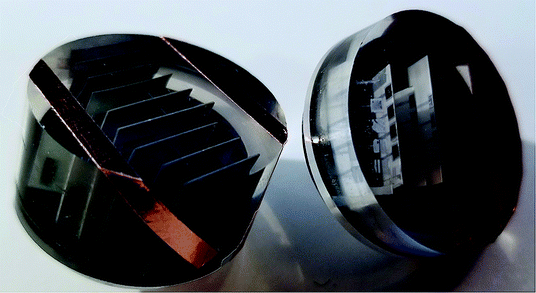 | ||
| Fig. 1 Photograph of the embedded samples in resin for the SEM-EDS cross section analyses. | ||
Coating composition analyses through FTIR
FTIR (Nicolet 6700 FT-IR) spectra of the substrates were taken using the instrument's attenuated total reflectance (ATR) mode. Before acquisition of spectra, we purged the instrument for 30 min with nitrogen to attenuate the spectral contribution from atmospheric water and carbon dioxide. The spectra were acquired with 64 scans and resolution 2 (i.e., 0.964 cm−1).Contact angle measurements to estimate surface energy parameters
Contact angle measurements to determine the surface energy on the substrates were performed using the Advex instrument. Measurements were taken at 23 °C room temperature. We used 3 μL of the liquids, and the images were taken a few seconds after drop contact to the surface until the drop geometry was stabilized. Each measurement was repeated 5 times.Ink distribution and ink-substrate chemical interactions
We used Raman spectroscopy (Horiba Xplora Plus) to evaluate the chemical interactions ink-substrate in the YZ direction and to map the surface in the XY direction. Both analyses were done in the XYZ direction to determine the focus point; the differences in the measurements were the number of data points and increment. These measurements were performed in confocal mode at 100 μm, using a 100× objective (Olympus MPlan) with numerical aperture equal to NA = 0.90. The excitation wavelength of the laser was 532 nm, with a 600 nm groove, a slit width opening of 100 μm and 1% laser power (i.e., 2.5 mW) to avoid overheating of the substrates. Acquisition time was 20 s, and there were 3 accumulations (i.e., average of three spectra for each point). The spectral pixel resolution (i.e., the sampling interval of the spectrum) was 0.4 cm−1.We also performed FTIR on the top of the printed lines and the substrates to evaluate the chemical interactions between the substrate and the ink. This was done on the outermost surface of the ink. The Raman spectroscopy analyses complemented these analyses in depth into the sample in Z direction.
Electrical properties of printed lines
The electrical properties of the printed lines were evaluated for different line thicknesses and sintering temperatures using a bench multimeter (34410A 6.5, Agilent) with two probes but also performed analyses of sheet resistance using a four-probe measurement device unit type G, tip R 100 μm, force 100 g. The probes were equidistant 0.635 mm (Jandel), these were coupled with a bench multimeter (2611A Keithley).Results and discussion
This section is divided into three parts. Part one refers to the physical and chemical characterization of the surface of the substrates S1 to S6 in terms of PSD, surface roughness, the composition of the CLs in the IRLs of the substrates and the contact angle measurements to estimate the surface energy. Part two is related to the printed PEDOT:PSS lines, the ink distribution (de-wetting) on the surface of the substrates and the analyses of ink-substrate chemical interactions. Part three is related to the electrical properties of the printed lines and how the results from Part one and Part two help us to answer the research question regarding the impact on the ionic/electronic performance of the PEDOT:PSS printed lines depending on the substrate chemical and physical characteristics. We end this section with some references to electronics applications performed on some of the substrates analyzed in this study. A summary of the results for the characterization of the substrates is indicated in Table 1.| Substrate | L1 [μm] | L2 [μm] | L3 [μm] | BP [μm] | Main coating component of the IRL | Sq [nm] | γS [mN m−1] |
|---|---|---|---|---|---|---|---|
| S1 | (CL1) 3.4 ± 0.1 | (CL2) 17 ± 0.4 | (CL3) 9.8 ± 1.3 | 62 ± 2.8 | (CL1) SiO2; (CL2) AlO(OH) and (CL3) CaCO3 | 105 | 66 |
| S2 | (CL1) 42 ± 0.4 | (PE) 19 ± 2.8 | NA | 153 ± 2.8 | AlO(OH) | 11 | 58 |
| S3 | (CL1) 37 ± 0.6 | (PE) 31 ± 2.1 | NA | 170 ± 3.3 | SiO2 | 11 | 55 |
| S4 | (CL1) 35 ± 0.7 | (PE) 31 ± 0.4 | NA | 167 ± 2.0 | SiO2 | 12 | 55 |
| S5 | (CL1) 5 ± 0.2 | (CL2) 38 ± 0.2 | (PE) 33 ± 1.5 | 190 ± 2.0 | (CL1) AlO(OH) and (CL2) SiO2 | 16 | 61 |
| S6 | (CL1) 0.5 ± 0.02 | (CL2) 42 ± 0.7 | (PE) 23 ± 1.3 | 173 ± 1.0 | (CL1) AlO(OH) and (CL2) SiO2 | 12 | 53 |
Part 1: physical and chemical surface characterization of the substrates
To access the chemical composition of the CLs, we used two methods: FTIR and EDS. These methods complemented one another. The resolution limitation of the different techniques used in this study are explained in the ESI.†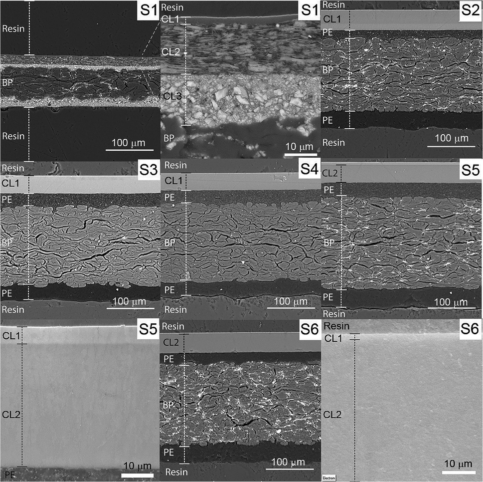 | ||
| Fig. 2 Cross-section SEM images of the substrates accessed at 20 keV at working distance ≈ 7 mm in UHR mode using a BSE to improve contrast. Where the scale is 10 μm, the images were taken at a view-field of 50 μm and acquired in analysis mode using a SE detector. The CLs are indicated in the image as well as the PE and BP composite layers. Resin refers to the embedded material of the sample. A thin gold layer 4 nm was sputtered on the top of the sample to help distinguish between the CL and the resin interface. | ||
S1 was provided by Åbo Akademi and contain 3 CLs. It was produced in laboratory scale and was also calendered. S2 to S6 are resin-coated substrates all containing an extruded pigmented PE layer on the top and a non-pigmented PE on the back of the BP. On the top of the PE layer there is the IRL containing one CL for S2, S3 and S4 and two CLs for S5 and S6.
The total surface mapping was performed in the entire cross-section images that are illustrated in color in Fig. 3 on top of the EI. The atomic composition in percentage and the spectra of the CLs measured for the area scans are presented in Fig. 4, the thickness of the layers are also indicated. For the surface mapping of the cross-section these results are presented in the ESI Fig. S1.†
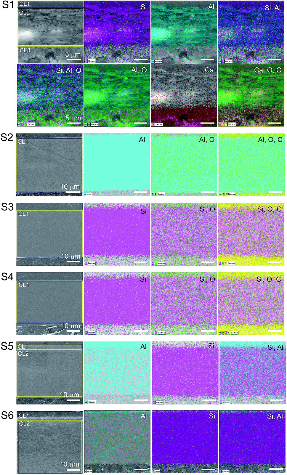 | ||
| Fig. 3 EDS mapping of the cross-section surfaces of the substrates. The areas surrounded by yellow in the EI were the regions used for the area scan. The scales of the images are the same as that of the first image on the line. The elements identified in the mapping are indicated in the image as silicon (Si), aluminum (Al), oxygen (O), calcium (Ca) and carbon (C). The elemental spectra and atomic percentage of the mapping is presented in the ESI.† | ||
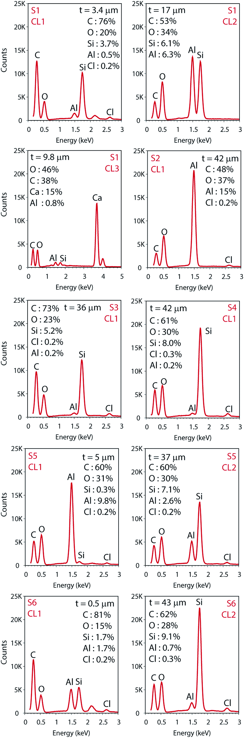 | ||
| Fig. 4 Area scan spectra for the coated IRLs. The top coat (CL1), second (CL2) and third (CL3) coated layers are indicated. The thickness of the layer (t) is indicated in μm and the elemental-atomic percentage of the main components is indicated. | ||
Elemental Si and Al were identified in the EDS analyses which is in agreement with the FTIR analyses for boehmite [AlO(OH)] and silica (SiO2). Some substrates contained both pigments in their IRL coating composition. For S1 we note a 3.4 μm silica layer in CL1 constituted of mainly Si (i.e., 3.7%) followed by a 17 μm CL2 constituted of highly oriented platy pigments containing alumina and silica at slightly the same atomic percentage proportion (i.e., 6.1 and 6.3% for Si and Al respectively), and a 9.8 μm CL3 containing mainly Ca (i.e., 15%), which we attribute to the presence of CaCO3 with broad particle size distribution. S2, S3 and S4, contain only one pigment in the CL1 (i.e., elemental Al in S2 and Si for S3 and S4).
The analyses of the accuracy of the EDS measurement was done through the evaluation of the background. The background is the curved baseline at the bottom of the spectra (see Fig. 4). A rule of thumb is that the data are detectable if 3 times the square root of the peak height is higher than the background. If this condition is not fulfilled, the data are not detectable and could appear as noise. When evaluating the surface mapping shown in Fig. 3, there are some regions colored outside the IRL region which we know is due to noise. The principal X-ray emission lines are indicated in Table S1 in the ESI.†
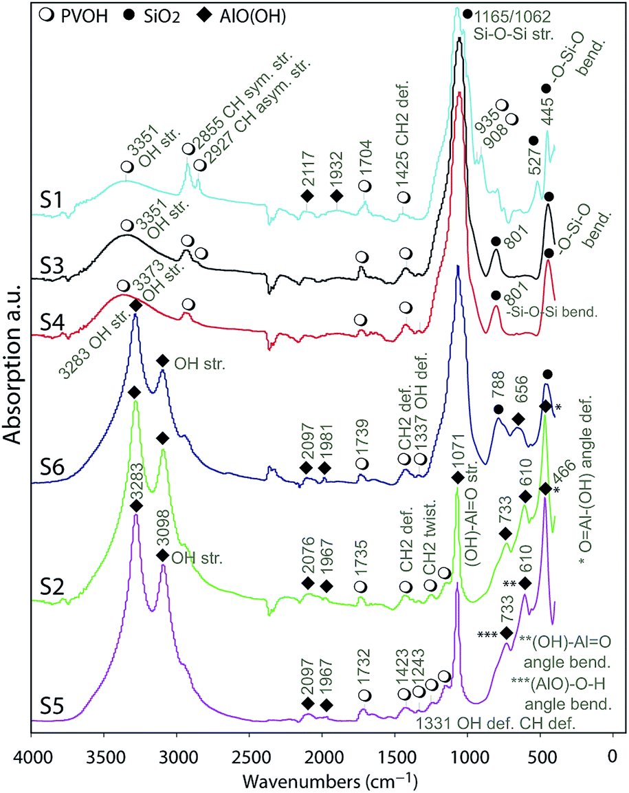 | ||
| Fig. 5 FTIR analyses on the surface of the substrates indicating the presence of AlO(OH), silica and PVOH referred by icons in the legend. | ||
The analyses of the spectra indicated the appearance of symmetric and asymmetric stretching IR vibrations in OH groups41 at 3098 and 3286 cm−1 for the substrates S2, S5 and S6 indicating the presence of AlO(OH) in their IRLs. There are 6 fundamental modes (FMs) of vibration in a 4-atom nonlinear molecule as AlO(OH); these are well illustrated in the literature.42 Assuming AlO as a single-point mass the OH group's IR vibrations can be described as OH group stretching, (AlO)–O–H angle bending and (AlO)–O–H deformation.
The other three FMs of vibration can be described as (OH)–Al![[double bond, length as m-dash]](https://www.rsc.org/images/entities/char_e001.gif) O symmetric bond stretching, (OH)–AlO angle bending and (OH)–AlO asymmetric bond stretching.42 Well-resolved absorbance bands were observed in the region from 400 to 1200 cm−1. Taking, for example, S2, these bands were at 466, 610, 733, 1071 and 1147 cm−1. At 1071 cm−1, a sharp and strong band is assigned to the (OH)–AlO asymmetric stretching vibration, and the small shoulder at 1147 cm−1 is related to the O–H bending. The (AlO)–O–H angle bending is indicated by the 733 cm−1 band and the (OH)–AlO angle bending is attributed to the band at 610 cm−1. The sharp band at 466 cm−1 is attributed to the angle deformation (wagging) of OAl–(OH). The bands in the region 1500 to 2500 cm−1 are relatively weaker compared to those in the other regions. The broader peak at 1165 cm−1 for S6 indicate the presence of silica in the IRL as it was discussed previously on the EDS analyses.
O symmetric bond stretching, (OH)–AlO angle bending and (OH)–AlO asymmetric bond stretching.42 Well-resolved absorbance bands were observed in the region from 400 to 1200 cm−1. Taking, for example, S2, these bands were at 466, 610, 733, 1071 and 1147 cm−1. At 1071 cm−1, a sharp and strong band is assigned to the (OH)–AlO asymmetric stretching vibration, and the small shoulder at 1147 cm−1 is related to the O–H bending. The (AlO)–O–H angle bending is indicated by the 733 cm−1 band and the (OH)–AlO angle bending is attributed to the band at 610 cm−1. The sharp band at 466 cm−1 is attributed to the angle deformation (wagging) of OAl–(OH). The bands in the region 1500 to 2500 cm−1 are relatively weaker compared to those in the other regions. The broader peak at 1165 cm−1 for S6 indicate the presence of silica in the IRL as it was discussed previously on the EDS analyses.
Taking, for example, S1, S3 and S4, the assignments of the absorption bands at 445 cm−1, 801 cm−1, 1062 cm−1 and 1140 cm−1 are well-known assignments to the vibrations of the tetrahedral –SiO4 groups.43,44 The two components at 1165 cm−1 and 1062 cm−1 are due to the 3-fold degenerated Si–O–Si asymmetrical stretching frequencies of the tetrahedral –SiO4 structural unit. The absorption band around 801 cm−1 is due to –Si–O–Si bending modes, while the one at 445 cm−1 is due to –O–Si–O bending.45 The bands around 3351 cm−1 are due to –OH stretching,44 while the bands at 2855 cm−1 and 2927 cm−1 are due to CH symmetrical and asymmetrical stretching related to the vibrations of the PVOH molecule.
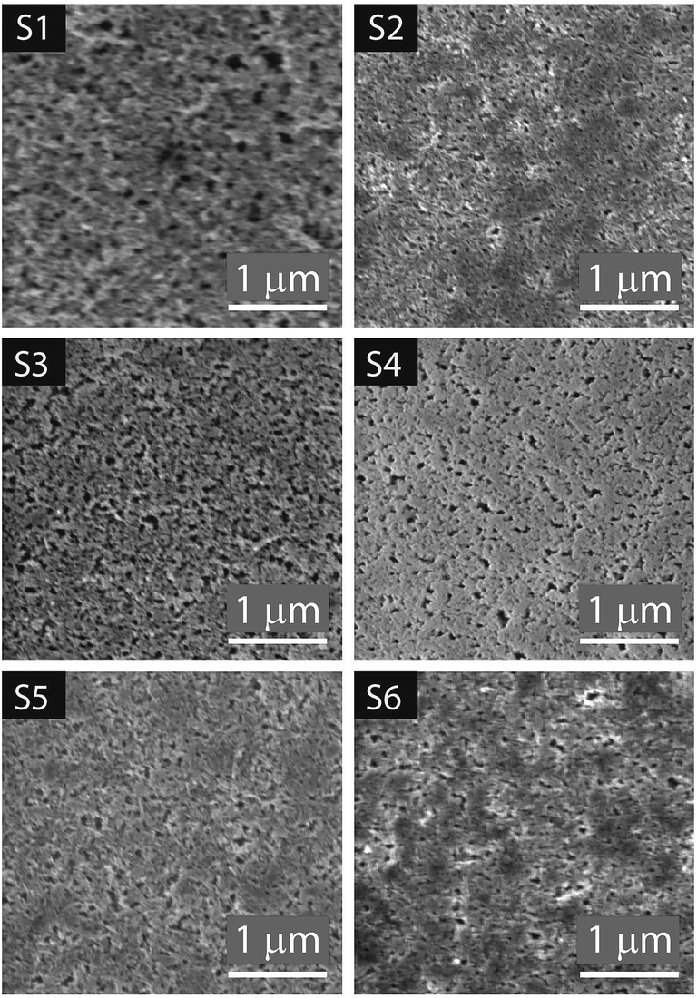 | ||
| Fig. 6 SEM images of the top surface of the substrates at 39500× magnification with the scale indicating 1 μm, view field 3.5 μm accessed at 2 ke V. | ||
The IUPAC system classifies pores according to the diameter (D) as follows: micropores, <2 nm; mesopores, 2 < D < 50 nm; and macropores > 50 nm.47 In Fig. 7A the analyzed pores are highlighted in yellow. The length and width of the pores are presented in the histograms in Fig. 7B and C respectively. Most of the porous IRLs have pores in the macropores range. S1 and S3 have broader PSD. S3 is the most porous substrate with a significantly higher number of pores compared to the other substrates. The main differences between these two substrates would be the thickness of each CL, the absence of the PE layer for S1 and the composition of the CL that was discussed in the previous section.
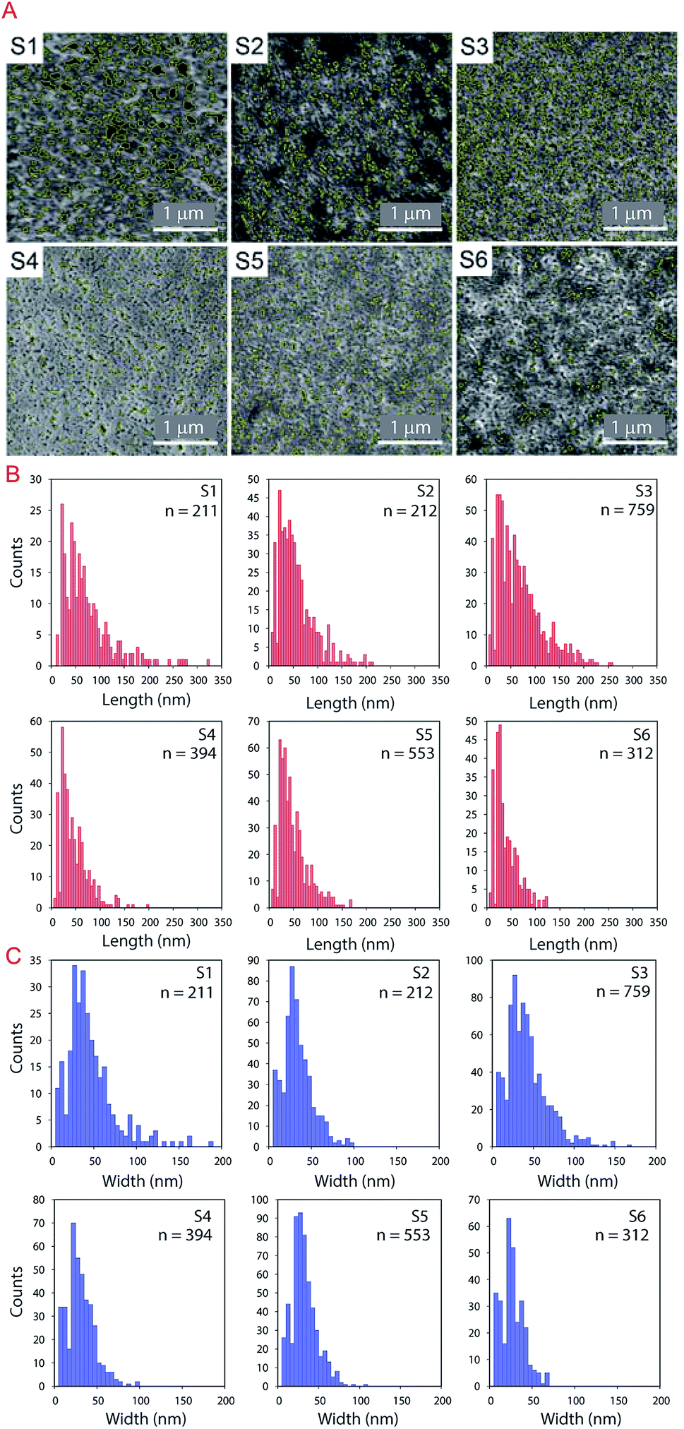 | ||
| Fig. 7 PSD analyses by processing SEM images (A) indication of the analyzed pores highlighted in yellow on the top of the substrates. The analyses were done using the image processing tool morphology of the software from the SEM instrument. (B) Histograms of the PSD after morphology analyses considering the length and (C) the width of the pores; n indicates the number of pores analyzed. | ||
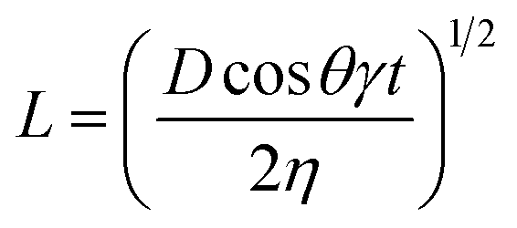
It is common to refer to the Lucas–Washburn48 equation (eqn (1)) to discuss penetration of fluids into porous media.
 | (1) |
In this equation, the length (L) of the ink penetration is directly proportional to the square root of the pore diameter (D), where γ is the surface tension of the liquid, η is the dynamic viscosity, t is time of the fluid penetration in seconds and θ is the contact angle. This means the bigger the pores, the faster the ink solvent penetration. However, the pores should not be bigger than the ink particles because it is the ink solvent's fast penetration that is important, and as little as possible of the pigment to penetrating the IRL is ideal. The bigger pores in S1 contribute to a faster ink absorption and penetration which cause poor printability but the fact that it was a rougher substrate has contributed to a better wetting of the surface as it will be discussed shortly.
The porous network of the paper coatings have not been evaluated in this study, the technique used for this purpose is usually mercury porosimetry together with software simulations. We would like to refer the reader to the extensive work from Gane et al.,49 Ridgway et al.50,51 and co-authors in this subject.
|
γL(1 + cosθ) = 2[(γLWSγLWL) + (γS+γL−) + (γS−γL+)]1/2
| (2) |
| Liquid | γL [mN m−1] | γLWL [mN m−1] | γABL [mN m−1] | γL+ [mN m−1] | γL− [mN m−1] |
|---|---|---|---|---|---|
| Water | 72.8 | 21.8 | 51 | 25.5 | 25.5 |
| Diiodomethane | 50.8 | 50.8 | 0 | 0 | 0 |
| Ethylene glycol | 48 | 29 | 19 | 47.0 | 1.92 |
| Substrate | Diiodomethane | Ethylene glycol | Water | Ink |
|---|---|---|---|---|
| S1 | 19.7° | 20.1° | 19.7° | 35.6° |
| S2 | 31.5° | 34.7° | 38.8° | 50.1° |
| S3 | 23.8° | 28.1° | 43.0° | 56.4° |
| S4 | 23.4° | 23.3° | 37.3° | 47.3° |
| S5 | 23.8° | 33.1° | 40.1° | 51.0° |
| S6 | 33.1° | 37.0° | 46.0° | 43.4° |
Busscher et al.54 report a polar component for the surface energy of diiodomethane (methylene iodide) (i.e.; γLWL = 47.4 mN m−1 and γABL = 2.6 mN m−1) we noticed this after performing our measurements. α-Bromonaphthalene is a liquid with only dispersive components and could be used instead for better accuracy. The overall surface energy (γS) is a sum of the dispersive (γLWS) and the polar component (γABS) of the surface energy. We also wish to point out that the ambient temperature during the experiment influence the contact angle and that the higher the temperature the lower the surface tension. The values described in Table 2 are at 20 °C and would be lower at the temperature of 23 °C, the ambient temperature where the measurements were carried out.
The resulting surface energy data are listed in Table 4. They were obtained from the instrument software that used eqn (2) to determine the parameters of the surface energy of the substrates. All substrates show a strong electron donor γS− (Lewis base) and a negligible electron acceptor γS+ (Lewis acid) indicating a very asymmetric polarity characteristic to monopolar surfaces, according to Van Oss.52 Due to the polar component of the surface energy (i.e., γAB = 18 mN m−1) being slightly higher than the other substrates, the substrate S1 is more favorable to wetting of a polar ink than the other substrates; as a result we observed a lower contact angle measured for the ink on this substrate 35.6° compared to the others (see Table 3).
| Substrate | γS [mN m−1] | γLWS [mN m−1] | γABS [mN m−1] | γS+ [mN m−1] | γS− [mN m−1] |
|---|---|---|---|---|---|
| S1 | 65.8 | 47.9 | 18.0 | 1.1 | 74.5 |
| S2 | 57.7 | 43.6 | 14.1 | 0.9 | 58.4 |
| S3 | 54.7 | 46.6 | 8.1 | 0.4 | 45.9 |
| S4 | 55.3 | 46.7 | 8.6 | 0.3 | 52.1 |
| S5 | 61.3 | 46.6 | 14.8 | 1.0 | 54.9 |
| S6 | 53.1 | 42.9 | 10.1 | 0.5 | 47.6 |
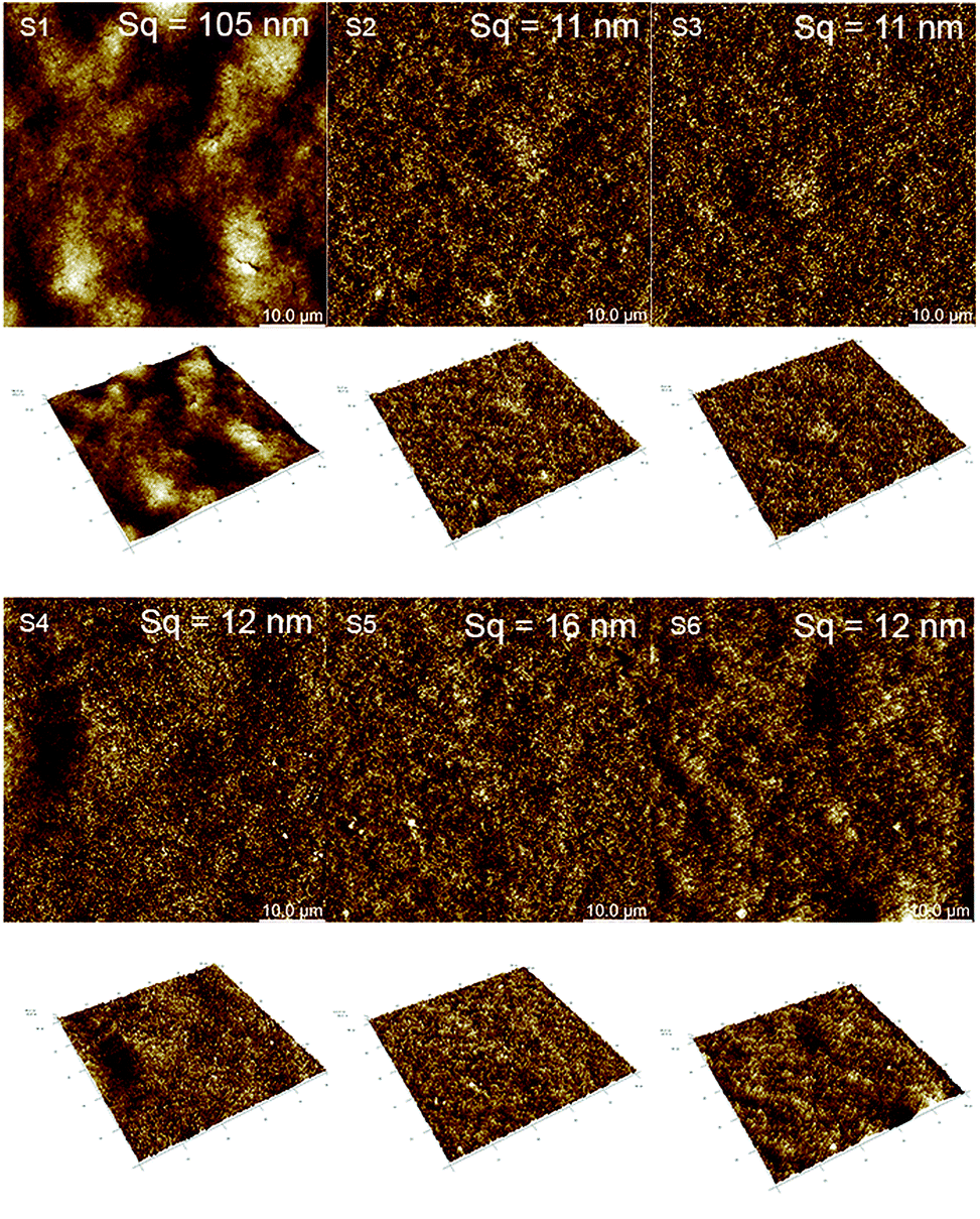 | ||
| Fig. 8 RMS surface roughness analyses of the substrates accessed by AFM. The legend indicate 10 μm. | ||
There are basically two wetting regimes for rough substrates: homogeneous and heterogeneous.56 The difference between them is that in the first the liquid fill the roughness grooves and in the second air would fill the grooves. For homogeneous wetting regimes the Wenzel equation apply as for the second, Cassie–Baxter apply.56 Wetting is enhanced by roughness for homogeneous regimes according to the Wenzel equation if the contact angle is smaller than 90° and hampered if the contact angle is higher than this value.57
Samyn et al.36 also pointed out in their studies that for an intrinsically hydrophilic material, the wetting will be amplified the higher the number of asperity sites. We observe this effect for S1, a rougher substrate compared to the others with significantly better wetting performance.
The roughness of the substrate may also influence the result of the contact angle measurement as it does the drop volume of the test liquid and the time required for the drop to stabilize in the surface.58 From a study presented by Busscher et al.,54 if the surface roughness is below 100 nm it does not impact the contact angle result. The substrates analyzed in this study have surface roughness below this value except S1 (i.e.; 105 nm) but with a value very close to this threshold. For this reason we did not consider the Wenzel equation that take into account the surface roughness to correct the contact angle results as it was done by Ihalainen et al.31
Part 2: PEDOT:PSS ink distribution on monopolar substrates and chemical interactions ink/substrate
The analyses of the coating composition is important specially when we wish to verify the inertness of the substrates. Chemical reactions between the substrate IRL and the printed ink layer would appear in the analyses of the FTIR illustrated in Fig. 9. These spectra were acquired from the surface of a 20 pxl printed line with 3 printed layers (PLs) of the ink and from the surface of the substrate without the printed lines. From these data we can evaluate the inertness of the substrates to the PEDOT:PSS ink, as there is no indication of a chemical reaction verified by the fact that the spectra for the ink are similar in all substrates. Note that the region for the fingerprint of the PEDOT:PSS is in the range of 900 cm−1 to 1700 cm−1 similar to what is presented for the Raman in Fig. 10A. The PEDOT:PSS chemical structure is presented in Fig. 10B.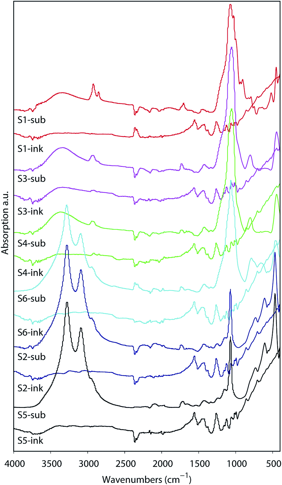 | ||
| Fig. 9 FTIR for the substrate and the printed PEDOT:PSS ink layer. The measurement for the ink was done on the surface of a 20 pxl printed line with 3 PLs of the ink while the spectra for the substrate was acquired on the surface of the substrate. Sx-sub indicate the spectra for the respective substrate where x is the number of the substrate from 1 to 6. Sx-ink indicate the spectra of the printed ink on the respective substrate. | ||
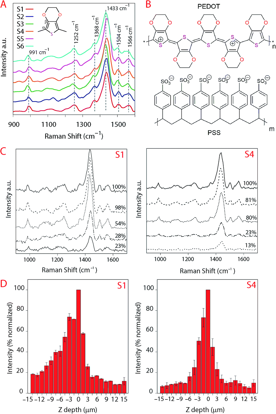 | ||
| Fig. 10 (A) Raman spectra of the printed PEDOT:PSS ink onto the substrates indicating the vibration frequency of the characteristic bands that is the symmetric stretch at 1433 cm−1 (CαCβ) and the asymmetric stretch (CC–O) at 1504 cm−1. These curves have been normalized at the 991 cm−1 band. (B) Chemical structure of PEDOT:PSS. (C) Raman YZ laser penetration analyses for S1 and S4 indicating the 5 spectra with the highest intensity from the focus point. This curves were not normalized. (D) Raman YZ profile of printed PEDOT:PSS ink ranging from 15 μm above and below the focus point. The negative values indicate the position in the YZ direction above the focus, zero indicates the position of the focus point and the positive ones below focus. We evaluated the band at 1504 cm−1 and the area within the frequency 1379–1482 cm−1 corresponding to the width of this band. | ||
In Fig. 10A the spectra of the printed PEDOT:PSS ink on each substrate are illustrated. Note that the curves in Fig. 10A were normalized to the highest intensity of the oxyethylene ring deformation band at the vibration frequency 991 cm−1, and all spectra were smoothed at 1 degree. The other vibration modes observed were at the highest intensity band at the frequency 1433 cm−1 and correspond to symmetric stretching (CαCβ), asymmetric stretching (CC–O) at 1504 cm−1, Cβ–Cβ stretching at 1368 cm−1 and asymmetric inter-ring stretching (Cα–Cα)59 at 1252 cm−1 indicating that there was no change in the structure of PEDOT in the ink/substrate interface. Due to the fluorescence during measurement of the substrate using Raman we also present the spectra acquired using FTIR in Fig. 9.
When the laser is distant from the focus point, a larger area will be excited by the laser beam which will impact the measurement because the signal being measured will account for the gains of a larger illuminated volume and the losses due to the surface not being in focus.60 It is the optical system that will dictate how much of the signal that is not in focus will be detected.
In Fig. 10C, the position of the laser was set to be 30 μm above and below the focus point and we plotted the data for the 5 spectra at the maximum intensities below the focus point. The loss of intensity of the laser is expressed in percentage of the signal compared to the maximum measured intensity. The maximum intensity that we evaluated was for the band correspondent to the asymmetric stretching (CC–O) at 1504 cm−1 and the area within the frequency 1379–1482 cm−1 corresponding to the width of this band. The software from the instrument consider the data above the focus point negative values, these measurements are equivalent to the laser moving away from the sample. Analogous to that, the positive data would be the data below the focus point, the measurement into the sample in depth (YZ-direction). This loss in intensity could also be due to the differences in refractive index, the reduction of the ink volume and etc. Our aim is to evaluate if there would be a change in the spectra in YZ direction characterizing chemical reactions but we did not observe changes in the spectra besides the loss of intensity meaning that the substrates remain inert when the ink penetrate the IRLs of the substrates.
The results show a higher intensity of the signal for the ink above the surface of S1 even at lower laser intensities (more distant from the surface) which we attribute to the ink density on top of the substrate for S1 being higher compared to the other substrates. That may also explain the lower electronic resistance measured for this substrate.
Noticing that the ink density could be evaluated using Raman, we obtained surface mapping of the printed surface in the XYZ direction to evaluate the ink distribution on the substrates in XY direction. The de-wetting of the ink through the intensity of the Raman signal was also evaluated. The analyses were done with an increment of 1.5 μm in a 500 μm2 area (see Fig. 11). For the XY mapping, the image at the highest Raman intensity was selected as representative of the mapping at the focus point. The measurement was done in all directions XYZ with the increment equal to 1.5 μm. 4 data points in Z-direction were set to precisely reach the data at the highest intensity and then collected the mapping data in XY direction at that Z position. The spectra were baseline corrected, and cosmic rays were removed. Red areas indicated stronger signals. Blue indicated no or negligible signal. The mapping can be compared with microscopy images of the same area in the same magnitude if we observe Fig. 12A for S1 and S3 we can make some correlations to the Raman mapping images, the image for S4 would be very similar to S3 (the other microscopy images are presented in the ESI Fig. S3†). Note that Fig. 11 does not present the printed lines in the printing direction as is the case in Fig. 12A. Please look at Fig. 11 in a vertical position for this comparison.
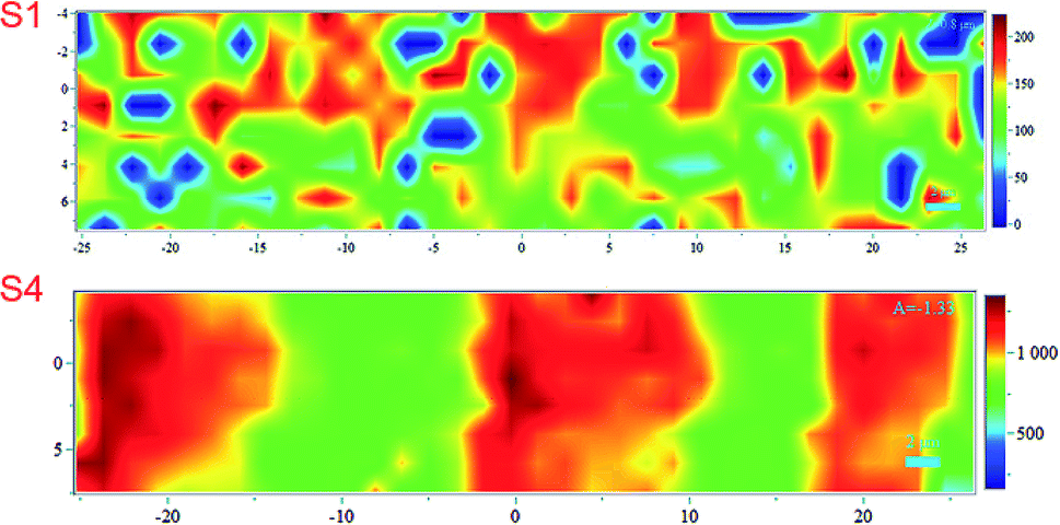 | ||
| Fig. 11 Raman mapping of the printed surface of S1 and S4 substrates. The scale bar indicates the maximum and minimum intensities for the band at 1504 cm−1. | ||
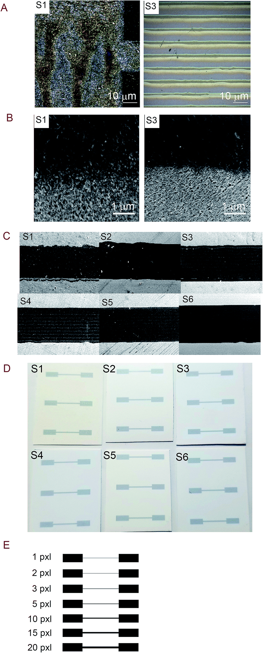 | ||
| Fig. 12 (A) To the left, Raman microscopy images (5× magnification) of the printed surfaces of S1 and to the right, the printed surface of S3 (10× magnification). (B) SEM images of the printed surfaces at the interface ink/substrate for substrates S1 and S3. Scale bar indicates 1 μm. (C) Magnified SEM images of the printed surfaces of a 20 pxl line with adjusted contrast. (D) Photograph of printed samples of 20 pxl lines (9 mm length) and contacts (4 mm length). (E) Template of the printed lines showing the line width in pixels to the left. | ||
We observe areas with print roughness especially pronounced for S1 and sharp lines with slightly uneven ink distribution for S3. In Fig. 12B some pigments in the CL1 of S1 are not fully covered with one printing layer (PL) of the ink as they are for S3 for example this create an uneven distribution of the ink that we also observed in the surface mapping (i.e., Fig. 11). In Fig. 11 the anisotropic ink distribution between S1 and S4 are evident. We performed profilometry on a 20 pxl printed line on S3, these results are presented in the ESI Fig. S6.†
The line quality of the printouts can be qualitatively evaluated from sections of the printed lines accessed by SEM illustrated in Fig. 12C. To the naked eye, the differences in printability are not evident as can be seen from the photographs of the print-outs in Fig. 12D. S1 present worse printing quality than the other substrates. With this, we would like to point out that a somewhat lower printing quality could be acceptable in exchange for better electronic properties and more sustainable substrates for printed electronics.
Although not in the scope of this study, authors have reported the modification of the surface of cellulose based substrates with hydrocarbons and fluorocarbon based resins that resulted in better electronic performance together with an improve in print resolution38–40,61 and in this way circumvent the high absorbency of the substrates that resulted in poor printability.
Part 3: electrical properties and applications
The electrical resistance was measured for the printed lines ranging from 1 to 20 pxl, the thickness of this substrates is presented in Table 5. The template illustrated in Fig. 12E was used to print the patterns in a number of different substrates to evaluate the influence of the line thickness. In Table 5, we present the measured values of the line width of the 20 pxl printed lines estimated using the SEM measurement tool.| Substrate | Width [μm] |
|---|---|
| S1 | 418.7 ± 21.7 |
| S2 | 447.8 ± 3.9 |
| S3 | 450.5 ± 5.8 |
| S4 | 437.3 ± 7.8 |
| S5 | 451.7 ± 5.7 |
| S6 | 468.8 ± 5.0 |
Differently than reported in the literature for silver nanoparticles inks62 which showed higher resistance for silica containing coated substrates, we did not observe a significant influence of the coating composition on the electrical properties of the printed lines using the PEDOT:PSS ink. As from our results, the substrates were chemically inert to the ink.
The impact on the electrical properties of the number of printing passes and the sintering was also evaluated. Considering the 20 pxl lines (see Fig. 13A), we measured a 400-fold lower resistance than for a 1 pxl width line printed with 1 PL (e.g., 0.11 MΩ and 38 MΩ respectively). Increasing the number of PLs reduce the resistance as can be seen from Fig. 13B and C. Comparing with the other substrates, the 20 pxl line printed in S1 show 100 fold lower resistance compared to the others (i.e, 0.11 MΩ for S1 and ≈13 MΩ for the other substrates with 1 PL). We attribute this to the higher roughness of substrate S1 (i.e., 105 nm) compared to the other substrates (≈10 nm) which creates areas of different ink density.
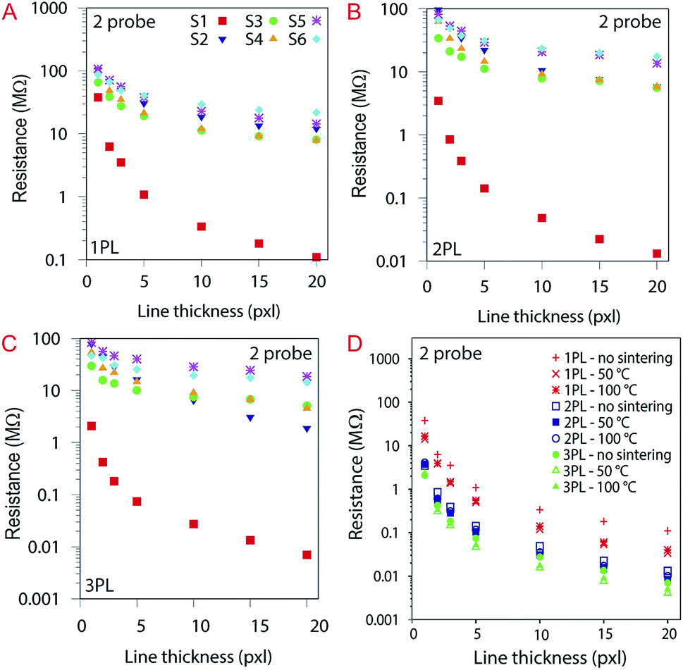 | ||
| Fig. 13 (A), (B) and (C) Resistance of the printed lines from 1, 2, 3, 5, 10, 15 and 20 pxl width with 1, 2 and 3 PLs, respectively, without sintering, indicating the drop in resistance for the lines printed in S1. (D) The influence of sintering temperature in resistance for S1. For better understanding, the data here are divided into three groups i.e., red (1 PL), green (2 PL) and blue (3 PL). | ||
The substrates were sintered for 30 minutes at 50 °C and 100 °C for each printed line illustrated in Fig. 13D, varying the number of PLs. The influence of sintering temperature in resistance for S1: the higher the number of PL, the lower the resistance. For better understanding, the data here are divided into three groups (i.e., red (1 PL), green (2 PL) and blue (3 PL)). Sintering did not affect significantly the resistance for the other substrates (see ESI Fig. S4†).
The sheet resistance of the printed lines were evaluated using a 4-probe measurement setup. The contact resistance is attenuated with this measurement setup therefore the values measured for resistance are much lower. S1 still show a lower resistance compared to the other substrates with values around 59 ± 0.2 kΩ sq−1 compared to an average of 550 kΩ sq−1 for the other substrates. Substrate S2 and S5 that contain a CL of AlO(OH) show slightly higher resistance than the other resin-coated substrates. These results are illustrated in Fig. 14.
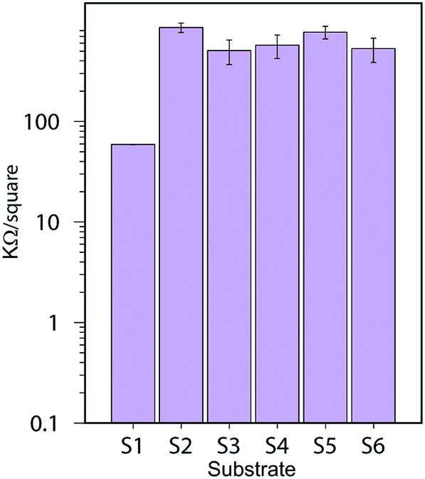 | ||
| Fig. 14 Sheet resistance of a 20 pxl printed line printed on the substrates S1 to S6. | ||
Conclusions
A paper substrate without a PE surface layer showed comparably low electrical/resistance for printed PEDOT:PSS lines despite a RMS surface roughness of 105 nm. The lack of the PE layer means that such water-based ink/substrate combinations could be recyclable. For all low roughness substrates investigated, pore size and surface energy were important characteristics. They influence de-wetting phenomena, and the final ink distribution. The Raman spectroscopy methodology was particularly successful in correlating ink distribution with printed line resistance.Conflicts of interest
The authors declare no conflict of interest.Acknowledgements
The Knowledge Foundation is acknowledged for funding. Viviane Forsberg also acknowledges ÅForsk Foundation (grant no. 18-281), J. Gust. Richert Foundation (grant no. 2018-00459), the Knut and Alice Wallenberg Foundation through the Wallenberg Wood Science Center and the Swedish Graphic Companies Federation for funding. The authors also acknowledge Ophelie Lancry (Horiba Scientific) and Magnus Hummelgård (Mid Sweden University) for valuable discussions about Raman spectroscopy and energy dispersive X-ray spectroscopy respectively. Vinay Kumar, Rajesh Koppolu and Martti Toivakka from Åbo Akademi are acknowledged for supplying the substrate S1. Henrik Andersson (Mid Sweden University) is acknowledged for supplying the substrates S2–S6 and for discussions about the inkjet printing part of this work. Tian Carey from Cambridge University is gratefully acknowledged for valuable contribution. Prof. Lars A. Berglund at KTH Royal Institute of Technology, Stockholm is gratefully acknowledged for fruitful discussions. Pavol Suly from Tomas Bata University is gratefully acknowledged for the help during the printing of the graphene lines presented in the ESI. This research has been supported by Treesearch.se.References
- H. Shirakawa, E. J. Louis, A. G. MacDiarmid, C. K. Chiang and A. J. Heeger, J. Chem. Soc., Chem. Commun., 1977, 578–580 RSC.
- A. G. MacDiarmid, Angew. Chem., Int. Ed., 2001, 40, 2581–2590 CrossRef CAS.
- H. Shirakawa, A. McDiarmid and A. Heeger, Chem. Commun., 2003, 2003, 1–4 RSC.
- C. Wang, H. Dong, W. Hu, Y. Liu and D. Zhu, Chem. Rev., 2012, 112, 2208–2267 CrossRef CAS PubMed.
- M. Nikolka and H. Sirringhaus, in Conjugated Polymer-Based OFET Devices, ed. J. R. Reynolds, B. C. Thompso and T. A. Skotheim, CRC Press, 2019, ch. Conjugated Polymers: Properties, Processing, and Applications Search PubMed.
- F. Jonas, W. Krafft and B. Muys, Macromolecular Symposia, 1995, pp. 169–173 Search PubMed.
- L. Groenendaal, F. Jonas, D. Freitag, H. Pielartzik and J. R. Reynolds, Adv. Mater., 2000, 12, 481–494 CrossRef CAS.
- N. Kim, I. Petsagkourakis, S. Chen, M. Berggren, X. Crispin, M. P. Jonsson and I. Zozoulenko, in Electric Transport Properties in PEDOT Thin Film, ed. J. R. Reynolds, B. C. Thompso and T. A. Skotheim, CRC Press, 2019, ch. Conjugated Polymers: Properties, Processing, and Applications Search PubMed.
- M. Berggren and G. G. Malliaras, Science, 2019, 364, 233–234 Search PubMed.
- B. Winther-Jensen and K. West, Macromolecules, 2004, 37, 4538–4543 CrossRef CAS.
- H. Sirringhaus, T. Kawase, R. H. Friend, T. Shimoda, M. Inbasekaran, W. Wu and E. P. Woo, Science, 2000, 290, 2123–2126 CrossRef CAS PubMed.
- T. Carey, S. Cacovich, G. Divitini, J. Ren, A. Mansouri, J. M. Kim, C. Wang, C. Ducati, R. Sordan and F. Torrisi, Nat. Commun., 2017, 8, 1202 CrossRef PubMed.
- A. G. Kelly, T. Hallam, C. Backes, A. Harvey, A. S. Esmaeily, I. Godwin, J. Coelho, V. Nicolosi, J. Lauth and A. Kulkarni, et al., Science, 2017, 356, 69–73 CrossRef CAS PubMed.
- F. Torrisi and T. Carey, Nano Today, 2018, 23, 73–96 CrossRef CAS.
- Y. H. Kim, C. Sachse, M. L. Machala, C. May, L. Müller-Meskamp and K. Leo, Adv. Funct. Mater., 2011, 21, 1076–1081 CrossRef CAS.
- L. Li, Y. Yu, G. J. Ye, Q. Ge, X. Ou, H. Wu, D. Feng, X. H. Chen and Y. Zhang, Nat. Nanotechnol., 2014, 9, 372 CrossRef CAS PubMed.
- M. Naguib, V. N. Mochalin, M. W. Barsoum and Y. Gogotsi, Adv. Mater., 2014, 26, 992–1005 CrossRef CAS PubMed.
- L. Niu, J. N. Coleman, H. Zhang, H. Shin, M. Chhowalla and Z. Zheng, Small, 2016, 12, 272–293 CrossRef CAS PubMed.
- S. Kim, A. Konar, W.-S. Hwang, J. H. Lee, J. Lee, J. Yang, C. Jung, H. Kim, J.-B. Yoo and J.-Y. Choi, et al., Nat. Commun., 2012, 3, 1011 CrossRef PubMed.
- V. Forsberg, R. Zhang, J. Bäckström, C. Dahlström, B. Andres, M. Norgren, M. Andersson, M. Hummelgård and H. Olin, PLoS One, 2016, 11, e0154522 CrossRef PubMed.
- Q. H. Wang, K. Kalantar-Zadeh, A. Kis, J. N. Coleman and M. S. Strano, Nat. Nanotechnol., 2012, 7(11), 699–712 CrossRef CAS PubMed.
- Y. Deng, Z. Luo, N. J. Conrad, H. Liu, Y. Gong, S. Najmaei, P. M. Ajayan, J. Lou, X. Xu and P. D. Ye, ACS Nano, 2014, 8, 8292–8299 CrossRef CAS PubMed.
- P. N. Nirmalraj, T. Lutz, S. Kumar, G. S. Duesberg and J. J. Boland, Nano Lett., 2011, 11, 16–22 CrossRef CAS PubMed.
- B. J. Worfolk, S. C. Andrews, S. Park, J. Reinspach, N. Liu, M. F. Toney, S. C. B. Mannsfeld and Z. Bao, Proc. Natl. Acad. Sci. U. S. A., 2015, 112, 14138–14143 CrossRef CAS PubMed.
- V. R. Feig, H. Tran and Z. Bao, ACS Cent. Sci., 2018, 4, 337–348 CrossRef CAS PubMed.
- H. Andersson, P. Šuly, G. Thungström, M. Engholm, R. Zhang, J. Mašlík and H. Olin, Journal of Low Power Electronics and Applications, 2019, 9, 14 CrossRef.
- W. Colglazier, Science, 2015, 349, 1048–1050 CrossRef CAS PubMed.
- M. Irimia-Vladu, Chem. Soc. Rev., 2014, 43, 588–610 RSC.
- T. Mori and S. Priya, MRS Bull., 2018, 43, 176–180 CrossRef.
- R. Martins, D. Gaspar, M. J. Mendes, L. Pereira, J. Martins, P. Bahubalindruni, P. Barquinha and E. Fortunato, Appl. Mater. Today, 2018, 12, 402–414 CrossRef.
- P. Ihalainen, A. Määttänen, J. Järnström, D. Tobjörk, R. Österbacka and J. Peltonen, Ind. Eng. Chem. Res., 2012, 51, 6025–6036 CrossRef CAS.
- D. E. Bugner, in Handbook of imaging materials, ed. A. S. Diamond and D. S. Weiss, Marcel Dekker, 2nd edn, 2002, ch. Paper and films for ink jet printing, pp. 603–627 Search PubMed.
- J. Kettle, T. Lamminmäki and P. Gane, Surf. Coat. Technol., 2010, 204, 2103–2109 CrossRef CAS.
- J. Schoelkopf, C. J. Ridgway, P. A. Gane, G. P. Matthews and D. C. Spielmann, J. Colloid Interface Sci., 2000, 227, 119–131 CrossRef CAS PubMed.
- C. J. Ridgway and P. A. Gane, Nord. Pulp Pap. Res. J., 2002, 17, 119–129 CAS.
- P. Samyn, J. V. Erps, H. Thienpont and G. Schoukens, Appl. Surf. Sci., 2011, 257, 5613–5625 CrossRef CAS.
- J. Wang, Z. Zheng, H. Li, W. Huck and H. Sirringhaus, Nat. Mater., 2004, 3, 171 CrossRef CAS PubMed.
- Z. Gozutok, O. Kinj, I. Torun, A. T. Ozdemir and M. S. Onses, Cellulose, 2019, 26, 3503–3512 CrossRef CAS.
- J. Lessing, A. C. Glavan, S. B. Walker, C. Keplinger, J. A. Lewis and G. M. Whitesides, Adv. Mater., 2014, 26, 4677–4682 CrossRef CAS PubMed.
- A. C. Glavan, R. V. Martinez, A. B. Subramaniam, H. J. Yoon, R. M. D. Nunes, H. Lange, M. M. Thuo and G. M. Whitesides, Adv. Funct. Mater., 2014, 24, 60–70 CrossRef CAS.
- S. Shen, W. K. Ng, L. S. O. Chia, Y. Dong and R. B. H. Tan, Cryst. Growth Des., 2012, 12, 4987–4994 CrossRef CAS.
- S. Ram, Infrared Phys. Technol., 2001, 42, 547–560 CrossRef CAS.
- P. Larkin, Infrared and Raman spectroscopy: principles and spectral interpretation, Elsevier, 2017 Search PubMed.
- B. Shokri, M. A. Firouzjah and S. Hosseini, Proceedings of 19th International Symposium on Plasma Chemistry Society, Bochum, Germany, 2009 Search PubMed.
- D. Wood and E. M. Rabinovich, Appl. Spectrosc., 1989, 43, 263–267 CrossRef CAS.
- G. L. Re, F. Lopresti, G. Petrucci and R. Scaffaro, Micron, 2015, 76, 37–45 CrossRef PubMed.
- K. Holmberg, B. Jönsson, B. Kronberg and B. Lindman, Surfactants and polymers in aqueous solution, Wiley, 2003 Search PubMed.
- A. Hamraoui and T. Nylander, J. Colloid Interface Sci., 2002, 250, 415–421 CrossRef CAS PubMed.
- P. A. Gane, J. P. Kettle, G. P. Matthews and C. J. Ridgway, Ind. Eng. Chem. Res., 1996, 35, 1753–1764 CrossRef CAS.
- C. J. Ridgway, P. A. Gane and J. Schoelkopf, J. Colloid Interface Sci., 2002, 252, 373–382 CrossRef CAS PubMed.
- C. J. Ridgway and P. A. Gane, Colloids Surf., A, 2002, 206, 217–239 CrossRef CAS.
- C. J. Van Oss, M. K. Chaudhury and R. J. Good, Chem. Rev., 1988, 88, 927–941 CrossRef CAS.
- W. Wu, R. J. Giese and C. Van Oss, Langmuir, 1995, 11, 379–382 CrossRef CAS.
- H. Busscher, A. van Pelt, P. de Boer, H. de Jong and J. Arends, Colloids Surf., 1984, 9, 319–331 CrossRef CAS.
- R. Bollström, A. Määttänen, D. Tobjörk, P. Ihalainen, N. Kaihovirta, R. Österbacka, J. Peltonen and M. Toivakka, Org. Electron., 2009, 10, 1020–1023 CrossRef.
- A. Marmur, Langmuir, 2003, 19, 8343–8348 CrossRef CAS.
- A. Marmur, in The chemistry of inkjet inks, ed. S. Magdassi, World Scientific, 2010, ch. Equilibrium Wetting Fundamentals, pp. 43–53 Search PubMed.
- R. D. Deegan, O. Bakajin, T. F. Dupont, G. Huber, S. R. Nagel and T. A. Witten, Nature, 1997, 389, 827 CrossRef CAS.
- J. M. D'Arcy, M. F. El-Kady, P. P. Khine, L. Zhang, S. H. Lee, N. R. Davis, D. S. Liu, M. T. Yeung, S. Y. Kim, C. L. Turner, A. T. Lech, P. T. Hammond and R. B. Kaner, ACS Nano, 2014, 8, 1500–1510 CrossRef PubMed.
- F. Adar, Spectroscopy, 2010 Search PubMed.
- Z. Tang, H. Li, D. W. Hess and V. Breedveld, Cellulose, 2016, 23, 1401–1413 CrossRef CAS.
- H. Andersson, A. Manuilskiy, C. Lidenmark, J. Gao, T. Öhlund, S. Forsberg, J. Örtegren, W. Schmidt and H.-E. Nilsson, Nanotechnology, 2013, 24, 455203 CrossRef CAS PubMed.
- J. Mašlík, H. Andersson, V. Forsberg, M. Engholm, R. Zhang and H. Olin, J. Instrum., 2018, 13, C12010 CrossRef.
Footnote |
| † Electronic supplementary information (ESI) available. See DOI: 10.1039/c9ra03801a |
| This journal is © The Royal Society of Chemistry 2019 |