
 Open Access Article
 This Open Access Article is licensed under a Creative Commons Attribution-Non Commercial 3.0 Unported Licence
The deviations of evaporation modes in two different morphologies of 2D WS2 film
Yanlu Yuab,
Lan Meng *ab,
Wei Yanc,
Jingjing Fengab,
Heng Lide and
Xiaohong Yan*ab
*ab,
Wei Yanc,
Jingjing Fengab,
Heng Lide and
Xiaohong Yan*ab
aCollege of Electronic and Optical Engineering & College of Microelectronics, Nanjing University of Posts and Telecommunications, Nanjing 210023, China. E-mail: menglan@njupt.edu.cn; yanxh@njupt.edu.cn
bKey Laboratory of Radio Frequency and Micro-Nano Electronics of Jiangsu Province, Nanjing 210023, China
cNew Energy Technology Engineering Laboratory of Jiangsu Provence & School of Science, Nanjing University of Posts and Telecommunications (NUPT), Nanjing 210023, China
dJiujiang Resarch Institute of Xiamen University, Jiujiang 332000, China
eFujian Provincial Key Laboratory of Semiconductors and Applications, Collaborative Innovation Center for Optoelectronic Semiconductors and Efficient Devices, Department of Physics, Xiamen University, Xiamen 361005, China
First published on 27th August 2019
Abstract
Exploring the inverse process of materials growth, evaporation of atoms from the material, is a crucial method to investigate the physical properties of two dimensional (2D) nanomaterials. Here, the evaporation modes of two different morphologies of 2D WS2 film, stacked film and normal film, were investigated by thermal annealing. It is found that the atomic evaporation rate increases and the crystallinity deteriorates when annealing temperature rises. During the evaporation process, atom evaporation firstly starts from the boundaries and defects. The evaporation rate is proportional to the free energy of S and W atoms, and inversely proportional to the local S–W atomic concentration. There is a striking difference in the evaporation modes between stacked film and normal film; layer-by-layer peeling off the surface only appears in normal film. These results imply that the interlayer coupling strength of stacked film is greater than that of the normal film with uniform thickness.
1. Introduction
The discovery of graphene has spawned entirely new fields of research on two dimensional (2D) layered materials since 2004. However, the metallic properties of graphene with zero-bandgap limits its applications in electronic circuits and field-effect transistors.1,2 Over the past ten years, a large number of different 2D materials with novel properties have been explored. Among them, 2D transition metal dichalcogenides (TMDs) have attracted a lot of attention due to their interesting electrical, chemical and optical properties.3–6 This category of materials may span the full range of electronic behavior from metallic to semi-conductive and wide band-gap insulating properties.7,8 Extensive investigations show that 2D TMDs have revealed affluent properties, such as, valley polarization,9,10 quantum spin Hall effect,11,12 type-II Weyl semimetal,13,14 etc. Besides, the applications and the synthesis techniques of 2D TMDs have also been investigated extensively up to now.15–20 However, the inverse process of film growth by thermal annealing, evaporation of atoms from the film as grown, is scarcely discussed. As a conventional technology, thermal annealing can help us further study the physical properties of the 2D nanomaterials. Based on previous research, annealing can be used to investigate the interlayer forces,21 the thermal stability of grain boundaries,22 phase transformation,23,24 etc. The coupling behavior of heterojunctions could be modulated by low temperature annealing.25 Besides, films can be thinned down to desired thickness by thermal annealing.26 Also, by using techniques such as in situ Transmission Electron Microscopy (TEM)27,28 and Scanning Electron Microscopy (SEM),29 it is possible to directly observe changes in the atomic microstructure before and after annealing. Nevertheless, the thermal annealing research for 2D TMDs film grown by chemical vapor deposition (CVD) method, especially when the annealing temperature is close to the growth temperature has not been reported up to now.In this paper, the effects of four annealing parameters: the annealing temperature, the carrier gas flow rate, the sample positions on the substrate and the annealing time on the morphologies of 2D WS2 film were explicitly explored. Our results show that the atomic evaporation rate gradually increases and the crystallinity becomes worse and worse when annealing temperature rises. More importantly, both of the two morphologies film (stacked film and normal film) obtained by the CVD method are peeled from the boundaries and defects. The evaporation rate is proportional to the free energy of S and W atoms, and inversely proportional to the local S–W atomic concentration. However, layer-by-layer peeling off the surface only appears in normal film, which is similar with the stripping sequence of few-layers flakes obtained by mechanical exfoliation.26 This implies that the normal film of WS2 behave more like mechanically exfoliated film, whose interlayer coupling is van der Waals force. Whereas there may be a “pinning effect” at the center of stacked film, whose interlayer coupling strength is larger than that of normal film.
2. Experiment results and discussion
In this work, we synthesize 2D WS2 film on SiO2 (300 nm)/Si substrates using chemical vapor deposition (CVD) method (see the Methods section). As shown in Fig. 1(a), two different morphologies of 2D WS2: normal film with uniform thickness and stacked film with center region thicker can be obtained on one substrate. The samples as grown were annealed in Ar gas atmosphere for a certain time, as shown in the schematic of Fig. 1(b). After the annealing process finished, these samples were rapidly cooled down to room temperature by moving the furnace away. It can be clearly seen that the area of the film is significantly reduced after annealing by comparing the scanning electron microscopy (SEM) images (Fig. 1(a) and (c)) of WS2 film before and after annealing. Besides, there are some film with fewer layers may disappear after annealing. Meanwhile, an interesting phenomenon appeared, the remaining film is surrounded by a circle of granules, as shown in Fig. 1(d). According to the energy dispersive spectrometer (EDS), the mainly constituents of these granules are W atoms, which escaped from the 2D WS2 flakes to gather together. This may indicate that S atoms are prone to evaporate with relative to W atoms at the same condition.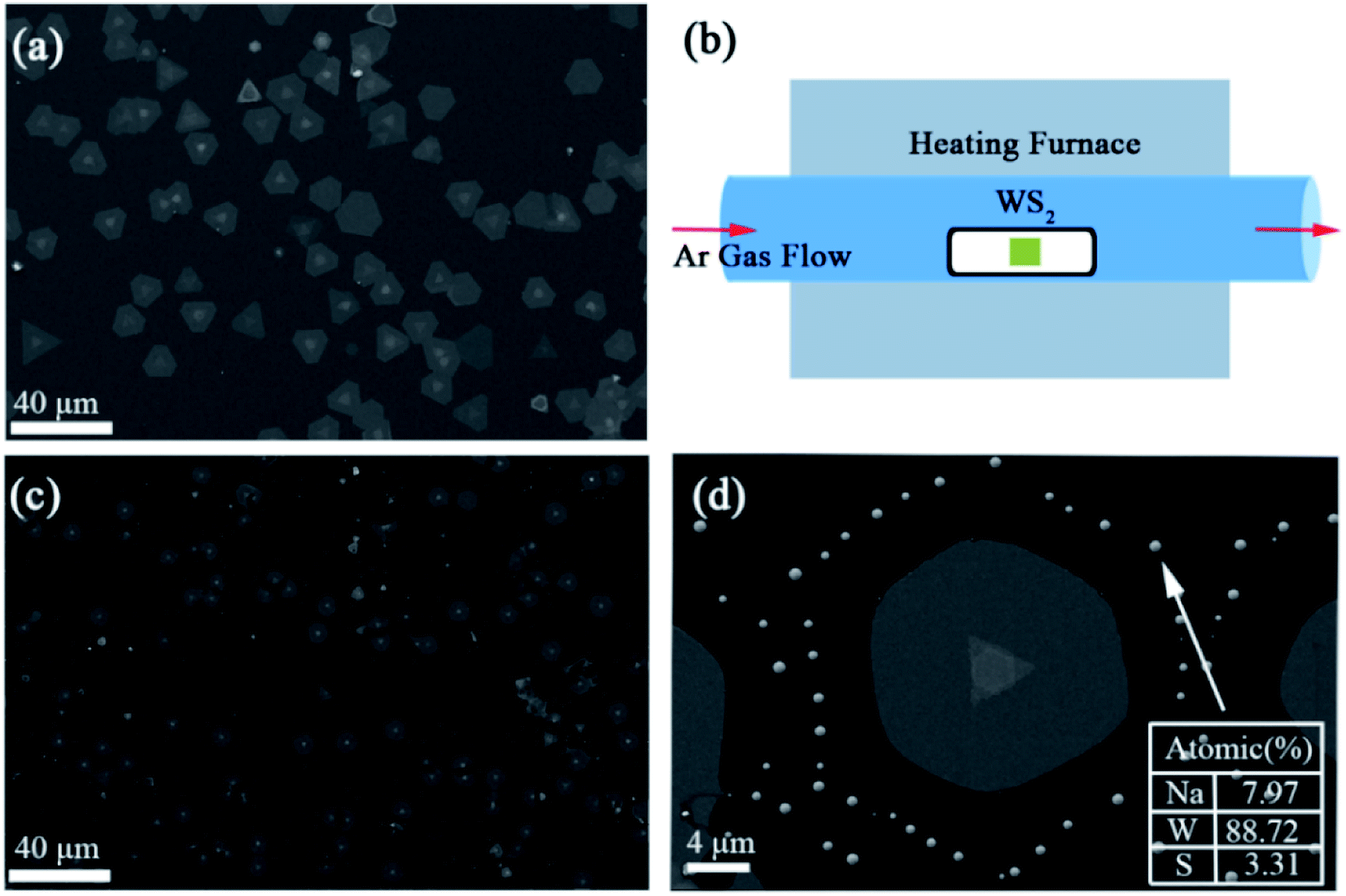 | ||
| Fig. 1 (a) and (c) SEM images of 2D WS2 film before and after annealing at 800 °C for 5 minutes (Ar gas flow rate ∼150 sccm). (b) Schematic of the thermal annealing for WS2 film. (d) is a high magnification SEM image of (c) with the EDS result of the granule. | ||
To further explore the mechanism of evaporation modes in 2D WS2 film with two different morphologies, annealing in different parameters were performed. Firstly, with other annealing parameters fixed (Ar gas flow rate ∼150 sccm, annealing time ∼3 min), we explore the influence of annealing temperature on the morphologies of WS2 flakes. Fig. 2 shows the optical micrographs of 2D WS2 film before and after annealing at 600 °C, 800 °C and 900 °C, respectively. It shows that there is a tiny decrease in the edge length of the triangular WS2 flake after annealing the samples at 800 °C by accurate measurement. While this phenomenon becomes extremely prominently when the annealing temperature increases to 900 °C. That is to say more atoms evaporate from the film in the same time when the annealing temperature increases. In other words, larger free energy of atoms will lead to a higher evaporation rate during annealing. To further obtain quantitative information about how the deviation of the evaporation rates depend on the different annealing temperature, Raman spectra were explored.
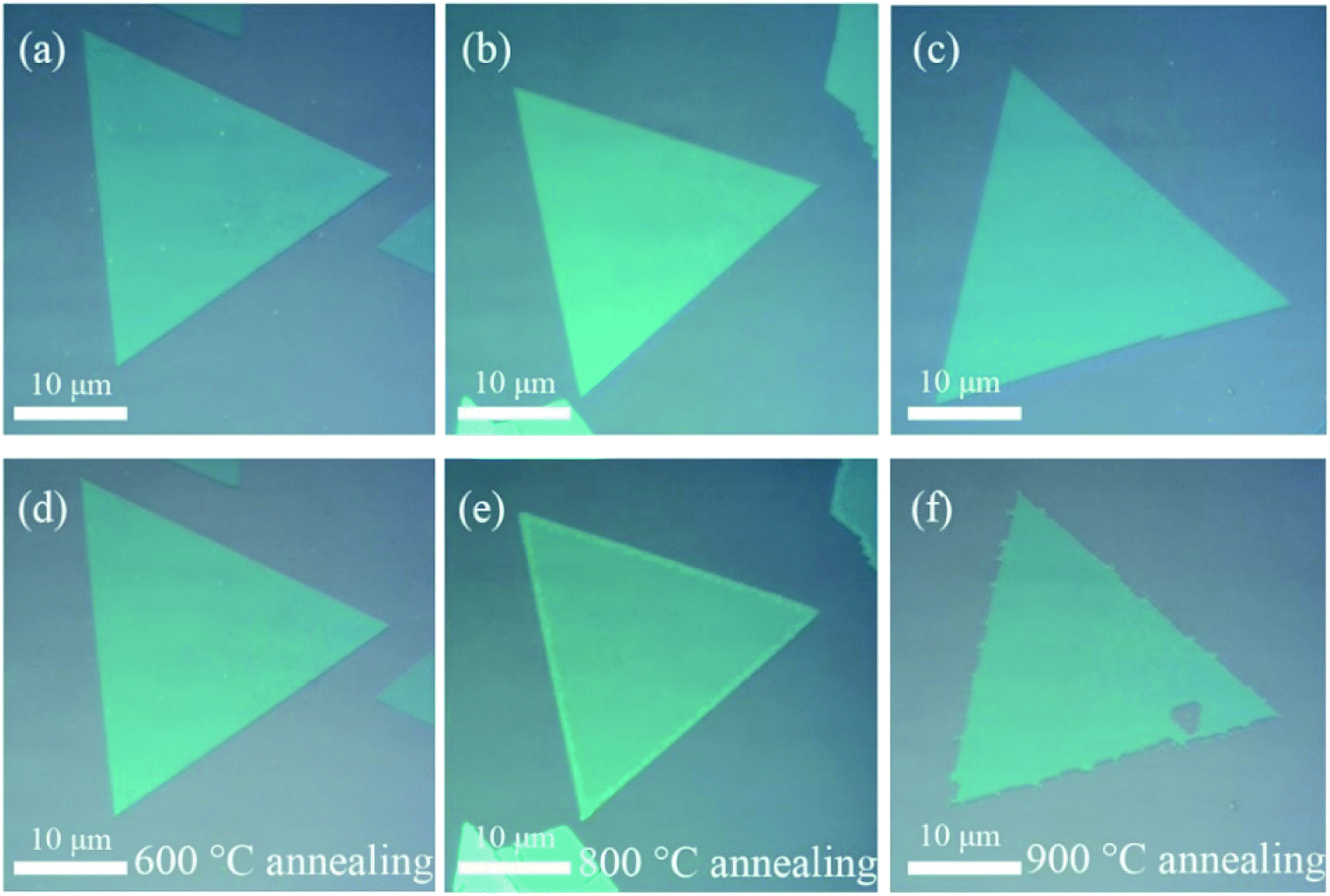 | ||
| Fig. 2 (a) and (d), (b) and (e), (c) and (f) are optical micrographs of WS2 film before and after annealing at 600 °C, 800 °C and 900 °C for 3 minutes, respectively (Ar gas flow rate ∼150 sccm). | ||
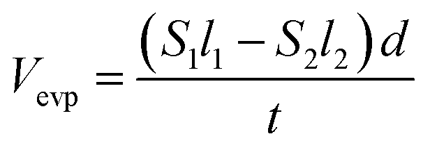
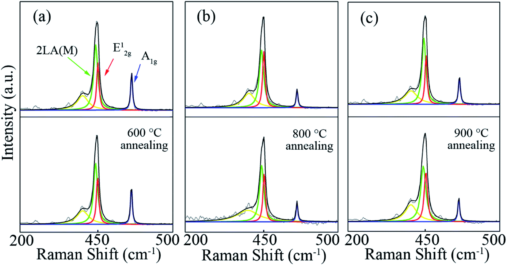
Fig. 3 shows the Raman spectra (excitation wavelength: 532 nm) performed on these triangular WS2 films in Fig. 2 before and after annealing. By fitting each Raman spectra with Lorentzian function, three Raman peaks: 2LA (M), E12g, and A1g are obtained. The statistical data of these Raman information are explicitly listed in the Table 1. By analyzing the Raman spectra, especially the relationship between the number of layers and A1g–E12g,30–32 the number of layers of the film could be determined. Here, the number of layers of the triangular flakes shown in Fig. 2 before annealing at 600 °C, 800 °C, and 900 °C are 2, 3, and 3, respectively, which change to 2, 3 and 2 after annealing. In other words, the number of layers of the film is reduced by one layer after annealing at 900 °C, but the film is only peeled off from the edge after annealing at 800 °C. Besides, by analyzing the optical micrographs through image segmentation method,33 the area of these films before and after annealing could be acquired. Therefore, the atomic evaporation rate of WS2 film at a certain annealing condition can be approximately estimated using this simple empirical formula:
 | ||
| Fig. 3 (a), (b) and (c) are Raman spectra of WS2 film before and after annealing at 600 °C, 800 °C and 900 °C, respectively (annealing time ∼3 minutes, Ar gas flow rate ∼150 sccm). | ||
| Annealing | E2g (cm−1) | A1g (cm−1) | A1g–E12g (cm−1) | FWHM of E12g (cm−1) | ΔFWHM (cm−1) | Area (×10−10 m2) | Atomic evaporation rate (min−1) | |
|---|---|---|---|---|---|---|---|---|
| 600 °C | Before | 354.3 | 419.3 | 65.0 | 5.9 | 1.1 | 7.55 | ≈0 |
| After | 354.3 | 419.3 | 65.0 | 7.0 | 7.55 | |||
| 800 °C | Before | 352.9 | 419.4 | 66.5 | 7.1 | 1.5 | 10.35 | 1.03 × 10⁵ |
| After | 352.9 | 419.4 | 66.5 | 8.6 | 9.63 | |||
| 900 °C | Before | 354.3 | 420.8 | 66.5 | 7.1 | 2.5 | 13.58 | 8.23 × 10⁵ |
| After | 354.3 | 419.3 | 65.0 | 9.6 | 7.85 |
Another important information can be achieved from the Raman spectra, that is full-width at half maximum (FWHM) of E12g, which reflects of the structural distribution of film.35 The higher the crystallinity, the narrower the FWHM of E12g. In Table 1, it can be clearly seen that the FWHM of E12g becomes larger after annealing, which demonstrates the crystallinity of the film deteriorated and more defect emerged after annealing. Furthermore, the variations of FWHM of E12g before and after annealing at 600 °C, 800 °C, and 900 °C are 1.1, 1.5 and 2.5, respectively. Therefore, we can draw a conclusion that the higher the annealing temperature, the atomic vibration becomes stronger and the crystallinity of the film is destroyed more severely. This can also be further confirmed by Fig. 2(f), where an observable vacancy emerges within the triangular film after annealing at 900 °C.
Carrier gas flow rate is another parameter which may exert significant influence on the evaporation of atoms during annealing process. Fig. 4(a)–(c) are optical micrographs before and after annealing 2D WS2 samples at 50 sccm and 300 sccm Ar gas flow rate (800 °C, annealing time ∼5 minutes), respectively. We observe that the evaporation rate of film increases remarkably as the carrier gas rate increases. Besides, we found that the evaporation rate of atoms during annealing is closely related to the position of the flakes on the substrate. As shown in Fig. 4(d)–(f), the remaining area of the film gradually increases along the direction of the Ar gas. Another interesting phenomenon is that the inner part of stacked film always stripped at the end during the annealing process, which is completely different from the stripping sequence of mechanical exfoliated layered film, with layer-by-layer peeling mode during the annealing process.
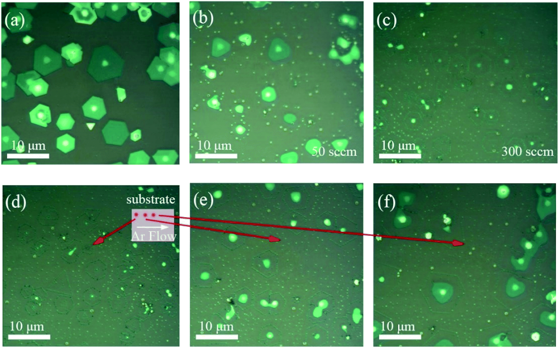 | ||
| Fig. 4 (a) Optical micrographs of 2D WS2 before annealing. (b) and (c) Optical micrographs of film annealing at 50 sccm and 300 sccm of carrier gas flow rate, respectively (annealing temperature ∼800 °C, annealing time ∼5 min). (d)–(f) Optical micrographs of different locations along the direction of carrier gas at the same sample (annealing temperature ∼800 °C, annealing time ∼5 min, carrier gas flow rate ∼300 sccm). | ||
In fact, carrier gas flow rate and the position of the flakes on the substrate exert similar effect on the evaporation rate during the annealing process. The evaporated S and W atoms are continuously transported backward by the carrier gas, and the delivery rate is proportional to the rate of the carrier gas. Therefore, higher carrier gas rate would result in lower remainder local S–W atomic concentration evaporated from WS2 film. Oppositely, the carrier gas will increase the local S–W atomic concentration at downstream part. Based on the above discussion, it can be concluded that evaporation rate is negatively correlated with the “local S–W atomic concentration”.
Another critical factor affecting the morphology of 2D WS2 film is annealing time. As it is difficult to observe the variations of 2D WS2 film in real-time during annealing process, we conduct short-time and continuously annealing one substrate to simulate continuous changes. Fig. 5(a)–(h) show the morphologies of 2D WS2 film under series of annealing for 0, 2, 4, 6, 8, 11, 14, 17 minutes, respectively. In addition to the decreased area of flakes as mentioned above, which means atoms gradually evaporate from the boundaries, vacancies in many flakes are also observed during annealing process.
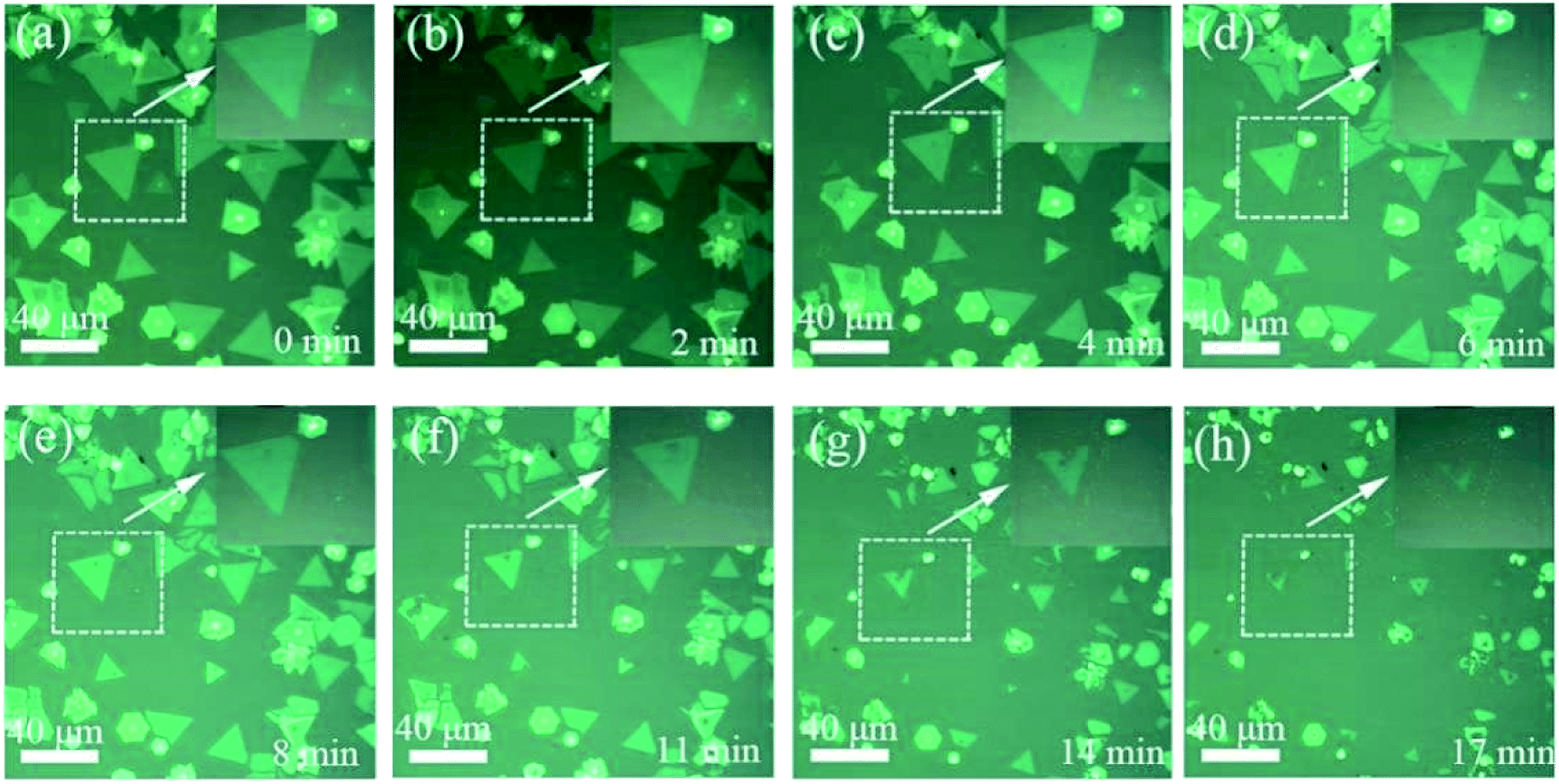 | ||
| Fig. 5 Optical micrographs of 2D WS2 film annealing for 0, 2, 4, 6, 8, 11, 14, 17 minutes (annealing temperature ∼800 °C, Ar gas flow rate ∼150 sccm), respectively. | ||
Like the mechanically exfoliated film,16,36 defects are ubiquitous among the films obtained by CVD method,37,38 atoms near the defects are more unstable, so these atoms are prone to evaporate firstly during the high temperature annealing process. As a result, defects will gradually expand to become vacancies and new boundaries, as shown in Fig. 5(d)–(h). Therefore, our experimental results demonstrate that atoms evaporation firstly starts from the boundaries and defects during the annealing process.
In order to further explore the influence of annealing on the morphologies of 2D WS2 film, atomic force microscopy (AFM) was employed to measure the thickness variation of WS2 flakes in our experiments. Fig. 6(a), (b), (e) and (f) show the variation of morphologies of normal WS2 film and stacked WS2 film before and after annealing. In our experiments, the distance between these two flakes on the substrate does not exceed 100 μm, so it's convinced that the four annealing parameters we have mentioned above are identical. As can be seen from Fig. 6(b) and (f), vacancies emerge on both types of WS2 film after annealing, which are marked by the red arrows. More importantly, from the deviation of height profiles between normal film and stacked film in Fig. 6(c) and (g), we can clearly find that the stacked film peeled only from the edges, but the normal film peeled not only from the edges but also peeled layer-by-layer from the surface. This means the evaporation rate of uppermost layer for stacked film is much lower than that of the boundaries. Furthermore, friction force microscope (FFM) measurements, shown in Fig. 6(d) and (h), demonstrate that the friction of both kinds of film increase after annealing. This further reveal that the roughness of WS2 film increase, and further demonstrate the increased defects or vacancies after annealing.
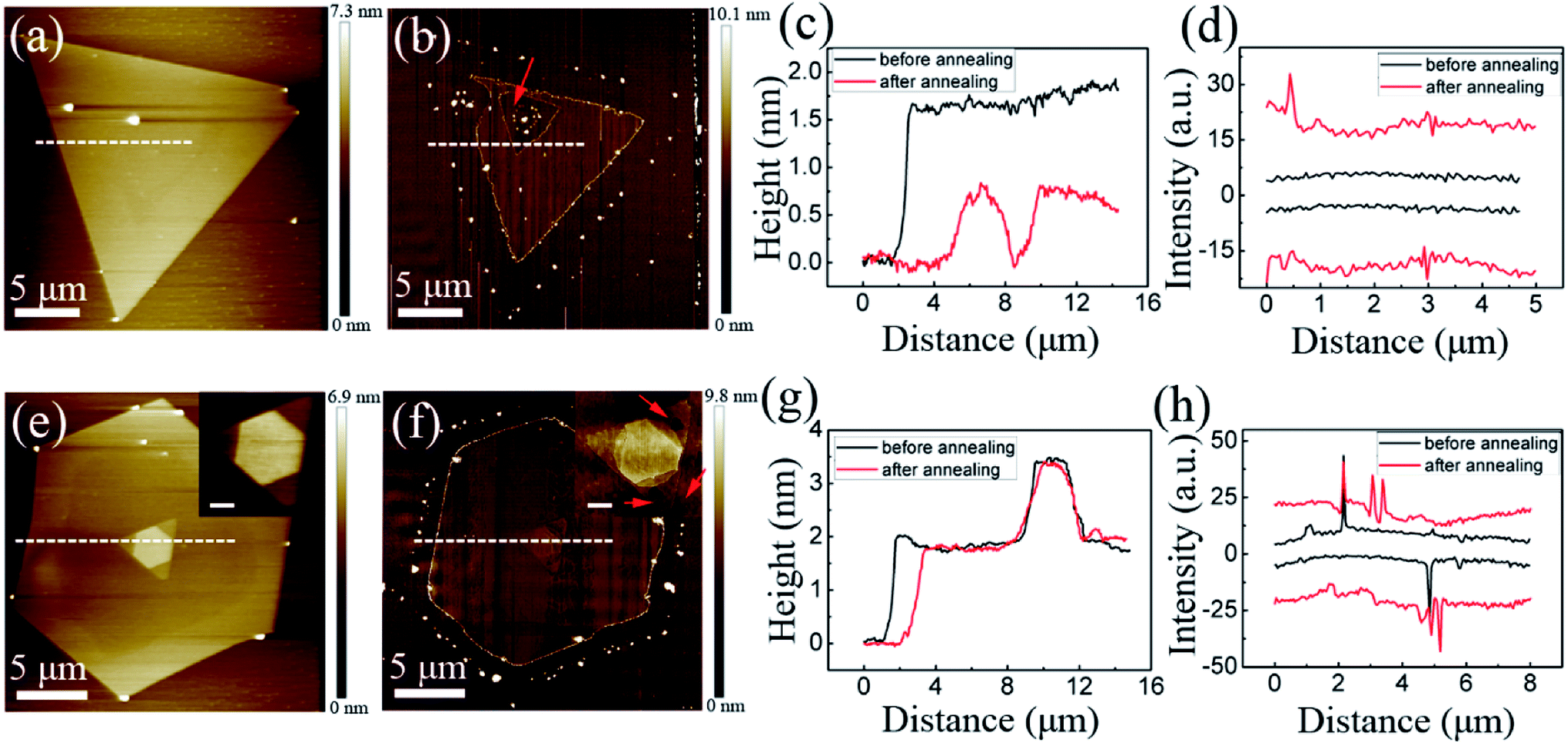 | ||
| Fig. 6 (a) and (b) AFM images of normal WS2 film before and after annealing (annealing temperature ∼800 °C, annealing time ∼10 minutes, Ar gas flow rate ∼150 sccm). (e) and (f) AFM images of stacked WS2 film before and after annealing, the scale bar in the insets in (e) and (f) is 1 μm. (c) and (g) Cross-sectional profiles correspond to the dotted lines in (a), (b), (e) and (f), respectively. (d) and (h) Friction curves obtained on the surface of 2D WS2 before and after annealing. | ||
Up to now, it is most fascinating to us: what is the origin of the deviation of evaporation modes between normal WS2 film and stacked WS2 film. As the evaporation mode of normal WS2 film with layer-by-layer peeled from the surface is much analogous to that of mechanically exfoliated film. So, the inner structure and interlayer coupling of normal WS2 film synthesized by CVD method and mechanically exfoliated 2D film are similar. As we know, the stronger binding force of one atom with the surrounding atoms, the more difficult for this atom to evaporate during annealing. Therefore, the stacked WS2 film synthesized by CVD method peeled only from the edge and defects, which may indicate that the interlayer coupling strength of stacked film is stronger than that of normal film and mechanically exfoliated film. Combining with the unique stacked pattern of these stacked film, we speculate that the much stronger interlayer coupling strength may come from the “pinning effect” at the central region of the stacked film.
This deviation of evaporation modes between normal and stacked film can be further confirmed by comparing the Raman spectra of WS2 film before and after annealing for a long time or higher temperature. As shown in Fig. 7(a), A, B1, B2 are Raman spectra for the normal film, outer region and center region of the stacked film before annealing, which are denoted by the blue arrows in the model diagram of Fig. 7(b) and (c). A′, B1′, B2′ are Raman spectra obtained on the same positions as A, B1, B2 after the sample was annealed at 800 °C for 10 minutes. By fitting each Raman spectra with Lorentzian function, it can be clearly seen that there is an obvious difference in the E12g peak before and after annealing, which represents the in-plane vibrations of W and S atoms.39,40 The strength of E12g peak of A and B1 spectra significantly reduce after annealing. This means that a large number of S–W bonds are destroyed during the annealing process,41 resulting in new defects, which is also consistent well with the friction measurements. However, the deviation of Raman spectra in the center part (B2) of stacked film before and after annealing could be ignored, which means the S–W bonds here are rarely destroyed. This result also confirms the “pinning effect” we mentioned above. According to the results and analysis above, we propose the diagram model illustrating the evaporation modes for normal 2D WS2 film and staked 2D film, as shown in Fig. 7(b) and (c). Further, we could deduce that the deviation of evaporation mode between stacked film and normal film may stem from their growth mechanism's disparity.
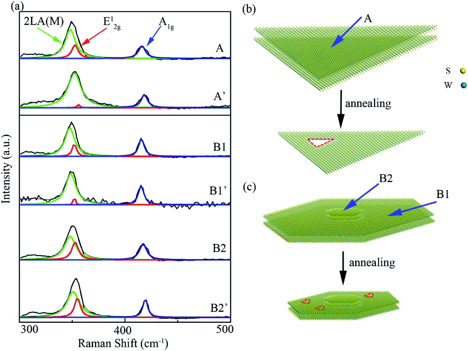 | ||
| Fig. 7 (a) A, B1, B2 are Raman spectra for the normal film, outer region and center region of the stacked film before annealing. A′, B1′, B2′ are Raman spectra obtained on the same position as A, B1, B2 after annealing (annealing temperature ∼800 °C, annealing time ∼10 minutes, Ar gas flow rate ∼150 sccm). (b) and (c) Diagram model illustrating the evaporation modes for normal 2D WS2 film and staked 2D film. | ||
3. Conclusion
In conclusion, we have studied the evaporation mode of two different morphologies of 2D WS2: normal film with uniform thickness and stacked film with center region thicker by thermal annealing. The evolution of morphologies in 2D WS2 film were explicitly explored by modulating four annealing parameters: the annealing temperature, the carrier gas flow rate, the position of the flakes on the substrate and the annealing time. The microstructure and quality of 2D WS2 were characterized by SEM, optical microscopy, AFM and Raman spectroscopy. The atomic evaporation rate of WS2 film at a certain annealing condition can be approximately estimated after recognizing the film area and layer numbers before and after annealing. We observe the evaporation rate is proportional to the free energy of S and W atoms, and inversely proportional to the local S–W atomic concentration. There is a striking difference in the evaporation mode between stacked film and normal film: stacked film peeled only from the boundaries and defects, but normal film peeled not only from the boundaries and defects but also peeled layer-by-layer from the surface. This implies that normal film of 2D WS2 behave more like mechanically exfoliated film, whose interlayer coupling is van der Waals force. Whereas there may be a “pinning effect” at the center of stacked film, whose interlayer coupling strength is larger than that of normal film.4. Methods
4.1 CVD synthesis of 2D WS2 film
The stacked film and normal film were grown by CVD method at atmospheric pressure with S and WO3 as precursors. Like the usual method, S powder (Alpha Aesar, 99.5%, 300 mg) and WO3 powder (Alpha Aesar, 99.5%, 30 mg) were placed in two furnaces (low temperature zone and high temperature zone) respectively, at the same time, SiO2 (300 nm)/Si substrates were placed in growth zone which was 2 cm away from the WO3. Before heating, the tube was pumped down to 20 Pa and flushed with 300 sccm high-purity Ar gas several times to exclude oxygen, then filled with Ar gas until the pressure in the tube is atmospheric pressure. Subsequently, Ar gas flow rate was adjusted to 120 sccm and kept until the end of the experiment. During the heating process, the low temperature zone for S precursors was first kept at room temperature for 24 minutes, then heated to 250 °C in 8 minutes, and held for 17 minutes. Meanwhile, the high temperature furnace for WO3 precursors and SiO2 (300 nm)/Si substrates were heated from room temperature to 1150 °C and 880 °C in 34 minutes, respectively, and then held for 15 minutes for growth. After growth process, the furnace was removed to allow the substrate naturally cooled.Conflicts of interest
We declare that we have no financial and personal relationships with other people or organizations that can inappropriately influence our work, there is no professional or other personal interest of any nature or kind in any product, service or company that could be construed as influencing the position presented in this manuscript submitted.Acknowledgements
This work was supported by the National Natural Science Foundation of China (11504180), the Natural Science Foundation of Jiangsu Province (BK20180740), Project funded by China Postdoctoral Science Foundation (BX20180145), NJUPTSF (NY218135), Fundamental Research Funds for the Central Universities (20720170084).References
- M. Sprinkle, D. Siegel, Y. Hu, J. Hicks, A. Tejeda, A. Taleb-Ibrahimi, P. Le Fevre, F. Bertran, S. Vizzini, H. Enriquez, S. Chiang, P. Soukiassian, C. Berger, W. A. de Heer, A. Lanzara and E. H. Conrad, Phys. Rev. Lett., 2009, 103, 226803 CrossRef CAS PubMed.
- M. Y. Han, B. Ozyilmaz, Y. Zhang and P. Kim, Phys. Rev. Lett., 2007, 98, 206805 CrossRef PubMed.
- S. Jeong-Gyu, P. Jusang, L. Wonseon, C. Taejin, J. Hanearl, L. C. Wan, H. Sung-Hwan, M. Jae Min, J. Jae-Hoon and K. Soo-Hyun, ACS Nano, 2013, 7, 11333–11340 CrossRef PubMed.
- K. Yu, S. Shogo, M. Shohei, H. Hiroki, L. Zheng, W. Kenji, T. Takashi, S. Kazu, M. Yutaka and M. Yasumitsu, ACS Nano, 2015, 9, 4056–4063 CrossRef PubMed.
- Z. Yu, Z. Yanfeng, J. Qingqing, J. Jing, Y. Hongtao, S. Jianping, G. Teng, M. Donglin, L. Mengxi and C. Yubin, ACS Nano, 2013, 7, 8963–8971 CrossRef PubMed.
- A. P. S. Gaur, S. Sahoo, J. F. Scott and R. S. Katiyar, J. Phys. Chem. C, 2015, 119, 5146–5151 CrossRef CAS.
- D. Lloyd, X. Liu, J. W. Christopher, L. Cantley, A. Wadehra, B. L. Kim, B. B. Goldberg, A. K. Swan and J. S. Bunch, Nano Lett., 2016, 16, 5836–5841 CrossRef CAS PubMed.
- Y. Guo, D. Sun, B. Ouyang, A. Raja, J. Song, T. F. Heinz and L. E. Brus, Nano Lett., 2015, 15, 5081–5088 CrossRef CAS PubMed.
- K. F. Mak, K. He, J. Shan and T. F. Heinz, Nat. Nanotechnol., 2012, 7, 494–498 CrossRef CAS PubMed.
- S. Wu, C. Huang, G. Aivazian, J. S. Ross, D. H. Cobden and X. Xu, ACS Nano, 2013, 7, 2768–2772 CrossRef CAS PubMed.
- M. A. Cazalilla, H. Ochoa and F. Guinea, Phys. Rev. Lett., 2014, 113, 077201 CrossRef CAS PubMed.
- W. Feng, Y. Yao, W. Zhu, J. Zhou, W. Yao and D. Xiao, Phys. Rev. B: Condens. Matter Mater. Phys., 2012, 86, 165108 CrossRef.
- H. Ma, P. Chen, B. Li, J. Li, R. Ai, Z. Zhang, G. Sun, K. Yao, Z. Lin, B. Zhao, R. Wu, X. Tang, X. Duan and X. Duan, Nano Lett., 2018, 18, 3523–3529 CrossRef CAS PubMed.
- S. Y. Chen, T. Goldstein, D. Venkataraman, A. Ramasubramaniam and J. Yan, Nano Lett., 2016, 16, 5852–5860 CrossRef CAS PubMed.
- Y. Gao, Z. Liu, D. M. Sun, L. Huang, L. P. Ma, L. C. Yin, T. Ma, Z. Zhang, X. L. Ma, L. M. Peng, H. M. Cheng and W. Ren, Nat. Commun., 2015, 6, 8569 CrossRef CAS PubMed.
- J. Wu, H. Li, Z. Yin, H. Li, J. Liu, X. Cao, Q. Zhang and H. Zhang, Small, 2013, 9, 3314–3319 CAS.
- S. Wang, Y. Rong, Y. Fan, M. Pacios, H. Bhaskaran, K. He and J. H. Warner, Chem. Mater., 2014, 26, 6371–6379 CrossRef CAS.
- A. Thangaraja, S. M. Shinde, G. Kalita and M. Tanemura, Mater. Lett., 2015, 156, 156–160 CrossRef CAS.
- J. Zhou, J. Lin, X. Huang, Y. Zhou, Y. Chen, J. Xia, H. Wang, Y. Xie, H. Yu, J. Lei, D. Wu, F. Liu, Q. Fu, Q. Zeng, C. H. Hsu, C. Yang, L. Lu, T. Yu, Z. Shen, H. Lin, B. I. Yakobson, Q. Liu, K. Suenaga, G. Liu and Z. Liu, Nature, 2018, 556, 355–359 CrossRef CAS PubMed.
- H. Song, X. Wang, M. Lan and X. Yan, Mater. Sci., 2017, 52, 7215–7223 CrossRef.
- W. Lu, Y. Zhang, Z. Zhu, J. Lai, C. Zhao, X. Liu, J. Liu and D. Sun, Nanotechnology, 2016, 27, 414006 CrossRef PubMed.
- S. Cai, W. Zhao, A. Zafar, Z. Wu, Y. Tao, K. Bi, Z. Wei, Z. Ni and Y. Chen, Mater. Res. Express, 2017, 4, 106202 CrossRef.
- Y. Yu, G. H. Nam, Q. He, X. J. Wu, K. Zhang, Z. Yang, J. Chen, Q. Ma, M. Zhao, Z. Liu, F. R. Ran, X. Wang, H. Li, X. Huang, B. Li, Q. Xiong, Q. Zhang, Z. Liu, L. Gu, Y. Du, W. Huang and H. Zhang, Nat. Chem., 2018, 10, 638–643 CrossRef CAS PubMed.
- H. Huang, Y. Cui, Q. Li, C. Dun, W. Zhou, W. Huang, L. Chen, C. A. Hewitt and D. L. Carroll, Nano Energy, 2016, 26, 172–179 CrossRef.
- F. Wang, J. Wang, S. Guo, J. Zhang, Z. Hu and J. Chu, Sci. Rep., 2017, 7, 44712 CrossRef CAS PubMed.
- X. Lu, M. I. Utama, J. Zhang, Y. Zhao and Q. Xiong, Nanoscale, 2013, 5, 8904–8908 RSC.
- F. Niekiel, S. M. Kraschewski, P. Schweizer, B. Butz and E. Spiecker, Acta Mater., 2016, 115, 230–241 CrossRef CAS.
- J. Kling, T. W. Hansen and J. B. Wagner, Carbon, 2016, 99, 261–266 CrossRef CAS.
- Z.-J. Wang, G. Weinberg, Q. Zhang, T. Lunkenbein, A. Klein-Hoffmann, M. Kurnatowska, M. Plodinec, Q. Li, L. Chi and R. Schloegl, ACS Nano, 2015, 9, 1506–1519 CrossRef CAS PubMed.
- H. R. Gutierrez, N. Perea-Lopez, A. L. Elias, A. Berkdemir, B. Wang, R. Lv, F. Lopez-Urias, V. H. Crespi, H. Terrones and M. Terrones, Nano Lett., 2013, 13, 3447–3454 CrossRef CAS PubMed.
- A. Berkdemir, H. R. Gutiérrez, A. R. Botello-Méndez, N. Perea-López, A. L. Elías, C.-I. Chia, B. Wang, V. H. Crespi, F. López-Urías, J.-C. Charlier, H. Terrones and M. Terrones, Sci. Rep., 2013, 3, 1755 CrossRef.
- W. Zhao, Z. Ghorannevis, K. K. Amara, J. R. Pang, M. Toh, X. Zhang, C. Kloc, P. H. Tan and G. Eda, Nanoscale, 2013, 5, 9677–9683 RSC.
- N. R. Pal and S. K. Pal, Pattern Recognit., 1993, 26, 1277–1294 CrossRef.
- L. Ma, Y. Tan, M. Ghorbani-Asl, R. Boettger, S. Kretschmer, S. Zhou, Z. Huang, A. V. Krasheninnikov and F. Chen, Nanoscale, 2017, 9, 11027–11034 RSC.
- A. McCreary, A. Berkdemir, J. Wang, M. A. Nguyen, A. L. Elías, N. Perea-López, K. Fujisawa, B. Kabius, V. Carozo, D. A. Cullen, T. E. Mallouk, J. Zhu and M. Terrones, Mater. Res., 2016, 31, 931–944 CrossRef CAS.
- P. Kumar, D. Chatterjee, T. Maeda, A. Roy, K. Kaneko and V. Balakrishnan, Nanoscale, 2018, 10, 16321–16331 RSC.
- Z. Liu, K. Suenaga, Z. Wang, Z. Shi, E. Okunishi and S. Iijima, Nat. Commun., 2011, 2, 213 CrossRef PubMed.
- H. Y. Jeong, Y. Jin, S. J. Yun, J. Zhao, J. Baik, D. H. Keum, H. S. Lee and Y. H. Lee, Adv. Mater., 2017, 29, 1605043 CrossRef PubMed.
- R. Saito, Y. Tatsumi, S. Huang, X. Ling and M. S. Dresselhaus, Phys. Condens. Matter, 2016, 28, 353002 CrossRef CAS PubMed.
- F. Liang, H. Xu, X. Wu, C. Wang, C. Luo and J. Zhang, Chin. Phys. B, 2018, 27, 037802 CrossRef.
- L. Su, Y. Yu, L. Cao and Y. Zhang, Nano Res., 2015, 8, 2686–2697 CrossRef CAS.
| This journal is © The Royal Society of Chemistry 2019 |