
 Open Access Article
 This Open Access Article is licensed under a
 Creative Commons Attribution 3.0 Unported Licence
A graphene/Si Schottky diode for the highly sensitive detection of protein
Ali Akbar Noroozi and
Yaser Abdi *
*
Nanophysics Research Laboratory, Department of Physics, University of Tehran, Tehran, Iran. E-mail: y.abdi@ut.ac.ir
First published on 24th June 2019
Abstract
Herein, a graphene/Si-based device was introduced for bovine serum albumin (BSA) sensing. In this study, it is shown that the Schottky junction at the interface of graphene/Si is highly sensitive to BSA under UV light exposure. The reverse bias current of the junction, which is sensitive to UV light, changes under exposure to BSA at different concentrations. By UV light absorption, we showed that the addition of the BSA solution to the junction affected the output characteristic of the fabricated device. Moreover, the output characteristic of the device shows that the device can be considered as a self-powered detector that would reduce the need for batteries. The results obtained in this study would open up a way towards the fabrication of an on-chip biosensor for the sensing of biological agents such as BSA.
1. Introduction
Graphene, a two-dimensional material, has been widely used for the fabrication of chemical sensors, photodetectors and biosensors.1–3 The extremely high surface-to-volume ratio makes graphene-based sensors highly sensitive to the changes in the chemical composition of an environment or biomass.4–7 Graphene has been used as a platform for the detection of different types of biomacromolecules such as DNA and proteins.8–11 Among biomacromolecules, serum albumin is the most abundant blood protein and essential for the growth of activated human lymphocytes.12 Consequently, the monitoring of serum albumin concentration would be useful. Because of its structural homology with human serum albumin, bovine serum albumin (BSA) is an appropriate protein to be used as a model protein for investigations and studies. The determination of serum albumin concentration is a critical part of protein studies. Therefore, some studies focusing on the quantification of the amount of protein present in a sample using efficient and low-cost methods have been reported.13,14 The common method for the determination of BSA concentration is based on the detection of UV absorbance of the samples. Most proteins exhibit a distinct ultraviolet light absorption maximum at 280 nm due to the presence of tyrosine and tryptophan. Since the tyrosine and tryptophan contents of various enzymes vary within narrow limits, the absorption peak at 280 nm has been used as a rapid and sensitive measure of protein concentration.15 In this method, the ratio of the absorbance at 280 nm for the target samples versus the absorbance of the sample at known concentration is measured. This method has moderate sensitivity with high material requirement. To reduce the material requirement and increase the sensitivity, it is necessary to focus on the on-chip measurements. In this study, we report the on-chip detection of BSA using a graphene/Si-based device.In recent years, the graphene/Si junction has been utilized for the fabrication of highly sensitive photodetectors with sensitivities as high as 1–10 A W−1.16–19 Due to its wide range of absorption, graphene/Si is a promising candidate for photo-detection from the UV to the IR range.20,21 Recently, we have reported the fabrication of highly sensitive broadband photodetectors based on the vertical Schottky junction of graphene/Si.22 On the other hand, graphene/Si-based diodes have been reported to be utilized for chemical and glucose sensing. Sakr et al. have utilized graphene-Schottky junction for non-enzymatic glucose sensing. Their sensor shows a linear response to glucose concentration in the range from 0 to 15 mmol L−1 with the detection limit of 0.5 mmol L−1.23 It has been shown that chemical adsorption on graphene sheets changes the electronic properties of graphene. Consequently, it is possible to modify the electrical characteristics of the graphene/Si junction via chemical adsorption. Based on this idea, Kim et al. have reported a graphene/Si-based diode sensor in which the chemical agent has been directly applied onto the graphene sheet using a pipette.24
In this study, we report the fabrication of a graphene-based biosensor for the sensing of BSA to take advantage of both the optical and the electrical properties of the graphene/Si Schottky junction. This proposed sensor worked under exposure to UV light, and the junction photocurrent was plotted versus the serum albumin concentrations. Using this procedure, BSA sensing could be easily and quickly carried out on a chip without the need of bulky equipment.
2. Experimental
The device fabrication process was started by cleaning a lightly doped (1–10 Ω cm) n-type silicon wafer using the RCA#1 solution. The cleaned wafer was then coated with a SiO2 layer using a thermal oxidation technique at 1200 °C. A 3 × 3 mm2 window in the SiO2 layer was then patterned using standard photolithography and then removed by the buffered hydrofluoric acid solution to obtain the desired pattern for the formation of the diode structure, as schematically shown in Fig. 1. The Ti/Au (20/80 nm) layer was coated on the Si/SiO2 structure and then patterned by photolithography to form contact electrodes (see Fig. 1). To transfer the graphene sheet on the Si substrate, monolayer graphene was coated on Cu foils (Graphenea Company, Spain) by poly methyl methacrylate (PMMA) using the spin coating method. The procedure was then followed by the dissolution of the Cu foil in ferric chloride and subsequent attachment of PMMA-coated graphene on the Si/SiO2 structure. Careful transfer of the graphene/PMMA sheet ensured that the sheet was connected to the surrounding Au electrode, as illustrated in Fig. 1. Finally, the PMMA layer was removed with acetone during the dissolution process, and the device was then annealed at 150 °C for 2 hours. | ||
| Fig. 1 Schematic showing the structure of the fabricated graphene-based BSA sensor. The graphene sheet is connected to the surrounding Au electrode, and the middle part of the sheet is connected to the Si substrate. | ||
The fabricated device was inspected and characterized by a field-emission scanning electron microscope (FEI Nova NanoSEM 450) and Raman spectroscopy (Raman Microspectrometer, Takram N-541, Iran). The wavelength of the Raman excitation laser was 532 nm. Current–voltage (I–V) measurements were performed at room temperature under a DC field using a source unit IVM2.10.15 (Nano Pajouhan Raga Co., Iran).
3. Results and discussions
The scanning electron microscopy (SEM) and optical images of the graphene/Si-based protein sensor are shown in Fig. 2. As shown in this figure, the graphene sheet is connected to the surrounding Au electrode. The Si substrate, SiO2 layer, and Au electrodes have been labeled on the optical image. The graphene edge is very clear in the magnified view of the SEM and optical images. The optical image of the measurement setup including the sample with a cuvette placed on the graphene/Si-junction is also shown in part (b) of this figure.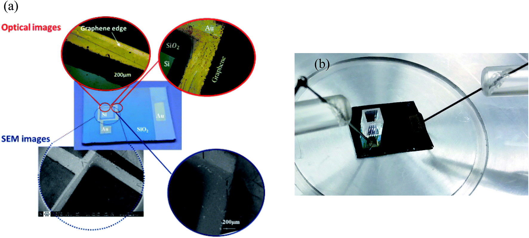 | ||
| Fig. 2 (a) SEM and optical images of the fabricated sensor. Images in the circles show the magnified view of the different parts of the device. (b) An optical image of the measurement setup including the sample with a cuvette placed on the graphene/Si junction. | ||
The transferred graphene on the Si/SiO2 substrate was analyzed by Raman spectroscopy, and the result is shown in Fig. 3. The G-band (1584 cm−1) and 2D-band (2673 cm−1) Raman peaks of graphene can be seen in this figure. The high peak intensity ratio of 2D to G obtained via this analysis indicates high crystallinity and monolayer nature of the graphene sheet.25
 | ||
| Fig. 3 Raman spectrum of the transferred graphene sheet on the Si/SiO2 substrate. | ||
As abovementioned, the graphene/Si junction behaves as a Schottky diode. Our fabricated device was then utilized for the sensing of BSA via monitoring of the electrical behavior of the graphene/Si Schottky junction under UV light irradiation. The electrical behavior of the device in the dark and under UV light irradiation is illustrated in Fig. 4a. The I–V characteristic of the fabricated device shows a rectifying behavior, confirming the formation of the Schottky junction at the interface of graphene/Si. Fig. 4a demonstrates that exposure of the fabricated device to UV light leads to a significant increment in the reverse bias current of the device. This increment in the reverse bias current due to the light exposure confirms high photo-response of the graphene/Si-based device. The light spectrum of the LED monochromatic UV source used in this experiment is provided in the inset of Fig. 4a.
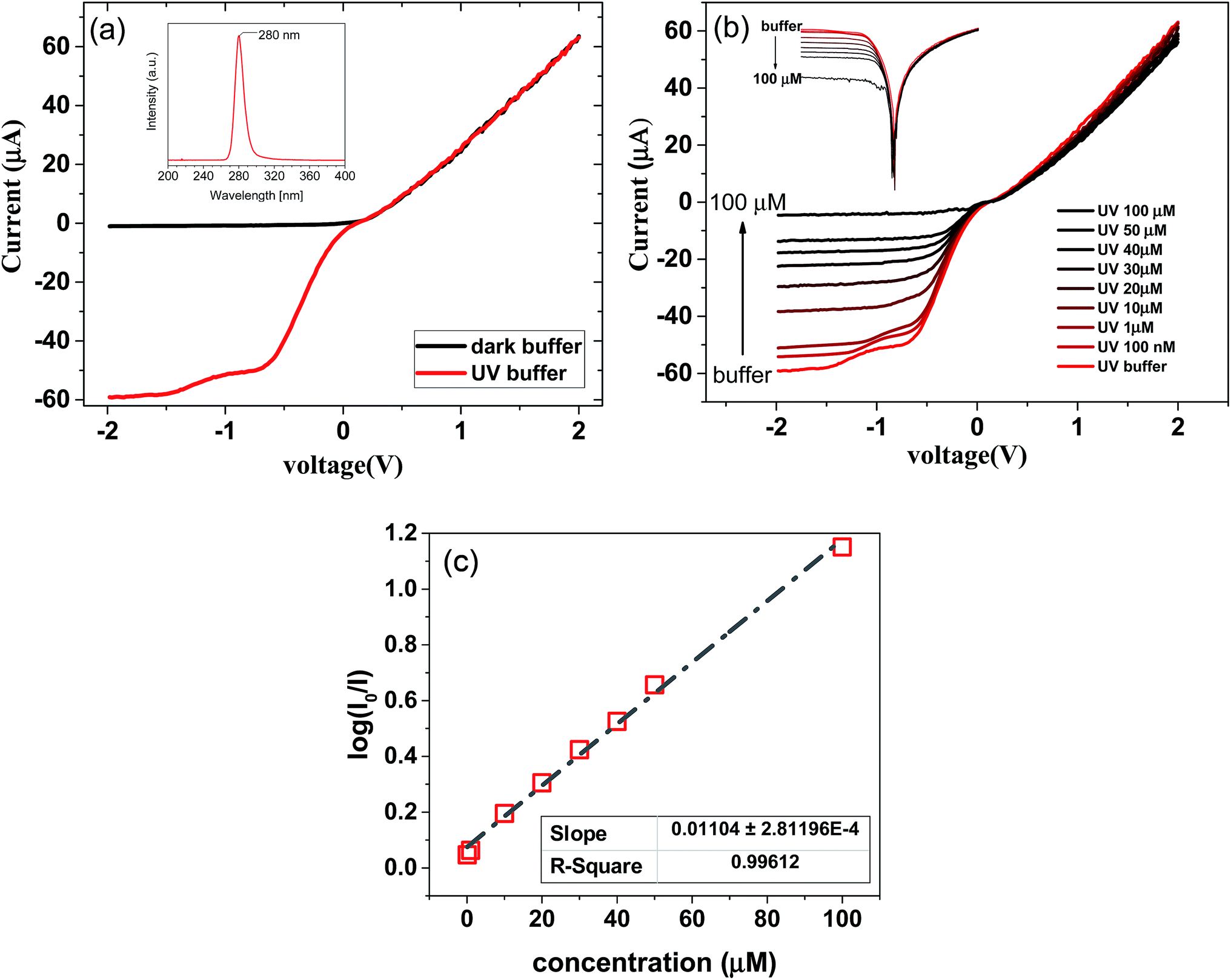 | ||
| Fig. 4 (a) I–V characteristic of the device in the dark and under UV light irradiation (the surface of the device was covered with the buffer in both measurements). The top inset shows the applied UV light spectra (b). I–V characteristic of the device under the 280 nm UV light exposure. BSA at different concentrations (100 nM to 100 μM) significantly affects the saturation current of the device. Top inset shows the semi-logarithmic plot. (c) The semi-logarithmic plot of the sensitivity of the device versus the BSA concentration. (The voltage bias used for this plot was −1.5 V.) | ||
To apply BSA in a buffer solution onto the device, a small open-base cuvette was directly placed on the device such that the solution covered the entire Si/graphene area. Fig. 4b shows the output characteristic of the device when it was exposed to BSA at different concentrations diluted in phosphate-buffered saline (PBS, pH 7.4) (PBS and BSA were obtained from Sigma-Aldrich, Germany) under UV light exposure. The analyte was exchanged by rinsing the sensor with solvent and blow-drying with nitrogen.
An increase in the BSA concentration leads to a decrement in the forward bias current of the device. This decrement can be explained by considering the electron-donating behavior of BSA that leads to charge concentration difference between the pristine and doped graphene. When graphene was exposed to electron donors, extra electrons were provided, causing an increase in the sheet resistance of graphene. As abovementioned, we have used pH 7.4 for the preparation of different concentrations of BSA. The isoelectric point of BSA is 5.4.26 Therefore, BSA behaves as an electron donor on the graphene surface. Moreover, pristine graphene is a p-type semiconductor because of the absorption of moisture or oxygen and PMMA residues. When the graphene surface is exposed to BSA, the Fermi level of graphene is shifted to the Dirac point; this causes an increase in the sheet resistance of graphene. As a result, upon increasing the BSA concentration, the forward current of the junction decreases.
Interestingly, it can be seen that the reverse bias current significantly changes under exposure to BSA at different concentrations. It has been reported that the graphene/Si Schottky junction is highly sensitive in the UVB region.27 Thus, UV light exposure leads to an increase in the reverse bias current of the device. When the graphene/Si junction is exposed to UV light, the incident photons generate electron–hole pairs in the structures. By applying a reverse bias, the generated electron–hole pairs are separated, and the injected holes in the graphene lead to a significant photocurrent.19,28 On the other hand, when the graphene/Si area is covered with the BSA solution, a decrement in the UV light absorption of the junction occurs because of the absorption of light by albumin. As shown in Fig. 4b, an increase in the BSA concentration leads to a decrease in the reverse bias current of the device. Based on their chemical composition, the chemical species absorb light at a particular wavelength (at 280 nm in the case of BSA). This light absorption obeys the Beer–Lambert law. On the other hand, the optical response of the graphene/Si photodiode is linear.29 Accordingly, log(I0/I) versus the BSA concentration has a linear response, as shown in the inset of Fig. 4c. The current detection limit in our experiment was 10 nA. According to the results shown in Fig. 4, the detection limit for the BSA protein is about 0.25 nM, which is the same order of magnitude or even better than that of the reported sensors.30,31 Note that we did not use any conjugated nanoparticles or markers for sensing; moreover, the sample was not manipulated and could be reused after testing.
The rectifying current–voltage characteristics of the Schottky diode can be expressed by the thermionic emission model in which the diode current can be written as follows:24
 | (1) |
 | (2) |
To monitor the light absorption spectra of BSA, BSA at different concentrations in the buffer solution was examined by a spectrometer (Avantes 2048 spectrometer), and the results are provided in Fig. 5. As shown in this figure, the maximum absorption wavelength of BSA is around 280 nm.
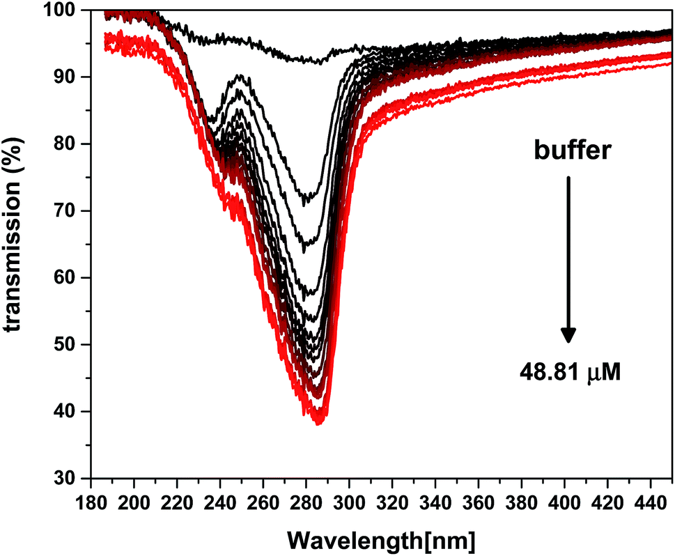 | ||
| Fig. 5 Absorption spectra of BSA at different concentrations. | ||
The real time measurement of the reverse bias current of the device for different concentration of BSA is plotted in Fig. 6a. Sensitivity as high as 0.5 A M−1 obtained by this graphene-based device makes it a promising candidate for accurate measurements in bio-sensing applications. The real-time response of the device to UV light exposure for BSA at different concentrations is also provided in Fig. 6b. The fast response to UV light is a normal behavior of the photodiodes. The rising time for this device is approximately 500 ms (Fig. 6c). An increase in the BSA concentration decreases the photoresponse of the device.
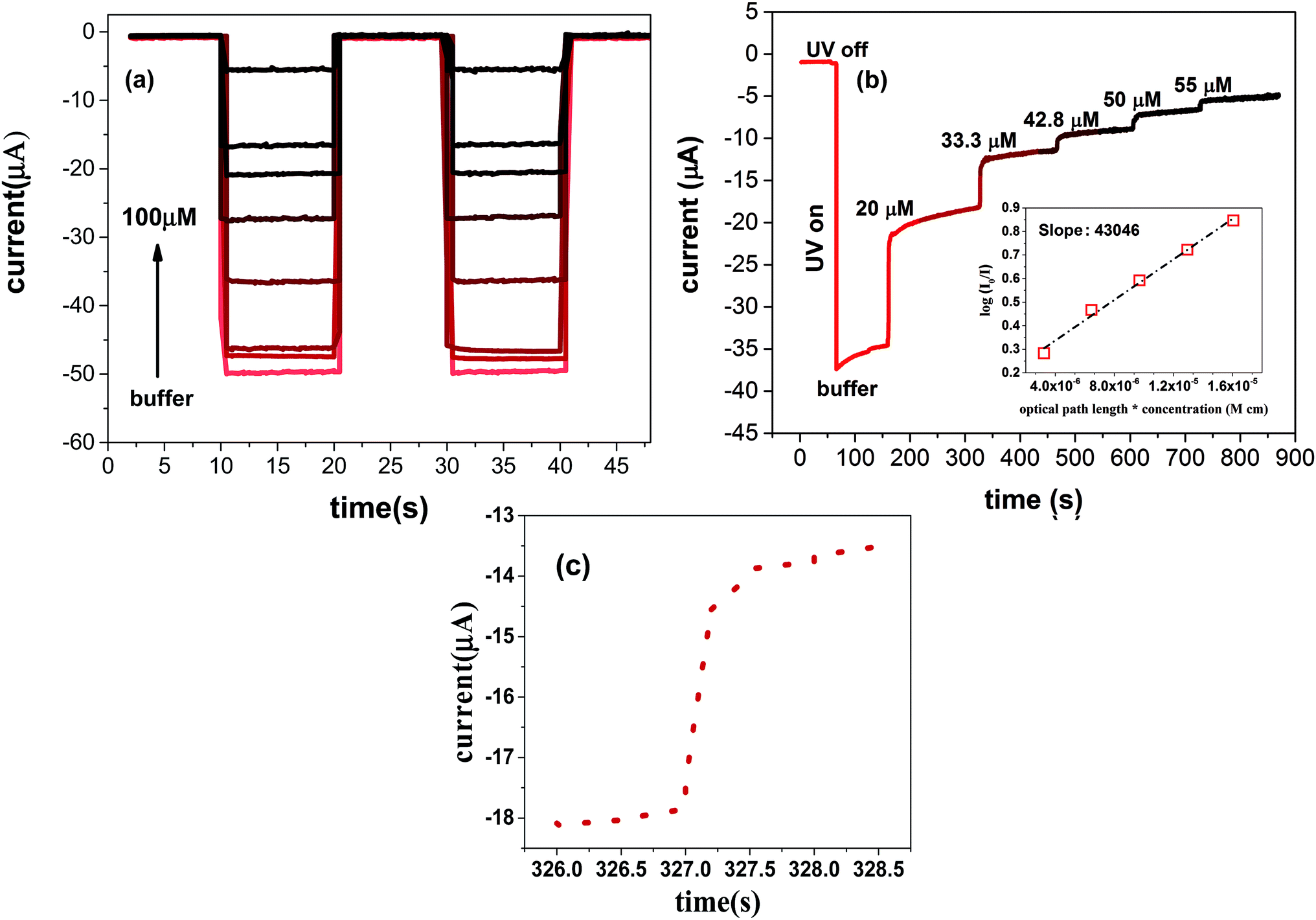 | ||
| Fig. 6 (a) Reverse bias current of the device versus time when exposed to BSA at different concentrations. (b) Real-time response of the device to UV light exposure for BSA at different concentrations. (c) Response time for the real time measurement. | ||
Output characteristics of the device near the zero voltage are shown in Fig. 7. As shown in this figure, the fabricated BSA detector has a diode current higher than 3 μA at zero voltage, confirming the self-powered properties of the device that would reduce the need for batteries. It can be seen from this figure that the zero voltage current of the device changes significantly when the device is exposed to BSA at different concentrations.
 | ||
| Fig. 7 I–V characteristic of the device under UV light exposure confirming the self-powered response of the device. | ||
Moreover, we calculated the responsivity and detectivity of the device for BSA at different concentrations. The responsivity is defined as the ratio of photocurrent to incident optical power irradiated on the device.32
 | (3) |
In the eqn (3), EQE, h, and υ are the external quantum efficiency, Planck's constant and frequency of incident light, respectively. The specific detectivity D* is calculated by the following equation:33
 | (4) |
| Buffer | 100 nM | 1 μM | 10 μM | 20 μM | 30 μM | 40 μM | 50 μM | 100 μM | |
|---|---|---|---|---|---|---|---|---|---|
| Photocurrent (μA) | 59.13 | 56.87 | 51.67 | 39.21 | 30.01 | 22.95 | 18.56 | 14.76 | 7.14 |
| Responsivity (mA W−1) | 202 | 191 | 176 | 134 | 102 | 78 | 64 | 50 | 24 |
| Detectivity (cm W−1 Hz1/2 × 1010) | 12 | 11.2 | 10.3 | 7.9 | 6 | 4.6 | 3.78 | 2.95 | 1.71 |
Currently, the use of mobile devices for biosensing and the point-of-care testing are the main approaches in the biosensing platform. The use of mobile and small devices, which just need a small sample volume to perform the measurement, for biological analysis offers numerous benefits such as rapid detection, reliable test results and simplicity. The graphene/Si-based device as a low cost, low power, sensitive, mobile and small device is actually the best candidate for protein sensing applications.
4. Conclusion
Herein, a graphene/Si-based Schottky diode was successfully fabricated and utilized for sensing BSA in a buffer solution. The device is very sensitive in the UVB region, and BSA effectively absorbs light in the UVB region. Using these features, we proposed a UVB-driven BSA sensor based on the graphene-Si junction. The output characteristic of the device during exposure to BSA showed that an increase in the BSA concentration leads to a decrease in the reverse bias current of the diode significantly. BSA has a significant light absorption around 280 nm. Consequently, when the Si/graphene area is covered by the BSA solution, a decrement in the UV light absorption of the junction occurs, leading to a decrease in the reverse bias current of the device. The sensitivity as high as 0.5 A M−1 and the detection limit of 0.25 nM obtained by monitoring the reverse bias current of the fabricated device indicate good performance of the introduced graphene-based diode for bio-sensing applications. In addition, the hybrid graphene-Si exhibits a wide detection range (from 100 nM to 100 μM). The output characteristic of the sensor at the zero bias showed self-powered properties of the device that would reduce the need for batteries. This capability in addition to the simplicity of device fabrication as well as its operating mechanism and high sensitivity is very important in the field of on-chip bio-sensing applications.Conflicts of interest
There are no conflicts to declare.Acknowledgements
The partial financial support of the Iran National Science Foundation (INSF) is acknowledged.References
- E. Singh, M. Meyyappan and H. S. Nalwa, Flexible graphene-based wearable gas and chemical sensors, ACS Appl. Mater. Interfaces, 2017, 9, 34544–34586 CrossRef CAS PubMed.
- T. Chen, Y. Sheng, Y. Zhou, R. J. Chang, X. Wang, H. Huang, Q. Zhang, L. Hou and J. H. Warner, High Photoresponsivity in Ultrathin 2D Lateral Graphene: WS2: Graphene Photodetectors Using Direct CVD Growth, ACS Appl. Mater. Interfaces, 2019, 11, 6421–6430 CrossRef CAS PubMed.
- C. I. Justino, A. R. Gomes, A. C. Freitas, A. C. Duarte and T. A. Rocha-Santos, Graphene based sensors and biosensors, TrAC, Trends Anal. Chem., 2017, 91, 53–66 CrossRef CAS.
- A. Y. Zhu, J. C. Fei Yi, H. Z. Reed and C. Ertugrul, Optoelectromechanical multimodal biosensor with graphene active region, Nano Lett., 2014, 14, 5641–5649 CrossRef CAS PubMed.
- Y. Ohno, M. Kenzo, Y. Yusuke and M. Kazuhiko, Electrolyte-gated graphene field-effect transistors for detecting pH and protein adsorption, Nano Lett., 2009, 9, 3318–3322 CrossRef CAS PubMed.
- M. Nurunnabi, K. Parvez, M. Nafiujjaman, V. Revuri, H. A. Khan, X. Feng and Y. K. Lee, Bioapplication of graphene oxide derivatives: drug/gene delivery, imaging, polymeric modification, toxicology, therapeutics and challenges, RSC Adv., 2015, 5, 42141–42161 RSC.
- B. Zhang and T. Cui, Suspended Graphene Nanoribbon Ion-Sensitive Field-Effect Transistors Formed by Shrink Lithography for pH/Cancer Biomarker Sensing, J. Microelectromech. Syst., 2013, 22, 1140–1146 CAS.
- S. Srivastava, S. Abraham, C. Singh, M. A. Ali, A. Srivastava, G. Sumana and B. D. Malhotra, Protein conjugated carboxylated gold@reduced graphene oxide for aflatoxin B1 detection, RSC Adv., 2015, 5, 5406–5414 RSC.
- W. Yue, C. Tang, C. Wang, C. Bai, S. Liu, X. Xie, H. Hua, Z. Zhang and D. Li, An electricity-fluorescence double-checking biosensor based on graphene for detection of binding kinetics of DNA hybridization, RSC Adv., 2017, 7, 44559–44567 RSC.
- S. Xu, J. Zhan, B. Man, S. Jiang, W. Yue, S. Gao, C. Guo, H. Liu, Z. Li, J. Wang and Y. Zhou, Real-time reliable determination of binding kinetics of DNA hybridization using a multi-channel graphene biosensor, Nat. Commun., 2017, 8, 14902–14912 CrossRef CAS PubMed.
- A. Huang, W. Li, S. Shi and T. Yao, Quantitative fluorescence quenching on antibody-conjugated graphene oxide as a platform for protein sensing, Sci. Rep., 2017, 7, 40772–40783 CrossRef CAS PubMed.
- H. Polet and H. Spieker-Polet, Serum albumin is essential for in vitro growth of activated human lymphocytes, J. Exp. Med., 1975, 142, 949–959 CrossRef CAS PubMed.
- L. Zhu, C. S. Lee and D. L. DeVoe, Integrated microfluidic UV absorbance detector with attomol-level sensitivity for BSA, Lab Chip, 2005, 6, 115–120 RSC.
- D. L. Rupert, C. Lässer, M. Eldh, S. Block, V. P. Zhdanov, J. O. Lotvall, M. Bally and F. Höök, Determination of exosome concentration in solution using surface plasmon resonance spectroscopy, Anal. Chem., 2014, 86, 5929–5936 CrossRef CAS PubMed.
- B. J. Olson and J. Markwell, Assays for determination of protein concentration, Curr. Protoc. Protein Sci., 2007, 48, 3–4 Search PubMed.
- P. Lv, X. Zhang, X. Zhang, W. Deng and J. Jie, High-sensitivity and fast-response graphene/crystalline silicon Schottky junction-based near-IR photodetectors, IEEE Electron Device Lett., 2013, 34, 1337–1339 CAS.
- S. Riazimehr, A. Bablich, D. Schneider, S. Kataria, V. Passi, C. Yim, G. S. Duesberg and M. C. Lemme, Spectral sensitivity of graphene/silicon heterojunction photodetectors, Solid-State Electron., 2016, 115, 207–212 CrossRef CAS.
- G. Luongo, F. Giubileo, L. Genovese, L. Iemmo, N. Martucciello and A. Di Bartolomeo, IV and CV characterization of a high-responsivity graphene/silicon photodiode with embedded MOS capacitor, Nanomaterials, 2017, 7(7), 158–166 CrossRef PubMed.
- A. Di Bartolomeo, G. Luongo, L. Iemmo, F. Urban and F. Giubileo, Graphene–Silicon Schottky Diodes for Photodetection, IEEE Trans. Nanotechnol., 2018, 17(6), 1133–1137 Search PubMed.
- L. Lin, L. Liao, J. Yin, H. Peng and Z. Liu, Building graphene p–n junctions for next-generation photodetection, Nano Today, 2015, 10, 701–716 CrossRef CAS.
- X. An, F. Liu, Y. J. Jung and S. Kar, Tunable graphene–silicon heterojunctions for ultrasensitive photodetection, Nano Lett., 2013, 13, 909–916 CrossRef CAS PubMed.
- A. Hekmatikia and Y. Abdi, Graphene–Silicon-Based High-Sensitivity and Broadband Phototransistor, IEEE Electron Device Lett., 2018, 39, 216–219 CAS.
- M. A. Sakr and M. Serry, Non-enzymatic graphene-based biosensors for continuous glucose monitoring, IEEE Sens. J., 2015, 1–4 Search PubMed.
- H. Y. Kim, K. Lee, N. McEvoy, C. Yim and G. S. Duesberg, Chemically modulated graphene diodes, Nano Lett., 2013, 13, 2182–2188 CrossRef CAS PubMed.
- A. C. Ferrari, J. C. Meyer, V. Scardaci, C. Casiraghi, M. Lazzeri, F. Mauri, S. Piscanec, D. Jiang, K. S. Novoselov, S. Roth and A. K. Geim, Raman spectrum of graphene and graphene layers, Phys. Rev. Lett., 2006, 97, 187401–187407 CrossRef CAS PubMed.
- Y. Ohno, K. Maehashi and K. Matsumoto, Chemical and biological sensing applications based on graphene field-effect transistors, Biosens. Bioelectron., 2010, 26(4), 1727–1730 CrossRef CAS PubMed.
- X. Wan, Y. Xu, H. Guo, K. Shehzad, A. Ali, Y. Liu, J. Yang, D. Dai, C. T. Lin, L. Liu and H. C. Cheng, A self-powered high-performance graphene/silicon ultraviolet photodetector with ultra-shallow junction: breaking the limit of silicon?, npj 2D Mater. Appl., 2017, 1, 4–12 CrossRef.
- A. D. Bartolomeo, G. Luongo, F. Giubileo, N. Funicello, G. Niu, T. Schroeder, M. Lisker and G. Lupina, Hybrid graphene/silicon Schottky photodiode with intrinsic gating effect, 2D Materials, 2017, 4(2), 025075 CrossRef.
- X. Li, M. Zhu, M. Du, Z. Lv, L. Zhang, Y. Li, Y. Yang, T. Yang, X. Li, K. Wang and H. Zhu, High Detectivity Graphene-Silicon Heterojunction Photodetector, Small, 2015, 12, 595–601 CrossRef PubMed.
- C. Wang, Y. Zhou, K. X. Zhang, X. G. Nie and X. H. Xia, Fast and sensitive detection of protein concentration in mild environments, Talanta, 2015, 135, 102–107 CrossRef CAS PubMed.
- A. Urrutia, K. Bojan, L. Marques, K. Mullaney, J. Goicoechea, S. James, M. Clark, R. Tatam and S. Korposh, Novel highly sensitive protein sensors based on tapered optical fibres modified with Au-based nanocoatings, J. Sens., 2016, 8129387 Search PubMed.
- A. Di. Bartolomeo, Graphene Schottky diodes: an experimental review of the rectifying graphene/semiconductor heterojunction, Phys. Rep., 2016, 606, 1–58 CrossRef.
- V. Dhyani and S. Das, High-speed scalable silicon-MoS2 PN heterojunction photodetectors, Sci. Rep., 2017, 7, 44243 CrossRef PubMed.
| This journal is © The Royal Society of Chemistry 2019 |