
 Open Access Article
 This Open Access Article is licensed under a Creative Commons Attribution-Non Commercial 3.0 Unported Licence
Enhanced photoelectrochemical performance of TiO2 nanorod array films based on TiO2 compact layers synthesized by a two-step method
Yafeng Deng a,
Zhanhong Maa,
Fengzhang Ren*ab and
Guangxin Wangac
a,
Zhanhong Maa,
Fengzhang Ren*ab and
Guangxin Wangac
aSchool of Materials Science and Engineering, Henan University of Science and Technology, Luoyang, 471023, P. R. China. E-mail: dengyf1111@126.com; renfz@haust.edu.cn
bHenan Collaborative Innovation Centre of Non-Ferrous Generic Technology, Luoyang, 471023, P. R. China
cHenan Key Laboratory of Non-Ferrous Materials Science & Processing Technology, Luoyang, 471023, P. R. China
First published on 15th July 2019
Abstract
An innovative two-step method perfectly prepared TCLs with different thicknesses, and then the TNA films based on TCLs were successfully prepared. The effects of different thicknesses of TCLs on the morphology and photoelectrochemical performance of TNA films were investigated. The results indicated that TCLs with appropriate thickness could effectively improve the morphology and photoelectrochemical performance of TNA films. Compared with the TNA films based on TCL5, TCL10 and TCL30, the TNA film based on TCL20 exhibited more ideal and comprehensive photoelectrochemical performance. Moreover, dye-sensitized solar cells (DSSCs) based on this TNA film achieved the highest Jsc (10.2054 mA cm−2), Voc (0.5737 V), PCE (3.3%) and Pout (3.31 mW cm−2).
Introduction
As the third-generation solar cells, non-pn junction thin film solar cells have become an important research field in the world. Its typical representatives include Perovskite solar cells (PSCs),1–4 dye-sensitized solar cells (DSSCs),5–8 and quantum dots-sensitized solar cells (QDSCs).9–12 Among them, a huge application potential of DSSCs relies on their advantages, such as lower cost,, light weight, effective use of diffuse light, better performance under weak light, and possibility to form flexible cells and to be designed double-sided or with multi-color appearance. In addition, with the in-depth study of DSSC basic theory, the performance of the cells will be further improved to become practical solar cells with low-cost and high photoelectric conversion efficiency. As the key electron transport layer material, the photoanode plays an important role in the final performance of DSSCs. Common electron transport layer materials include TiO2,13,14 ZnO,15,16 SnO2 (ref. 17 and 18) and Nb2O5.19,20 As a typical wide-band gap transition metal oxide semiconductor (MOS) material, TiO2 has excellent physical and chemical properties. TiO2 with its high chemical stability, appropriate band gap, good photoelectric conversion performance, excellent charge separation and transmission capacity, as well as low-price, non-toxicity and abundant reserves, has always been the research emphasis for electron transport layer materials.21–25As typical TiO2 materials, the one-dimensional TiO2 materials have been extensively studied. Currently, the main methods for the preparation of the one-dimensional TiO2 nanomaterials include hydrothermal,26,27 anodic oxidation28,29 and template method,30 among which the hydrothermal method is the most commonly used. On the one hand, the hydrothermal method can directly grow one-dimensional TiO2 nanomaterials on a conductive substrate, which are firmly combined with the substrate and well oriented. On the other hand, the hydrothermal method presents the advantages, such as low-cost, short synthesis cycle, process simplicity as well as easy realization and regulation of reaction conditions. As the electron transport layer materials, the one-dimensional TiO2 nanomaterials can not only reduce the band edge, surface state and crystal defects but also effectively enhance the light-scattering effect of the photoanode.31–35 Moreover, the one-dimensional nanomaterials provide a nearly linear transmission path for electrons, which greatly shortens the electron transport distance, prolongs the electron lifetime, reduces the charge recombination, thereby improving the carrier quantum yield and laying a foundation for the good photoelectric performance of solar cells.36,37 However, the nucleation type of TiO2 nanorods formed on the bare FTO substrate is a primary nucleation, in which the system does not contain substances to be crystallized. There is a certain lattice mismatch between the TiO2 crystal and the SnO2 crystal in the substrate. Thus, to crystallize TiO2 on the FTO substrate it has to overcome the large energy barrier caused by the lattice mismatch, which adversely affects the crystal growth of TiO2 nanorods. Moreover, the nucleation type of TiO2 nanorods based on TiO2 compact layers (TCLs) follows the secondary nucleation, i.e. the system contains substances to be crystallized at the time of nucleation. Since there is no lattice mismatch, TiO2 is more susceptible to the nucleation crystallization on TCLs and the effect of TCLs on the growth of TiO2 crystal will eventually have a certain impact on the photoelectrochemical performance of TiO2 nanorods.38–40
Herein, the innovative two-step method was used to prepare perfect TCLs with different thicknesses. The FTO substrate with TCL was named as FTOTCL. In previous studies, TCLs were mostly synthesized by liquid phase deposition,27,41 spin-coating,39,42 atomic layer deposition43,44 and sol–gel process.45,46 However, the liquid phase deposition and atomic layer deposition have high technical operation requirements; moreover, these processes are complex and their cost is high. Spin-coating and sol–gel coating are easy to be realized, but the coating effect is poor. Therefore, we innovatively proposed a two-step method, which is simple and low-cost while guaranteeing a good film-forming effect. Completely different from the mentioned methods, in this study, the first step in preparing TCL was to deposit a nano-metal Ti compact layer on the FTO substrate by a magnetron sputtering technology, and the second step was to transform the nano-metal Ti compact layer into the required TCL by an oxidation treatment under certain conditions (the TCLs based on different magnetron sputtering times were defined as TCL5, TCL10, TCL20 and TCL30). Then, a layer of well-crystallized one-dimensional TiO2 nanorod array film (TNA film) based on the TCL was grown by the hydrothermal method as electron transport layer. The samples were characterized by field emission scanning electron microscopy (FESEM), X-ray diffraction (XRD), UV-Vis spectroscopy, photoluminescence (PL) spectroscopy, electrochemical impedance spectroscopy (EIS), Bode plots and Mott–Schottky plots. The effects of TCLs with different thicknesses prepared by changing the magnetron sputtering time on TNA films were studied. The results showed that TNA films based on the TCL20 obtained better and comprehensive photoelectrochemical properties, and thus the DSSCs based on this TNA film achieved the highest Jsc (10.2054 mA cm−2), Voc (0.5737 V), PCE (3.3%) and Pout (3.31 mW cm−2).
Experimental
Materials
Pure titanium target (φ50 × 4 mm, ≥99.995%) was purchased from the Deyang ONA New Materials Co., Ltd. F-doped SnO2 transparent conductive glass (FTO, 30 × 30 × 2.2 mm, square resistance ≤ 7 Ω □−1, transmittance ≥ 80%) was purchased from the South China Science & Technology Co., Ltd. Tetrabutyl titanate (≥98%), titanium tetrachloride (≥98%), hydrochloric acid (36–38 wt%), anhydrous ethanol (≥99.7%), acetone (≥99.5%), isopropanol (≥99.7%), tert-butyl alcohol (TBA, ≥99.7%) and acetonitrile (≥99.5%) were purchased from the Sinopharm Chemical Reagent Co., Ltd. Di-tetrabutylammonium cis-bis (isothiocyanato) bis (2,2′-bipyridyl-4,4′-dicarboxylato) ruthenium(II) (N719, ≥99%), lithium iodide (99.9% trace metals basis), iodine (≥99.99% trace metals basis), 4-tert-butyl pyridine (TBP, 96%) and surlyn polymer frame (25 μm) were purchased from Shanghai Aladdin Bio-Chem Technology Co., Ltd. Gold counter-electrode and deionized water were made in our laboratory. The FTO was washed with acetone, isopropanol and deionized water before use.Synthesis of TiO2 compact layers
Step one: the pure Ti compact layer was sputtered on FTO glass substrate using a magnetron sputter coater.47 The chamber consisted of a rotating substrate holder with adjustable height and a 50 mm diameter target-base. A water-cooling system was used. The pure Ti compact layer was deposited using a pure Ti target (99.995%) with a high purity Ar (99.99%) at room temperature. The base pressure in the chamber prior to any deposition was 4 × 10⁻⁴ Pa. For pure Ti compact layer deposition the target–substrate distance was 80 mm, the sputtering power was 125 W, the flow rate of argon was kept at a constant value of 43 sccm, and the sputtering pressure was kept at 0.55 Pa during the deposition. The target was presputtered for 10 min prior to sputtering to remove the oxide layer from the target surface. The sputtering time was varied between 5 and 30 min.Step two: the pure Ti compact layers were transformed into TiO2 compact layers by oxidation treatment. The pure Ti compact layers were sputtered on FTO glass substrate and were placed in a muffle furnace and oxidized at 550 °C for a period of time in a nitrogen-oxygen mixed atmosphere (N2/O2, v/v, 4/1). Then, the oxidized compact layers were treated in a 50 mM TiCl4 aqueous solution at 80 °C for a period of time, and washed with deionized water to obtain TCL5, TCL10, TCL20 and TCL30.
Synthesis of TiO2 nanorods array films
A mixed solution of concentrated hydrochloric acid and deionized water (v/v, 1/1, 60 mL) was taken, and then 1 mL tetrabutyl titanate was slowly added to the hydrochloric acid aqueous solution at a rate of about 1 drop per 3 s with continuous vigorous stirring to avoid the hydrolysis of tetrabutyl titanate until the solution was clear and transparent. The prepared FTOTCL was placed in a Teflon liner (50 mL) at an angle of 45–60° to the vertical wall and the as-prepared solution was poured into the Teflon liner and sealed; then, the reactor was placed at a constant temperature in an oven at 150 °C for the hydrothermal reaction.48 After that, the FTOTCL was removed and washed several times with absolute ethanol and deionized water, and then the dried FTOTCL was annealed in a muffle furnace at 450 °C for a period of time to obtain the TNA film.Fabrication of DSSCs
For the fabrication of DSSCs, TNA film photoanodes were dipped in N719 dye ethanol/TBA (v/v, 1/1) solution (5 × 10⁻⁴ M) for 24 h. Then, the photoanodes were withdrawn from the solution and dried under a stream of argon. A gold counter-electrode and a dye-coated photoanode were, then, put together with the surlyn polymer frame and heated at 110 °C to adhere to the electrodes. The electrolyte consisted of 0.05 M I2, 0.5 M LiI and 0.5 M tert-butyl pyridine in acetonitrile.Characterization
The morphology of the samples was examined by the field-emission scanning electron microscopy (FESEM, JSM-7800 F, JEOL). The X-ray diffraction data was acquired using a Bruker D8 Advance powder X-ray diffractometer (XRD, Bruker) with the X-ray tube producing Cu Kα radiation (λ = 1.5406 Å) and the generator set at 40 kV and 40 mA during data collection. Data was collected from 20–80° (2θ). A UV-visible spectrophotometer (UV-2600, Shimadzu) was utilized to obtain the transmittance spectra and absorption spectra of the TNA films. The photoluminescence (PL) experiments were performed using a WFY-28 Fluorescence spectrophotometer (Tianjin Tuo Pu Instrument Co., Ltd). The EIS, Bode plots and Mott–Schottky plots were measured by an electrochemical workstation (CHI660D, Beijing Join Technology Co., Ltd) at a bias of 0.3 V with the frequency sweeping from 1 Hz to 0.1 MHz, and the data were fitted using ZSimpWin software. A solar simulator was used for I–V measurements (AM1.5G, 100 mW cm−2, SolarIV, Beijing Zolix Instruments Co., Ltd), which was calibrated by a 91150-KG5 reference cell (Newport, USA). All samples were measured at room temperature.Results and discussion
Morphology and structure
Fig. 1a–d represent the FESEM images of the TNA films grown over different TCLs. It can be seen from the side-views of TNA films that all TiO2 nanorods grew perpendicular to the substrate and the bottom end of nanorods is tightly bonded to the substrate; however, the morphology of TiO2 nanorods is significantly different for different TCLs. The TiO2 nanorods prepared on TCL5 and TCL10 (Fig. 1a and b) are loose and uneven. Moreover, the TiO2 nanorod fragmentation is serious, which significantly reduces the overall compactness of the TNA films, destroys the array structure of TiO2 nanorods and results in the increase of crystal defects, namely, interface and surface states, and then impedes the transfer of charge in the TNA films and adversely affects the photoelectric performance of TNA films. However, the TiO2 nanorods grown over TCL20 (Fig. 1c) are closely connected with each other, uniform and compact, orderly arranged and without fragmentation, which indicates the good crystal integrity of TiO2 nanorods and has a positive effect on the reduction of crystal defects in the TNA films. Furthermore, the combined action of dense TNA films and TCL20 in DSSCs can effectively prevent the direct contact between the conductive layer of FTO and the redox electrolyte to reduce the dark current.28 In Fig. 1d, the top-view of TiO2 nanorods grown over TCL30 shows tetragonal rod-like morphology. However, side-view shows that the TiO2 nanorods below their middles have fused together and are irregular and fragmented, which can seriously damage the array structure of TNA films and affect their charge transfer performance. In addition, the compactness of TNA films also decreases significantly.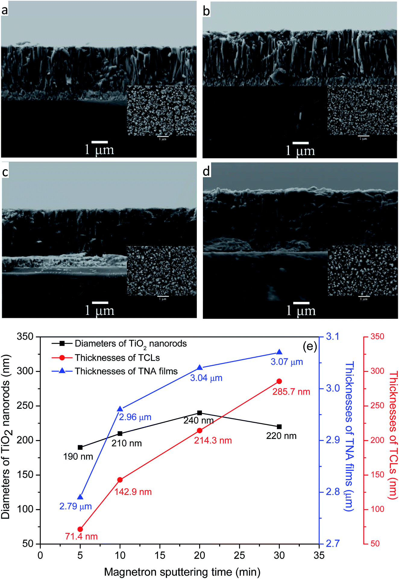 | ||
| Fig. 1 FESEM images of various TNA films grown over different TCLs: (a) TCL5, (b) TCL10, (c) TCL20, (d) TCL30, and (e) the thicknesses of TCLs, thicknesses of TNA films and diameters of TiO2 nanorods. | ||
In Fig. 1e, the thicknesses of TNA films increases with the increase in the thicknesses of TCLs, but the rate of increase gradually decreased (6.09%, 2.70%, 0.99%), which indicates that TCLs had a diminishing influence on the thicknesses of the TNA films. The average diameter of TiO2 nanorods first increases and reaches a maximum (at about 240 nm) with magnetron sputtering for 20 min, and then the diameter decreases. However, the increase in the average diameter of TiO2 nanorods (10.53%, 14.29%, and −8.33%) is greater than the increase in the thicknesses of the TNA films, indicating that the diameters of TiO2 nanorods are more susceptible to the TCLs. The increase in the diameter of the TiO2 nanorods increases the specific surface area of the TNA films, providing more active surface for the adsorption of the N719 dye, thereby enhancing the absorption of light by the TNA films.
Fig. 2 shows the XRD patterns of TNA films grown over different FTOTCL. The XRD patterns of TNA films contain seven peaks, five of which arise from the FTO substrate (JCPDS no. 77-452) and the other two diffraction peaks at 36.22° and 62.91° are assigned to the (101) and (002) planes of tetragonal rutile TiO2 (JCPDS no 65-192).49 As can be seen from Fig. 2a, the intensity of the (002) peak of TNA films is significantly enhanced, while the other diffraction peaks of TNA films become weak or even disappear. This is because TCLs can be used as the TiO2 seed layers to eliminate the lattice mismatch between TiO2 crystal and FTO substrate, thus, these TiO2 crystals can grow better over TCLs. The only (002) strong diffraction peak also proves that the TiO2 nanorods grow in the [001] direction with the growth axis parallel to the substrate surface normal.27,29 For TCL5, TCL10 and TCL20, the intensity of the (002) peak of TNA films gradually increases; however, for TCL30, it is the same as that for TCL20. This shows that the increasing thickness of TCLs can improve the crystallization performance of TiO2 to a certain extent and promote the better oriented crystallization growth of TiO2 nanorods. Fig. 2b demonstrates the partial XRD patterns of (002) peak. When compared with the (002) peak for TCL5, the other three (002) peaks shift 0.12° to the small angles (the effects of other error factors have been ruled out), making the 2θ of (002) peak more consistent with the standard tetragonal rutile TiO2. This shows that increasing the thickness of TCL can improve the crystal integrity of TiO2 nanorods and promote the growth of TiO2 crystals in accordance with the tetragonal rutile TiO2 lattice arrangement rules. This is because of the lattice mismatch between the TiO2 crystal and the SnO2 crystal in the FTO substrate. To eliminate this mismatch, a TiO2 prefabricated layer should be deposited between the TiO2 crystal and the SnO2 crystal in advance. However, the elimination of lattice mismatch is not an overnight process, but a gradual easing process. Only when the TiO2 prefabricated layer reaches a certain thickness, the lattice mismatch can be gradually alleviated and eliminated, and this TCL is the TiO2 prefabricated layer. Therefore, the maximum intensity of (002) diffraction peak and good morphology (Fig. 1c) of TNA films based on TCL20 has shown that this TCL thickness (214.3 nm, Fig. 1e) has well eliminated the effect of lattice mismatch for the directional growth of TiO2 crystals.
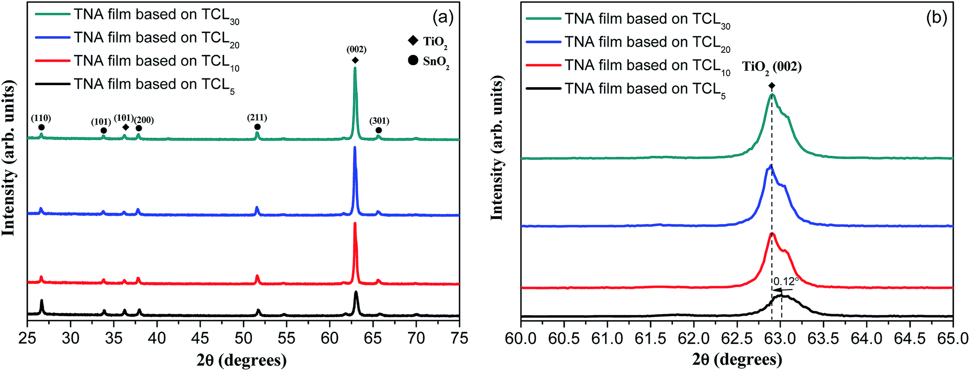 | ||
| Fig. 2 (a) XRD patterns of various TNA films grown on different TCLs and (b) the XRD patterns of (002) diffraction peak. | ||
Optical performance
The UV-Vis spectra of obtained TNA films were characterized as shown in Fig. 3. From Fig. 3a, the light absorption band edges of various TNA films grown over different TCLs are not significantly offset, which indicates that the crystal band-gap structure of TiO2 nanorods based on different TCLs has not changed. Moreover, the corresponding band-gaps (Eg, Fig. 3b) also change very little and are basically consistent with the Eg (3.03 eV) of the standard tetragonal rutile TiO2. This is because the purpose of this study was to introduce TCLs by the two-step method and to prepare well-crystallized TiO2 nanorods. Since both are composed of the same pure TiO2 crystal, there is no change in the crystal structure or phase and the light absorption band edges of all TNA films are basically the same. However, the absorbance of TNA films in the ultraviolet region is gradually enhanced with the increase in thicknesses of TCLs. Similarly, as the thickness of TCL increases, the transmittance of TNA films is significantly enhanced in the visible region, which allows more visible light through the TNA films for energy conversion in the N719 dye layers. This is mainly attributed to the fact that TCLs with certain thickness eliminate the lattice mismatch and promote the crystal integrity of TiO2 nanorod crystals, which reduces the morphological and structural defects of TiO2 nanorods and makes the TiO2 nanorod array more orderly, reducing the scattering of TNA films under visible light and allowing more visible light through TNA films to reach the light absorption layers. | ||
| Fig. 3 (a) Absorption spectrum, (b) Eg − (αhν)2 plots, (c) transmittance spectrum, and (d) PL spectrum of various TNA films grown over different TCLs. | ||
The photoluminescence spectra are commonly used to characterize electronic structures and electronic states in semiconductor materials. In Fig. 3d (the excitation wavelength is 260 nm), the shape of the PL spectrum of all TNA films is basically similar, which indicates that the energy level distribution of TiO2 crystals in all TNA films has no obvious change, and the distribution of the electronic state density of TiO2 crystals in the band-gaps is also basically similar.50 As shown in Fig. 3d, with the increase of TCL thickness, the PL intensity of TNA films decreases significantly, and the PL intensity of the TNA film based on TCL20 reaches the lowest value. This change is also attributed to the improvement in the crystallization performance of TiO2 nanorods caused by TCLs. The appropriate thicknesses of TCLs can improve the TiO2 crystal integrity, thus reducing the defect concentration in TiO2 crystals,51 which in turn reduces the charge recombination center caused by the defect, effectively separating the photogenerated electrons and holes. Since the charge recombination rate is lowered, the intensity of fluorescence generated by charge recombination is also lowered. Therefore, the maximum intensity of the (002) diffraction peak (Fig. 2a) and good morphology (Fig. 1c) of TNA films grown over TCL20 show that the lowest PL strength benefits from the well-crystallized TiO2 nanorod crystal. In addition, according to the position and intensity analysis of the PL peaks, the PL peak at 423.5 nm is the bound exciton peak with weak intensity, and the PL peak at 455 nm is its phonon peak. The sharp PL peak at 471.5 nm is a free exciton peak with strong intensity, and the latter two PL peaks at 486.5 nm and 496.5 nm are their phonon peaks.52 However, the blue shift of the bound exciton peak of TNA films grown over TCL20 from 423.5 nm to 416.5 nm is due to the crystal integrity of the TiO2 nanorods, which makes it difficult for photons with a wavelength of 423.5 nm to excite the bound exciton in the TiO2 crystals. When the photon wavelength blue shifts to 416.5 nm, the bound exciton absorbs the photon and is excited, and then generates the corresponding PL peak when it transitions back to the ground state.
Electrical performance
EIS was employed to investigate the charge transfer processes at various interfaces.53,54 Frequency sweeping test from 1 Hz to 0.1 MHz at a bias voltage of 0.3 V was applied. A 0.5 M Na2SO4 solution was used as the electrolyte, while platinum electrode, and saturated calomel electrode were used as the counter and reference electrodes, respectively. Fig. 4a presents the Nyquist plots of various TNA films grown over different TCLs. In the fitting circuit, Rs, Rct, Ric and Rrec are the liquid–solid interface resistance between the active electrode and electrolyte, charge transfer resistance, solid–solid interface resistance between TNA films and FTO substrate and charge recombination resistance, respectively. The fitting results of the Nyquist plots are shown in Table 1. According to the fitting results, the Rs, Rct and Ric of TNA films decrease significantly with the increase in the TCL thickness, which indicates that the charge transfer performance in different interfaces and thin films has been effectively improved, and the increase in Rrec further inhibits the charge recombination process. With the improvement in the charge transfer process and the reduction of charge recombination, the effective charge collection rate is improved, which lays a foundation for improving the current density of DSSCs. The Rct and Rrec of the TNA film grown over TCL20 achieve a minimum (22.7 Ω) and a maximum (4600 kΩ), indicating that this TNA film has a relatively better charge transfer performance. As the constant phase element (CPE), admittance (Y0) characterizes the conductivity of the film, and the larger the Y0, the better the conductivity. Moreover, n represents the physical properties of the element, which to some extent can represent the roughness or porosity of the film surface. The closer n is to 1, the smoother the film surface and the smaller the porosity. In Table 1, Y0 and n increase with the increase in the TCL thickness (from TCL5 to TCL20), following which the Y0 and n of TNA films grown over TCL30 reduce. It is shown that the TCL of appropriate thickness can significantly improve the conductivity and reduce the porosity of TNA films. Thus, the TNA film based on TCL20 not only has good conductivity but also has the smallest porosity, also confirming the observed better morphology in Fig. 1c.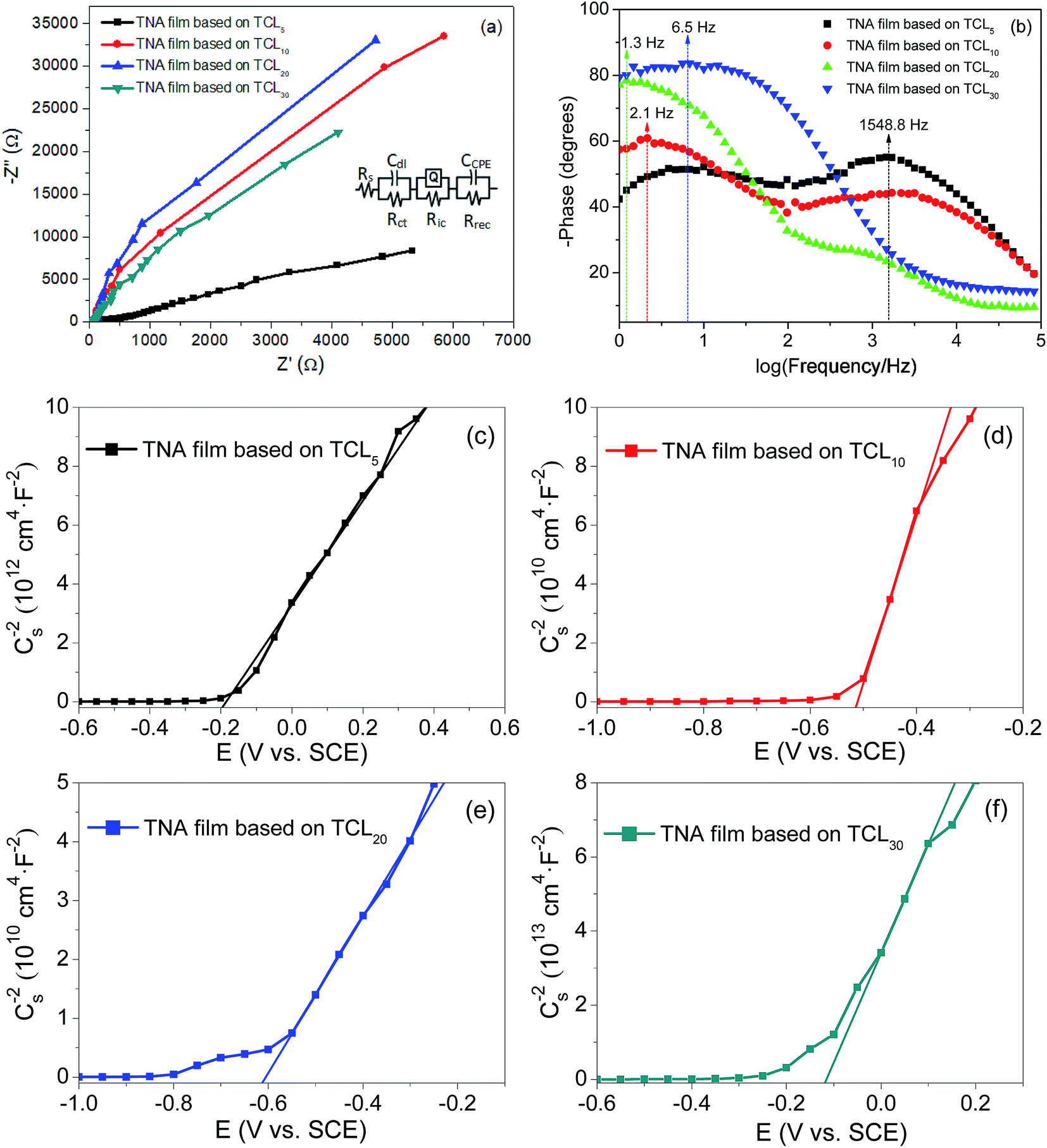 | ||
| Fig. 4 (a) Nyquist plots, (b) Bode plots, and (c)–(f) Mott–Schottky plots of various TNA films grown over different TCLs. | ||
| TNA films grown over | Rs (Ω) | Rct (Ω) | Ric (kΩ) | Rrec (kΩ) | Y0 (10−5 Ω−1 cm−2 sn) | n |
|---|---|---|---|---|---|---|
| TCL5 | 9.4 | 370.9 | 0.4 | 860 | 1.5 | 0.71 |
| TCL10 | 12.2 | 53.1 | 2800 | 1500 | 5.4 | 0.75 |
| TCL20 | 6.7 | 22.7 | 280 | 4600 | 4.6 | 0.85 |
| TCL30 | 5.6 | 32.9 | 39 | 3700 | 3.1 | 0.26 |
Fig. 4b shows the representative Bode plots of TNA films grown over different TCLs. The frequency peak is related to the electron transfer processes at various interfaces, and the electron lifetime (τe, Table 2) can be estimated from the Bode plots via the following equation:32
 | (1) |
| TNA films grown over | Efb (V vs. SCE) | ND (cm−3) | τe (ms) |
|---|---|---|---|
| TCL5 | −0.19 | 4.42 × 10¹⁶ | 0.11 |
| TCL10 | −0.51 | 1.38 × 10¹⁸ | 75.79 |
| TCL20 | −0.62 | 5.91 × 10¹⁸ | 122.43 |
| TCL30 | −0.12 | 2.66 × 10¹⁵ | 24.49 |
The results show that the increase in the TCL thickness greatly prolongs the electron lifetime, and τe of TNA film grown over TCL20 is as high as 122.43 ms. The higher electron lifetime means less charge recombination. Thus, this result reveals that the TCLs increase in thickness; especially, TCL20 promotes the charge separation, and then increases the conductivity of TNA films. In Fig. 4b, it also can be noted that the change in TCL thickness induces a shift of phase angle to lower frequency. This may be attributed to the fast transport and collection of the charge in the TNA films.
Fig. 4c–f display the Mott–Schottky plots of various TNA films grown over different TCLs. According to the positive slopes, it is known that all TNA films have n-type semiconductor behavior. Accordingly, the flat-band potential (Efb) and donor density (ND) of TNA films can be derived from the Mott–Schottky plots in terms of the Mott–Schottky equation:55–57
 | (2) |
The calculated results including the ND and Efb are shown in Table 2. The ND of TNA films based on different TCLs increases first and then decreases, and the ND of TNA films based on TCL20 is as high as 5.91 × 1018 cm−3. The higher ND means more charge separation, less charge recombination, increased charge collection rate and longer electron lifetime. These changes are attributed to the fact that TCLs with appropriate thickness promote the crystal integrity of TiO2 nanorods crystals. Well-crystallized TiO2 crystals improve the morphological structure of TNA films, reduce the crystal defect concentration in TNA films, and thus improve the electrical performance such as charge separation and collection in TNA films. Similarly, the most negative Efb of TNA films based on TCL20 is −0.62 V (vs. SCE), and the more negative Efb means that the quasi-Fermi level of TNA films is closer to the bottom of the conduction band, which improves the Voc of DSSCs.
Photovoltaic performance
Fig. 5 shows the I–V curves and output power density (Pout) curves of DSSCs measured under an irradiance of 100 mW cm−2 simulated AM1.5G sunlight, and the parameters of DSSCs are summarized in Table 3. As shown in Fig. 5a and Table 3, the TCL thickness shows an obvious influence on the photovoltaic performance of DSSCs. It is seen that with the increased thickness of TCL, the Voc changes little and its maximum value is 0.5737 V (based on TCL20). The Jsc increases and in the TNA films based on TCL20 has an optimized value (10.2054 mA cm−2). Although the TNA films grown over TCL20 achieves a lower FF (56.3%), which still results in the maximum PCE (3.3%). Meanwhile, the TNA film grown over TCL20 also obtains the maximum Pout (3.31 mW cm−2, Fig. 5b). These results indicate that the TNA film grown over TCL20 present an excellent photovoltaic performance when compared with other TNA films. These results also confirm the above analysis conclusion, among all TNA films grown over different TCLs, the TNA film grown over TCL20 has the most ideal and comprehensive photoelectrochemical performance.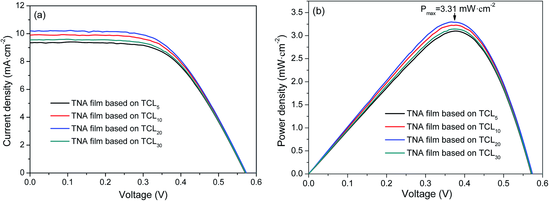 | ||
| Fig. 5 (a) I–V curves and (b) Pout curves of DSSCs grown over various TNA films with different TCLs. | ||
| TNA films grown over | Jsc (mA cm−2) | Voc (V) | FF (%) | PCE (%) |
|---|---|---|---|---|
| TCL5 | 9.3497 | 0.5711 | 58.08 | 3.10 |
| TCL10 | 9.8996 | 0.5731 | 56.90 | 3.23 |
| TCL20 | 10.2054 | 0.5737 | 56.30 | 3.30 |
| TCL30 | 9.5480 | 0.5716 | 57.59 | 3.14 |
Conclusions
This study provides a new method for the preparation of TCLs, which allows the preparation of TCLs more quickly, efficiently, simply and cheaply. The influence of TCL with different thickness on the performance of TNA films also provides a reference for further research. The innovative two-step method was used to prepare perfect TCLs with different thicknesses. Then, the TNA films were successfully grown over the TCLs. The results indicated that TCLs with appropriate thickness could effectively improve the morphology and photoelectric properties of TNA films. When compared with other TNA films grown over different TCLs, the one grown over TCL20 exhibited more ideal and comprehensive photoelectrochemical performance. The DSSC based on this TNA film achieved the highest Jsc (10.2054 mA cm−2), Voc (0.5737 V), PCE (3.3%) and Pout (3.31 mW cm−2).Conflicts of interest
There are no conflicts of interest to declare.Acknowledgements
This work was supported by the Chinese Postdoctoral Science Fund (2343/185179), the Chinese 02 Special Fund (2017ZX02408003), the Key Research Projects of Colleges and Universities in Henan Province (15A430023) and the Henan International Science and Technology Cooperation Programs (152102410035).References
- M. Saliba, T. Matsui, K. Domanski, J. Y. Seo, A. Ummadisingu, S. M. Zakeeruddin, J. P. C. Baena, W. R. Tress, A. Abate, A. Hagfeldt and M. Grätzel, Science, 2016, 354, 206–209 CrossRef CAS.
- Z. W. Xiao and Y. F. Yan, Adv. Energy Mater., 2017, 7, 1701136 CrossRef.
- C. Liang, P. W. Li, Y. Q. Zhang, H. Gu, Q. B. Cai, X. T. Liu, J. F. Wang, H. Wen and G. S. Shao, J. Power Sources, 2017, 372, 235–244 CrossRef CAS.
- I. Jeong, H. Jung, M. Park, J. S. Park, H. J. Son, J. Joo, J. Lee and M. J. Ko, Nano Energy, 2016, 28, 380–389 CrossRef CAS.
- Y. M. Xu, X. S. Li, M. Xiao and X. M. Xiong, CrystEngComm, 2018, 20, 6280–6290 RSC.
- Q. H. Liu, Q. Sun, M. Zhang, Y. Li, M. Zhao and L. F. Dong, Appl. Phys. A: Mater. Sci. Process., 2016, 122, 1–5 CAS.
- N. Irannejad, B. Rezaei, A. A. Ensafi and M. M. Momeni, Electrochim. Acta, 2017, 247, 764–770 CrossRef CAS.
- M. Asemi and M. Ghanaatshoar, J. Mater. Sci., 2017, 52, 489–503 CrossRef CAS.
- J. Du, Z. L. Du, J. S. Hu, Z. X. Pan, Q. Shen, J. K. Sun, D. H. Long, H. Dong, L. T. Sun, X. H. Zhong and L. J. Wan, J. Am. Chem. Soc., 2016, 138, 4201–4209 CrossRef CAS.
- M. X. Liu, O. Voznyy, R. Sabatini, F. P. García de Arquer, R. Munir, A. H. Balawi, X. Z. Lan, F. J. Fan, G. Walters, A. R. Kirmani, S. Hoogland, F. Laquai, A. Amassian and E. H. Sargent, Nat. Mater., 2017, 16, 258–263 CrossRef CAS.
- W. Wang, W. L. Feng, J. Du, W. N. Xue, L. L. Zhang, L. L. Zhao, Y. Li and X. H. Zhong, Adv. Mater., 2018, 1705746 CrossRef.
- E. M. Sanehira, A. R. Marshall, J. A. Christians, S. P. Harvey, P. N. Ciesielski, L. M. Wheeler, P. Schulz, L. Y. Lin, M. C. Beard and J. M. Luther, Sci. Adv., 2017, 3, eaao4204 CrossRef.
- W. Chen, M. Liu, Y. H. Wang, L. Gao, H. F. Dang and L. Q. Mao, Mater. Res. Bull., 2019, 116, 16–21 CrossRef CAS.
- L. Ge, Q. Hong, H. Li and F. Li, Chem. Commun., 2019, 55, 4945–4948 RSC.
- R. K. Sonker, S. Sikarwar, S. R. Sabhajeet, Rahul and B. C. Yadav, Opt. Mater., 2018, 83, 342–347 CrossRef CAS.
- P. Sanjay, K. Deepa, J. Madhavan and S. Senthil, Opt. Mater., 2018, 83, 192–199 CrossRef CAS.
- Y. F. Wang, Q. P. Luo, Y. Ding, X. Wang, X. F. Li and D. J. Li, Mater. Chem. Phys., 2018, 207, 141–146 CrossRef CAS.
- A. Ashok, S. N. Vijayaraghavan, G. E. Unni, S. V. Nair and M. Shanmugam, Nanotechnology, 2018, 29, 175401 CrossRef.
- Y. C. Chen, Y. C. Chang and C. M. Chen, J. Electrochem. Soc., 2018, 165, F409–F416 CrossRef CAS.
- A. Latini and R. Panetta, Energies, 2018, 11, 975 CrossRef.
- M. Amini, R. Keshavarzi, V. Mirkhani, M. Moghadam, S. Tangestaninejad, I. M. Baltork and F. Sadegh, J. Mater. Chem. A, 2018, 6, 2632–2642 RSC.
- J. A. Peñafiel-Castro, B. Hahn, R. L. Maltez, G. Knörnschild, P. Allonguec and L. F. P. Dick, Chem. Commun., 2018, 54, 3251–3254 RSC.
- P. Soundarrajan, K. Sankarasubramanian, K. Sethuraman and K. Ramamurthi, CrystEngComm, 2014, 16, 8756–8768 RSC.
- X. X. Wang, Y. D. Xiao, D. W. Zeng and C. S. Xie, CrystEngComm, 2015, 17, 1151–1158 RSC.
- Y. Y. Li, J. G. Wang, H. H. Sun and B. Q. Wei, ACS Appl. Mater. Interfaces, 2018, 10, 11580–11586 CrossRef CAS.
- P. Leidich, O. Linker, M. Panthöfer and W. Tremel, CrystEngComm, 2014, 16, 8486–8491 RSC.
- R. Sivakumar, J. Ramkumar, S. Shaji and M. Paulraj, Thin Solid Films, 2016, 615, 171–176 CrossRef CAS.
- R. Govindaraj, N. Santhosh, M. S. Pandian and P. Ramasamy, J. Cryst. Growth, 2017, 468, 125–128 CrossRef CAS.
- B. B. Çırak, S. M. Karadeniz, T. Kılınç, B. Caglar, A. E. Ekinci, H. Yelgin, M. Kürekçi and Ç. Çırak, Vacuum, 2017, 144, 183–189 CrossRef.
- N. Nyein, W. K. Tan, G. Kawamura, A. Matsuda and Z. Lockman, J. Photochem. Photobiol., A, 2017, 343, 33–39 CrossRef CAS.
- L. Q. Mao, Q. Q. Ba, S. Liu, X. J. Jia, H. Liu, W. Chen and X. Y. Li, RSC Adv., 2018, 8, 31529–31537 RSC.
- Y. L. Wan, M. M. Han, L. M. Yu, G. W. Yi and J. H. Jia, CrystEngComm, 2016, 18, 1577–1584 RSC.
- Q. Q. Gao, X. Y. Zhang, L. F. Duan, X. J. Li, X. S. Li, Y. Yang, Q. Yu and W. Lü, J. Alloys Compd., 2017, 715, 337–343 CrossRef CAS.
- S. S. Kim, S. I. Na and Y. C. Nah, Electrochim. Acta, 2011, 58, 503–509 CrossRef CAS.
- J. Liu, J. Huo, M. Zhang and X. D. Dong, Thin Solid Films, 2017, 623, 25–30 CrossRef CAS.
- S. M. Mokhtar, M. K. Ahmad, C. F. Soon, N. Nafarizal, A. B. Faridah, A. B. Suriani, M. H. Mamat, M. Shimomura and K. Murakami, Optik, 2018, 154, 510–515 CrossRef CAS.
- D. L. Jiang, Y. Q. Hao, R. J. Shen, S. Ghazarian, A. Ramos and F. M. Zhou, ACS Appl. Mater. Interfaces, 2013, 5, 11906–11912 CrossRef CAS.
- I. Jeong, Y. H. Park, S. Bae, M. Park, H. Jeong, P. Lee and M. J. Ko, ACS Appl. Mater. Interfaces, 2017, 9, 36865–36874 CrossRef CAS.
- J. Q. Qin, Z. L. Zhang, W. J. Shi, Y. F. Liu, H. P. Gao and Y. L. Mao, Nanoscale Res. Lett., 2017, 12, 640 CrossRef.
- R. L. Coppo, B. H. Farnum, B. D. Sherman, N. Y. M. Iha and T. J. Meyer, Sustainable Energy Fuels, 2017, 1, 112–118 RSC.
- J. J. Huang, C. K. Wu and C. F. Hsu, Appl. Phys. A, 2017, 123, 741 CrossRef.
- H. J. Liu, H. Bala, B. Zhang, B. B. Zong, L. W. Huang, W. Y. Fu, G. Sun, J. L. Cao and Z. Y. Zhan, J. Alloys Compd., 2018, 736, 87–92 CrossRef CAS.
- V. Manthina and A. G. Agrios, Thin Solid Films, 2016, 598, 54–59 CrossRef CAS.
- A. E. Shalan, S. Narra, T. Oshikiri, K. Ueno, X. Shi, H. P. Wu, M. M. Elshanawany, E. W. G. Diau and H. Misawa, Sustainable Energy Fuels, 2017, 1, 1533–1540 RSC.
- P. Lellig, M. A. Niedermeier, M. Rawolle, M. Meister, F. Laquai, P. M. Buschbaum and J. S. Gutmann, Phys. Chem. Chem. Phys., 2012, 14, 1607–1613 RSC.
- Tanvi, V. Saxena, A. Singh, O. Prakash, A. Mahajan, A. K. Debnath, K. P. Muthe and S. C. Gadkari, Sol. Energy Mater. Sol. Cells, 2017, 170, 127–136 CrossRef CAS.
- G. D. Rajmohan, F. Z. Huang, R. d'Agostino, J. d. Plessis and X. J. Dai, Thin Solid Films, 2017, 636, 307–313 CrossRef CAS.
- B. Liu and E. S. Aydil, J. Am. Chem. Soc., 2009, 131, 3985–3990 CrossRef CAS.
- Y. F. Deng, Z. H. Ma, F. Z. Ren, G. X. Wang and A. A. Volinsky, Chem. Phys. Lett., 2019, 724, 42–49 CrossRef CAS.
- W. L. Xu, H. Yuan, J. Xiao, C. Xiong and X. F. Zhu, Int. J. Mod. Phys. B, 2017, 31, 1744053 CrossRef CAS.
- P. Vivo, A. Ojanpera, J. H. Smått, S. Sanden, S. G. Hashmi, K. Kaunisto, P. Ihalainen, M. T. Masood, R. Osterbacka, P. D. Lund and H. Lemmetyinen, Org. Electron., 2017, 41, 287–293 CrossRef CAS.
- M. A. Alvi, A. A. Alghamdi and M. Zulfequar, J. Nanoelectron. Optoelectron., 2016, 11, 656–661 CrossRef CAS.
- D. T. Liu, S. B. Li, P. Zhang, Y. F. Wang, R. Zhang, H. Sarvari, F. Wang, J. Wu, Z. M. Wang and Z. D. Chen, Nano Energy, 2017, 31, 462–468 CrossRef CAS.
- J. B. Naceur, R. Ouertani, W. Chakhari and R. Chtourou, J. Mater. Sci.: Mater. Electron., 2019, 30, 5631–5639 CrossRef.
- A. W. Bott, Curr. Sep., 1998, 17(3), 87–91 CAS.
- X. Y. Niu, W. J. Yan, C. C. Shao, H. L. Zhao and J. K. Yang, Appl. Surf. Sci., 2019, 466, 882–892 CrossRef CAS.
- K. Chen, C. L. Chen, X. M. Ren, A. Alsaedi and T. Hayat, Chem. Eng. J., 2019, 359, 944–954 CrossRef CAS.
| This journal is © The Royal Society of Chemistry 2019 |