DOI:
10.1039/C9RA03721G
(Paper)
RSC Adv., 2019,
9, 19048-19056
Effect of Stone–Wales defects and transition-metal dopants on arsenene: a DFT study
Received
17th May 2019
, Accepted 13th June 2019
First published on 17th June 2019
Abstract
The structural, electronic, and magnetic properties of 3d transition metal (TM) atom (Sc, V, Cr, Mn, Co, and Cu) doped Stone–Wales (SW) defect arsenene were systematically investigated by density functional theory (DFT). The results indicated that the properties of arsenene were effectively changed by the SW-defect and TM-doping. Furthermore, chemical bonds formed between the TM-dopants and the adjacent As atoms of the SW-defect. The dopants Sc, Mn, and Cu induced an indirect-to-direct bandgap transition, and the doping of V, Cr, and Mn in SW-defect arsenene exhibited magnetic states. The magnetic moments of the systems depended on the number of spin-localized valence electrons. The functionalized electronic and magnetic properties of arsenene highlight the applications for electronics, optoelectronics, and spintronics.
1. Introduction
Two-dimensional (2D) materials with atomic thickness have witnessed a surge in research interest since graphene was fabricated by Geim et al.1–6 Among these, new group-VA 2D semiconducting materials, such phosphorene, arsenene, and antimonene, have attracted a great deal of attention because of their ultrathin nature and rather unique properties.7–15 Based on density functional theory (DFT) calculations it has been found that arsenic can form a single-layer structure, named arsenene.16,17 Recent investigations show that arsenene has an indirect band gap and extra high carrier mobility, which has potential in blue LED and photodetector applications.18 In experiments, the multilayer arsenene on InAs substrates has been successfully synthesized.19 In addition, defects are difficult to avoid during the preparation of 2D nanomaterials, which can also induce dramatic changes in the physical and chemical properties of materials. Furthermore, defects are formed by exposing materials to high energy irradiation of laser or electrons. Some typical point defects, such as adatoms, Stone–Wales (SW) defect and vacancies have been observed and investigated in 2D materials.20–26 Therefore, exploring the influence of defects on arsenene is meaningful for further potential applications of the arsenene material.
The arsenene is nonmagnetic, so the modifying of magnetism in arsenene is an interesting question. As we known, introducing of transition metal (TM) atoms in 2D materials has been demonstrated to be the most conventional and effective method to modify the magnetism.27–35 Furthermore, TM-doped 2D materials have been synthesized by pulsed laser deposition36 and electron beam irradiation.37–40 Some theoretical investigations have revealed that a magnetic state can be achieved by TM-doping. For instance, Zhou et al.15 investigated the influence of Co-doping arsenene, and the results indicated that magnetism of arsenene is tunable by the Co-doping and strain. Meanwhile, some theoretical studies explored the substitution of 3d-TM dopants in arsenene, which induced interesting magnetic and electronic behaviors.10,11,41 However, to the best of our knowledge, few investigations explored the effect of the coexistence of TM-doping and defects on arsenene.
In this paper, we aimed to clearly identify the influence of Stone–Wales defect and TM-doping (Sc, V, Cr, Co, and Cu) on the structural, electronic, and magnetic properties of arsenene. Also, we found that dopants of Sc, Mn and Cu tuned indirect band gap of arsenene to be direct. The results indicated that TM-doped arsenene had potential applications for spintronic devices.
2. Calculation details and models
Our results were obtained from first-principles plane-wave calculations based on density functional theory (DFT), as implemented in the Vienna Ab initio Simulation Package (VASP).42–44 The exchange-correlation potential was approximated by generalized gradient approximation (GGA) using Perdew–Burke–Ernzerhof (PBE) parameterization,45 and the Projector-Augmented Wave (PAW) pseudopotentials were used.46 A plane-wave basis set with the kinetic energy cutoff is 500 eV. The D3-Grimme correction (DFT-D3)47 has been set to account for London dispersion corrections. The convergence criterion between two consecutive steps was set as 10−6 eV and a maximum force of 0.001 eV Å−1 was allowed on each atom. The Brillouin zone had been sampled by 10 × 10 × 1 grid meshes in k-space by using Monkhorst–Pack scheme for 5 × 5 × 1 arsenene cells. Meanwhile, a vacuum space of 20 Å was introduced along the out-of-plane direction to avoid the interactions between the neighboring layers. To investigate the stability of Stone–Wales (SW) defect arsenene with dopants, the formation energy (Ef) for the doped structures, as follows:
| Ef = Edoped SW-As − ESW-As − (μTM − μAs) |
where Edoped SW-As represents the total energies of the doped SW-defect arsenene, and ESW-As is the total energy of SW-defect arsenene. Also, μTM (TM = Sc, V, Cr, Mn, Co, and Cu) and μAs are the chemical potentials.
3. Results and discussion
3.1 Pristine arsenene and vacancy-defect arsenene
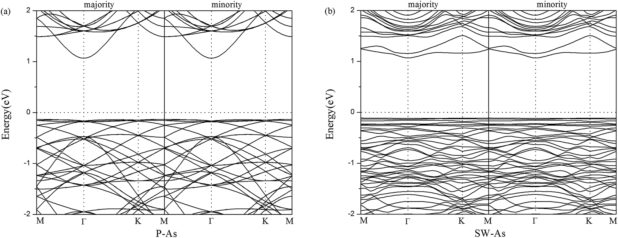
For the sake of comparison, we first performed the properties of perfect arsenene (P–As). The optimized atomic structure was showed in Fig. 1a. In our results, a buckle of 1.358 Å with the As–As bond length of 2.562 Å were obtained, which were well consistent with previous calculated data,10,15,37 indicating that our explored method was reliable. By rotating two adjacent As atoms for 90° in P–As, we obtained a SW-defect in arsenene and the SW-defect arsenene (SW-As) structure was also performed in Fig. 1b. Moreover, in order to examine the thermodynamic stability, we calculated the phonon vibration frequency of the As and SW-As structures, as shown in Fig. 1c and d. It can be seen that no imaginary phonon mode exists, indicating the dynamic stability of the two structures. To investigate the stability of SW-defect, we also calculated the formation energy of the defect, which was 1.65 eV and in agreement with previous studies.9,48 The electronic band structures were shown in Fig. 2. Form Fig. 2a it is obviously seen that P–As is indirect band gap semiconductor with a band gap of 1.30 eV. The valence band maximum (VBM) located at Γ-point, while the conduction band minimum (CBM) located at Γ–M direction. Interestingly, the presence of SW-defect increases the band gap in some sort, which is 1.41 eV and still is indirect band gap. The result may be caused by a small supercell and periodicity. But, additionally we note that, the VBM appears at Γ point, and the CBM appears at K point in SW-As structure.
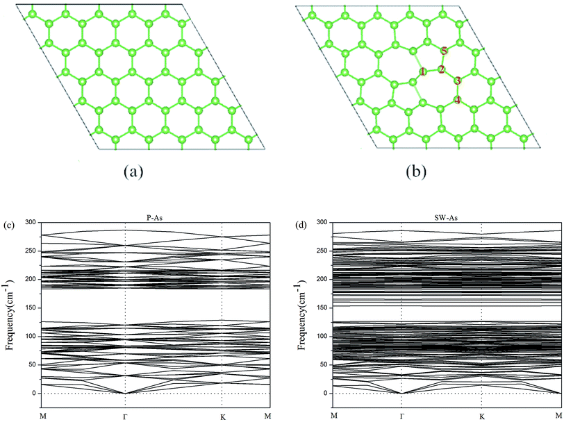 |
| | Fig. 1 The top view of the optimized geometric structures of (a) pristine arsenene and (b) Stone–Wales defect arsenene. The phonon band structure of (c) pristine arsenene and (d) Stone–Wales defect arsenene. | |
 |
| | Fig. 2 Band structures of (a) pristine arsenene and (b) Stone–Wales defect arsenene. | |
3.2 SW-defect arsenene with 3d-TM dopants
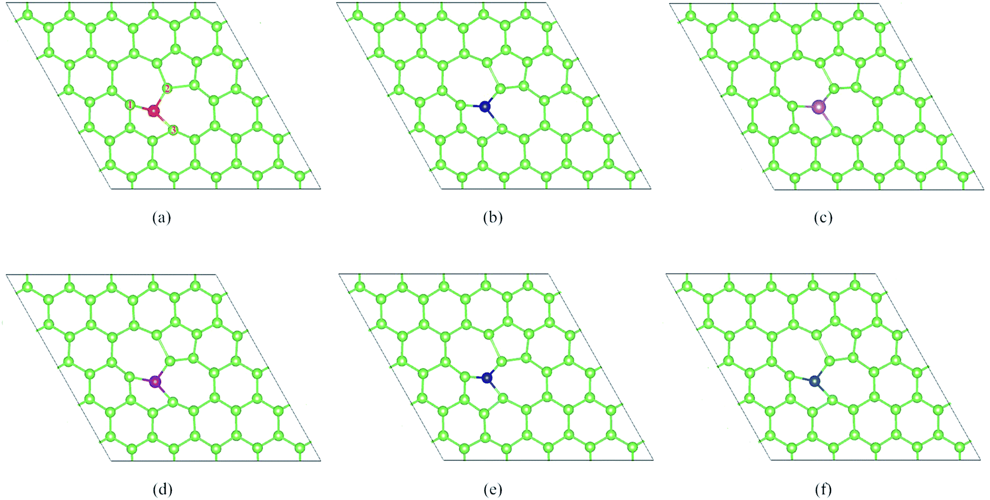
In this part, we consider the doping of 3d-TM atoms in SW-As structures. To explore the most stable doping systems, as labeled in Fig. 2b, we calculated five doping sites. The results indicate that the As5-site exhibits the lowest energy and then we substituted a 3d-TM atom into for As5 atom. The corresponding relaxed structures are shown in Fig. 3. It is found that all dopants formed covalent bond with three adjacent As atoms and we listed the bond lengths of As (1–3)-dopant (Fig. 3a) in Table 1. As summarized in Table 1, the bond lengths generally range from 2.23 Å to 2.72 Å. To investigate the stability of the SW-As with dopants, the formation energies (Ef) for all systems were also listed in Table 1. The most stability of the doped systems belongs to the most negative Ef value. As we can see, the Mn-dopant exhibit the largest formation energy with the value of −5.14 eV, while the smallest formation energy of −0.65 eV belong to Zn-dopant. Moreover, we analyzed the charge transfer of TM-dopants based on Bader charge population analysis.49 The results indicate that the charge transfer from TM-dopant to the As atoms, which implies that the SW-As system exhibited n-type feature. For example, in the structure of V/SW-As, the V lose charge of 0.89e and the adjacent As atoms (As1, As2, and As3) accept 0.32e, 0.24e, and 0.35e, respectively. The large charge transfer and small bond length suggested that chemical bonds formed between the TM-dopant and As atoms.
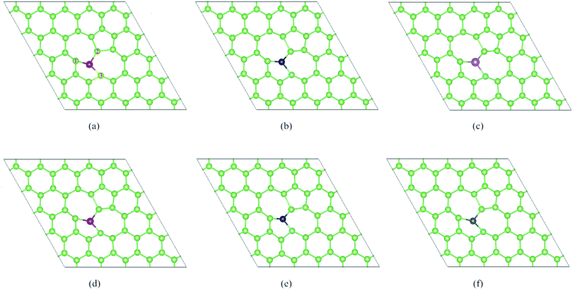 |
| | Fig. 3 The optimized doped structures of (a) Sc/SW-As, (b) V/SW-As, (c) Cr/SW-As, (d) Mn/SW-As, (e) Co/SW-As, (f) Cu/SW-As. | |
Table 1 Summary of results for transition-metal atoms doped SW-defect arsenene. The properties listed are the bond lengths of the TM-adatom to the adjacent As atoms of arsenene (d1, d2, and d3), the formations energy (Ef), and the charge transfer of TM-adatom (Q)
| Adatom |
d1 (Å) |
d2 (Å) |
d3 (Å) |
Ef (eV) |
Q (e) |
| Sc |
2.72 |
2.62 |
2.70 |
−2.93 |
0.51 |
| V |
2.61 |
2.35 |
2.44 |
−3.55 |
0.89 |
| Cr |
2.53 |
2.44 |
2.51 |
−4.51 |
0.73 |
| Mn |
2.53 |
2.43 |
2.53 |
−5.14 |
0.72 |
| Co |
2.32 |
2.23 |
2.30 |
−1.52 |
0.10 |
| Cu |
2.45 |
2.35 |
2.45 |
−0.65 |
0.17 |
3.3 Electronic and magnetic properties
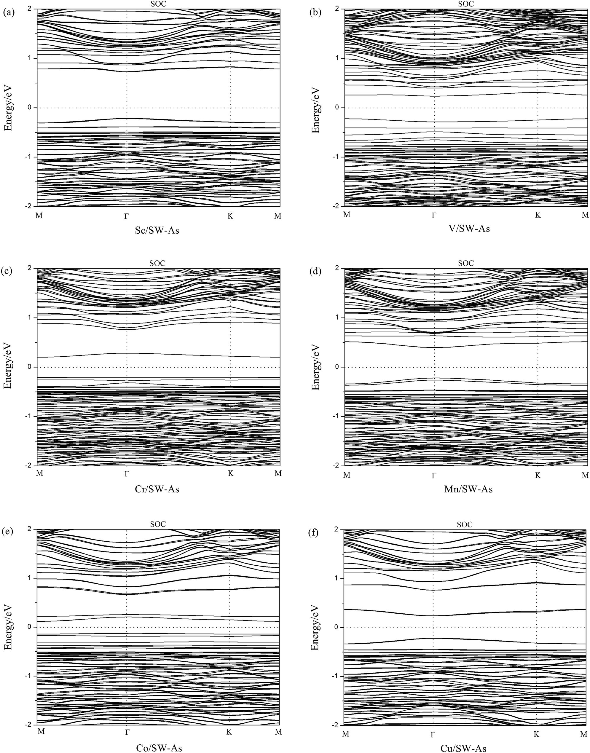
To get a better understanding of the influence of 3d-TM dopants on the electronic and magnetic properties of SW-defect arsenene, we performed the band structures of doped systems in Fig. 4. The spin-up channels (majority) and spin-down channels (minority) were listed separately. As we can see form the Fig. 4, the spin-up and spin-down bands are completely symmetric in Sc- and Cu-doped SW-As systems, which indicate the two systems were nonmagnetic. However, the both bands of the V-, Cr-, Mn-, and Co-doped systems are obviously asymmetric, which implies that the introducing of dopants changed the nonmagnetic state of SW-As. The magnetic properties depend on the different type of 3d-TM dopants. In order to analyze the electronic properties systemically, we summarized the results of band gaps and magnetic moments in Table 2. The band gaps of doped systems vary from 0.26 eV to 1.02 eV, which are semiconductors. It is found that the appearance of dopants decreased band gaps of SW-defect arsenene. Furthermore, the dopants of Sc, Mn, and Cu change the indirect band gap of SW-As structure into direct band gap. The valence band maximum and conduction band minimum both lie at Γ-point, while the other three systems still maintain indirect band gaps. Moreover, to examine the influence of SOC on splitting of the electronic bands of doped systems, we calculated the band structures with SOC and performed in Fig. 5. It can be found that the splitting of electronic bands is not obvious, and the shapes of band structures of the doped systems with and without SOC are similar, which is agreement with previous report.32
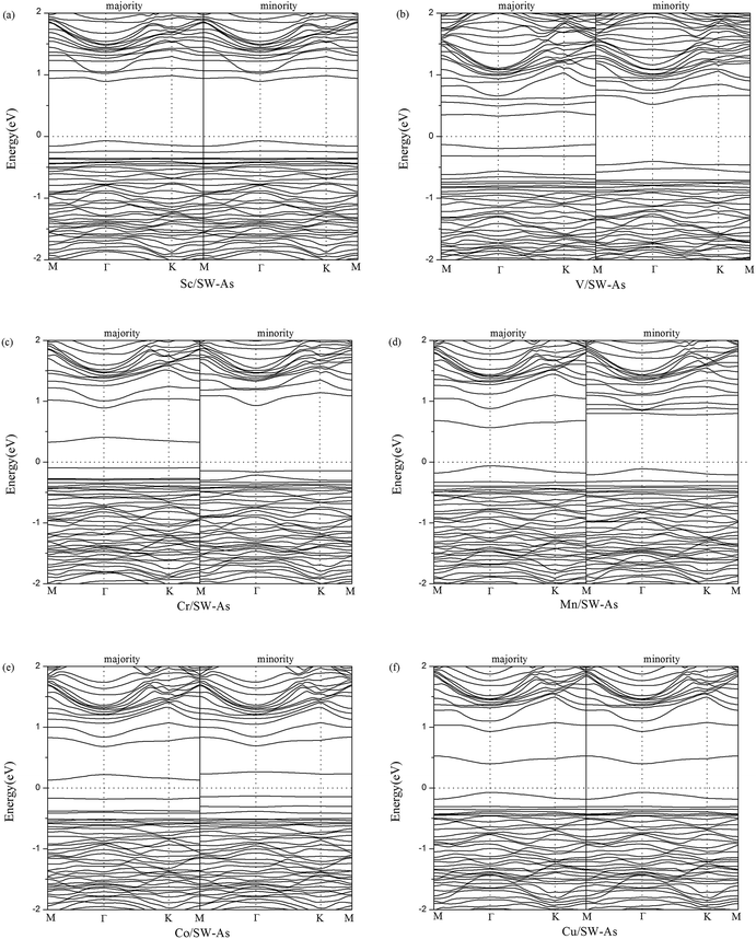 |
| | Fig. 4 Band structures of (a) Sc/SW-As, (b) V/SW-As, (c) Cr/SW-As, (d) Mn/SW-As, (e) Co/SW-As, (f) Cu/SW-As. | |
Table 2 The properties listed are the spin-up band gap (Eup-g), the spin-down band gap (Edown-g), the band gap (Eg), the magnetic moments of TM-adatoms (MTM), and the total magnetic moments of the adsorption systems (Mtotal)
| Adatom |
Eup-g (eV) |
Edown-g (eV) |
Eg (eV) |
MTM (μB) |
Mtotal (μB) |
| Sc |
0.96 |
0.96 |
0.96 |
0.0 |
0.0 |
| V |
0.46 |
0.93 |
0.46 |
2.2 |
2.0 |
| Cr |
1.11 |
1.10 |
1.02 |
3.4 |
3.0 |
| Mn |
0.63 |
0.89 |
0.63 |
3.7 |
4.0 |
| Co |
0.30 |
0.36 |
0.26 |
0.1 |
0.0 |
| Cu |
0.47 |
0.47 |
0.47 |
0.0 |
0.0 |
 |
| | Fig. 5 The band structures with SOC of (a) Sc/SW-As, (b) V/SW-As, (c) Cr/SW-As, (d) Mn/SW-As, (e) Co/SW-As, (f) Cu/SW-As. | |
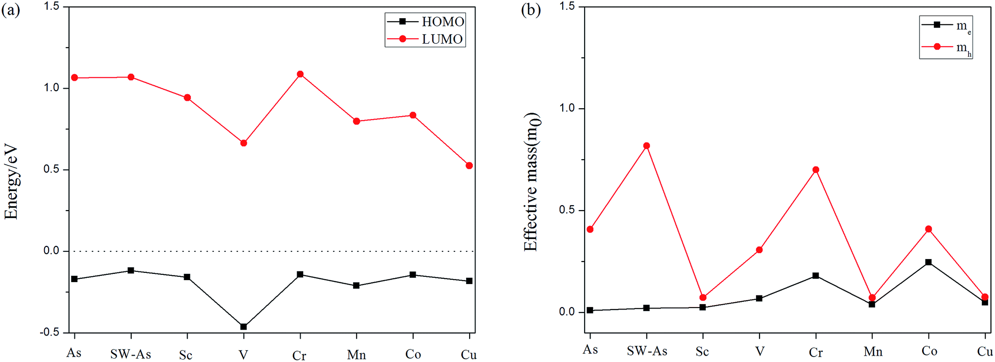
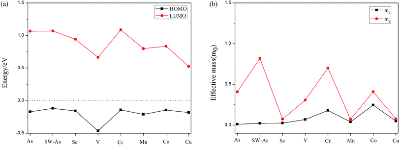
Furthermore, to deeply understand the effect of SW-defect and TM-dopant on the electronic properties, we calculated the HOMO (the highest occupied molecular orbital) and LUMO (the lowest occupied molecular orbital) levels of all structures, as shown in Fig. 6(a). Except for the V- and Cr-doped systems, the results of other systems indicate the presence of SW-defect and dopants decreases the LUMO level, while the HOMO level almost maintains the level of P–As. Therefore, it decreases the gaps of arsenene substrate. Moreover, we also calculated the effective mass of all systems25,29 and the results was performed in Fig. 6(b). For the doped systems, the dopant transfer charge to the As substrate, and then they are n-type semiconductor. It can be found that the effective mass of electrons in P–As and SW-As structures are 0.010m0 and 0.021m0. After the introducing of TM-dopants, the effective mass varied from 0.025m0 to 0.246m0, Except for the Cr- (0.180m0) and Co-doped (0.246m0) systems, the other structures still maintain high carrier mobility.
 |
| | Fig. 6 (a) HOMO and LUMO levels of the all structures, and the Fermi level is set to be zero. (b) The effective mass of the carrier as of all structures. | |
Previous studies indicated that the dopants of 3d-TM could enrich the magnetic properties of 2D materials, because of the isolated 3d-TM atoms exhibited various and obvious magnetic states. We also listed the magnetic moments of TM-dopants and the total magnetic moments of doped systems in Table 2. As shown in Table 2, the doping of V, Cr, and Mn change the nonmagnetic state of SW-defect arsenene to be magnetic, where the total magnetic moments (Mtotal) of systems depend on the types of dopants. The Mtotal of structures of V/SW-As, Cr/SW-As, and Mn/SW-As are 2.0 μB, 3.0 μB, and 4.0 μB, respectively. However, the Sc-, Co-, and Cu-doped SW-As systems are still nonmagnetic.
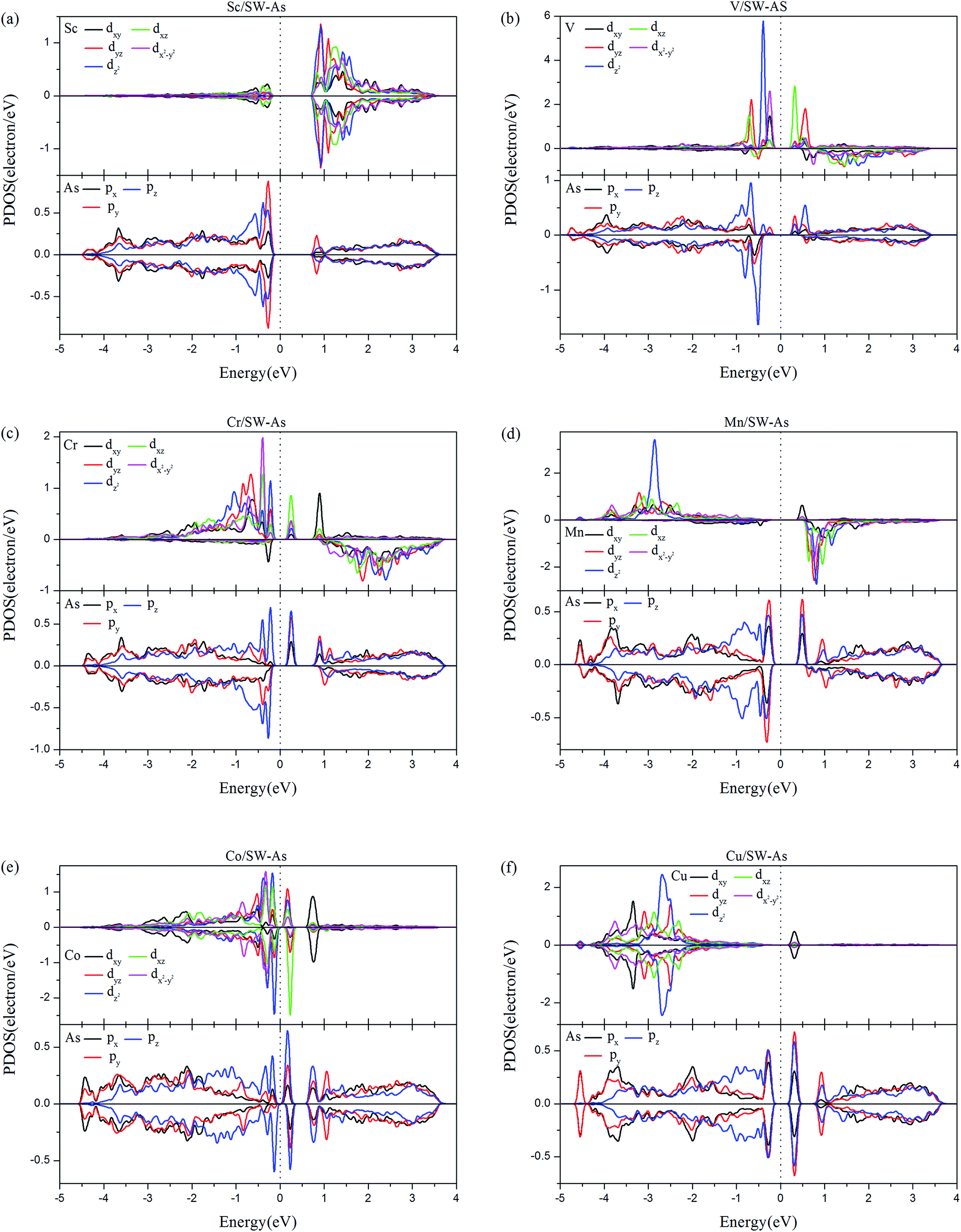
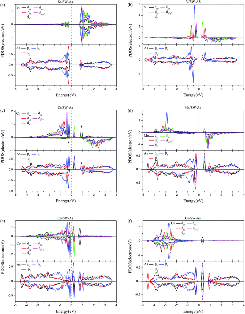
In order to deeply understand the contribution of different orbitals to the electronic and magnetic properties of doped systems, partial densities of states (PDOS) of TM-dopants and the adjacent As atoms (As1–As3) were carried out and shown in Fig. 7. From Fig. 7, we find that the spin-up and spin-down PDOS of Sc- and Cu-doped SW-defect arsenene are symmetric, which indicates nonmagnetic states and are agreement with the results listed in Table 2. In the system of V/SW-As, the magnetic properties are mainly contributed by dz2 orbital of V atom and pz orbital of As atoms near the Fermi level, which also exhibits a strong hybridization at about −0.50 eV. For the system of Cr-doped system, the spin-up channels of dxy, dx2–y2, and dz2 orbitals of Cr-dopant and pz orbital of As atoms dominated the magnetic property of Cr/SW-As. As for the system of Mn/SW-As, the magnetic state is resulted from asymmetric PDOS of Mn-dz2 orbital below the Fermi level and As-p orbital above the Fermi level. Meanwhile, as shown in Fig. 7, there is strong hybridization between the d-orbital of TM-dopants and p-orbital of As atoms, indicating that chemical bonds formed between the TM-atoms and adjacent As atoms.
 |
| | Fig. 7 The PDOS of the 3d-TM dopants and the As atoms (As1–As3) around the dopants: (a) Sc/SW-As, (b) V/SW-As, (c) Cr/SW-As, (d) Mn/SW-As, (e) Co/SW-As, (f) Cu/SW-As. | |
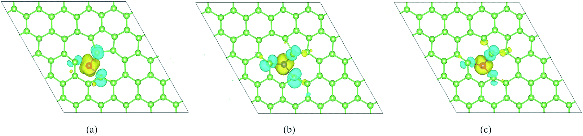
Finally, to further investigate the magnetic moment distribution of doped SW-defect arsenene, we drew spin density of magnetic systems in Fig. 8. It is found that spin-up density was obviously localized at TM-dopants (V, Cr, and Mn), while the spin-down density are contributed by adjacent As atoms around the SW-defect. Furthermore, the spectral shapes of spin density are similar, which originates from the similar distribution of spin-polarized valence electrons. Based on the analysis of magnetic properties, it is worth to expect assess these localized moments in experiments.
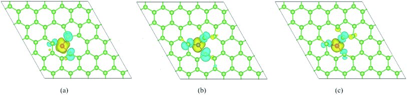 |
| | Fig. 8 Top view of calculated spin density of TM-adatoms doped SW-defect arsenene: (a) V/SW-As, (b) Cr/SW-As, and (c) Mn/SW-As. The isosurface value are set to be 0.002 e Å−1. | |
4. Conclusions
In conclusion, we predicted the influence of Stone–Wales defect and 3d-TM dopants (Sc, V, Cr, Mn, Co, and Cu) on the electronic and magnetic properties based on DFT calculations. The introducing of SW-defect enlarged the indirect band gap of arsenene, while SW-As system still exhibited semiconductor. After doping TM-atoms, nonmagnetic semiconductor nature of SW-As became narrow gap semiconductor character and showed different magnetic states. The total magnetic moments of three systems (V/SW-As, Cr/SW-As, and Mn/SW-As) increased depending on the increasing numbers of spin-localized valence electrons of TM-dopants. Briefly, we believe that fictionalization of arsenene through SW-defect and 3d-TM atoms is relevant for the application of arsenene.
Conflicts of interest
There are no conflicts to declare.
Acknowledgements
This work is supported by Student Research Training Program of School of Physics and Engineering (Grant No. 201917), and National Natural Science Foundation of China (NSFC, Grant No. 11604080 and 61874160).
References
- K. S. Novoselov, A. K. Geim, S. V. Morozov, D. Jiang, Y. Zhang, S. V. Dubonos, I. V. Grigorieva and A. A. Firsov, Electric Field Effect in Atomically Thin Carbon Films, Science, 2004, 306, 666 CrossRef CAS PubMed.
- A. K. Geim and K. S. Novoselov, The rise of graphene, Nat. Mater., 2007, 6, 183 CrossRef CAS PubMed.
- M. A. Rafiee, Graphene-based Composite Materials, Nature, 2006, 442, 282 CrossRef PubMed.
- H. Zhang, Y. Ma and Z. Chen, Quantum spin hall insulators in strain-modified arsenene, Nanoscale, 2015, 7, 19152–19159 RSC.
- Z. Xiaolong and B. I. Yakobson, An open canvas-2D materials with defects, disorder, and functionality, Acc. Chem. Res., 2015, 48, 73–80 CrossRef PubMed.
- X. Sui, C. Si, B. Shao, X. Zou, J. Wu, B. L. Gu and W. Duan, Tunable Magnetism in Transition Metal Decorated Phosphorene, J. Phys. Chem. C, 2015, 119, 10059–10063 CrossRef CAS.
- Z. Yungang and L. Xudong, Effects of interstitial dopings of 3d transition metal atoms on antimonene: A first-principles study, Appl. Surf. Sci., 2018, 458, 572–579 CrossRef.
- A. A. Kistanov, Y. Cai, D. R. Kripalani, K. Zhou, S. V. Dmitriev and Y.-W. Zhang, A first-principles study on the adsorption of small molecules on antimonene: oxidation tendency and stability, J. Mater. Chem. C, 2018, 6, 4308–4317 RSC.
- X. Liang, S.-P. Ng, N. Ding and C.-M. L. Wu, Characterization of point defects in monolayer arsenene, Appl. Surf. Sci., 2018, 443, 74–82 CrossRef CAS.
- M. Y. Liu, Q. Y. Chen, Y. Huang, Z. Y. Li, C. Cao and Y. He, Electronic and magnetic properties of 3D transition-metal atom adsorbed arsenene, Nanotechnology, 2018, 29, 095203 CrossRef PubMed.
- M. Y. Liu, Y. Huang, Q. Y. Chen, C. Cao and Y. He, Unexpected electronic structure of the alloyed and doped arsenene sheets: First-Principles calculations, Sci. Rep., 2016, 6, 29114 CrossRef CAS PubMed.
- Z. H. Benam, H. Arkin and E. Aktürk, Point defects in buckled and asymmetric washboard phases of arsenic phosphorus: A first principles study, Comput. Mater. Sci., 2017, 140, 290–298 CrossRef CAS.
- P. Liu, Y. Z. Nie, Q. L. Xia and G. H. Guo, Structural and electronic properties of arsenic nitrogen monolayer, Phys. Lett. A, 2017, 381, 1102–1106 CrossRef CAS.
- O. Üzengi Aktürk, E. Aktürk and S. Ciraci, Effects of adatoms and physisorbed molecules on the physical properties of antimonene, Phys. Rev. B, 2016, 9, 035450 CrossRef.
- Y. Zhou, G. Cheng and J. Li, Coexistence of Co doping and strain on arsenene and antimonene: tunable magnetism and half-metallic behavior, RSC Adv., 2018, 8, 1320–1327 RSC.
- Z. Shengli, Y. Zhong, L. Yafei, C. Zhongfang and Z. Haibo, Atomically thin arsenene and antimonene: semimetal-semiconductor and indirect-direct band-gap transitions, Angew. Chem., 2015, 127, 3155–3158 CrossRef.
- J. Zhao, C. Liu, W. Guo and J. Ma, Prediction on the light-assisted exfoliation of multilayered arsenene by the photo-isomerization of azobenzene, Nanoscale, 2017, 9, 7006–7011 RSC.
- S. Zhang, Z. Yan, Y. Li, Z. Chen and H. Zeng, Atomically Thin Arsenene and Antimonene: Semimetal–Semiconductor and Indirect–Direct Band-Gap Transitions, Angew. Chem., Int. Ed., 2015, 54, 3112–3115 CrossRef CAS PubMed.
- H. S. Tsai, S. W. Wang, C. H. Hsiao, C. W. Chen, H. Ouyang, Y. L. Chueh, H. C. Kuo and J. H. Liang, Direct Synthesis and Practical Bandgap Estimation of Multilayer Arsenene Nanoribbons, Chem. Mater., 2016, 28, 425–429 CrossRef CAS.
- A. R. Rocha, T. B. Martins, A. Fazzio and A. N. J. R. Silva, Da, Disorder-based graphene spintronics, Nanotechnology, 2010, 21, 345202 CrossRef CAS PubMed.
- T. T. Li, C. He and W. X. Zhang, A novel porous C4N4 monolayer as a potential anchoring material for lithium–sulfur battery design, J. Mater. Chem. A, 2019, 7, 4134–4144 RSC.
- C. Xu, G. Luo, Q. Liu, J. Zheng, Z. Zhang, S. Nagase, Z. Gao and J. Lu, Giant magnetoresistance in silicene nanoribbons, Nanoscale, 2012, 4, 3111–3117 RSC.
- Z. Ni, H. Zhong, X. Jiang, R. Quhe, G. Luo, Y. Wang, M. Ye, J. Yang, J. Shi and J. Lu, Tunable band gap and doping type in silicene by surface adsorption: towards tunneling transistors, Nanoscale, 2014, 6, 7609–7618 RSC.
- F. Banhart, J. Kotakoski and A. V. Krasheninnikov, Structural defects in graphene, ACS Nano, 2011, 5, 26–41 CrossRef CAS PubMed.
- M. M. Dong, C. He and W. X. Zhang, Tunable and sizable bandgap of g-C3N4/graphene/g-C3N4 sandwich heterostructure: a van der Waals density functional study, J. Mater. Chem. C, 2017, 5, 3830–3837 RSC.
- P. Xiangyang and A. Rajeev, Symmetry breaking induced bandgap in epitaxial graphene layers on SiC, Nano Lett., 2008, 8, 4464–4468 CrossRef PubMed.
- A. V. Krasheninnikov, P. O. Lehtinen, A. S. Foster, P. Pyykk and R. M. Nieminen, Embedding transition-metal atoms in graphene: structure, bonding, and magnetism, Phys. Rev. Lett., 2009, 102, 126807 CrossRef CAS PubMed.
- H. Bing, X. Hongjun, Y. Jaejun and W. Su-Huai, Effective control of the charge and magnetic states of transition-metal atoms on single-layer boron nitride, Phys. Rev. Lett., 2012, 108, 206802 CrossRef.
- C. He, G. Liu, W. X. Zhang, Z. Q. Shi and S. L. Zhou, Tuning the structures and electron transport properties of ultrathin Cu nanowires by size and bending stress using DFT and DFTB methods, RSC Adv., 2015, 5, 22463–22470 RSC.
- D. Ma, W. Ju, T. Li, X. Zhang, C. He, B. Ma, Y. Tang, Z. Lu and Z. Yang, Modulating electronic, magnetic and chemical properties of MoS2 monolayer sheets by substitutional doping with transition metals, Appl. Surf. Sci., 2016, 364, 181–189 CrossRef CAS.
- L. Wang, H. Qiu, C. B. Liang, P. Song, J. W. Gu and Z. H. Guo, Electromagnetic Interference Shielding MWCNT-Fe3O4@Ag/Epoxy Nanocomposites with Satisfactory Thermal Conductivity and High Thermal Stability, Carbon, 2019, 141, 506–514 CrossRef CAS.
- C. He, M. Cheng and W. X. Zhang, Tunable electronic and magnetic properties of transition metals doped antimonene: a first-principles study, Mater. Res. Express, 2018, 5, 065059 CrossRef.
- Y. M. Huangfu, C. B. Liang, Y. X. Han, L. Wang, J. Kong and J. W. Gu, Fabrication and investigation on the Fe3O4/thermally annealed graphene aerogel/epoxy electromagnetic interference shielding nanocomposites, Compos. Sci. Technol., 2019, 169, 70–75 CrossRef CAS.
- X. Q. Wang, W. G. Chen, Z. L. Zhu and Y. Jia, Electronic and Magnetic Properties Modulated by Adsorption of 3d Transition Metal Atoms in Monolayer and Bilayer MoS2 Sheets, Acta Metall. Sin. (Engl. Lett.), 2015, 28, 793–798 CrossRef CAS.
- L. Yang, S. Yan, W. Mi and X. Wang, Prediction of Spin-Dependent Electronic Structure in 3d-Transition-Metal Doped Antimonene, Appl. Phys. Lett., 2016, 109, 173–1669 Search PubMed.
- H. Wang, Q. Wang, Y. Cheng, K. Li, Y. Yao, Q. Zhang, C. Dong, P. Wang, U. Schwingenschlögl and W. Yang, Doping monolayer graphene with single atom substitutions, Nano Lett., 2012, 12, 141–144 CrossRef CAS PubMed.
- J. A. Rodríguez-Manzo, C. Ovidiu and B. Florian, Trapping of metal atoms in vacancies of carbon nanotubes and graphene, ACS Nano, 2010, 4, 3422–3428 CrossRef PubMed.
- A. W. Robertson, B. Montanari, K. He, J. Kim, C. S. Allen, Y. A. Wu, J. Olivier, J. Neethling, N. Harrison and A. I. Kirkland, Dynamics of single Fe atoms in graphene vacancies, Nano Lett., 2013, 13, 1468–1475 CrossRef CAS PubMed.
- Z. He, K. He, A. W. Robertson, A. I. Kirkland, D. Kim, J. Ihm, E. Yoon, G. D. Lee and J. H. Warner, Atomic Structure and Dynamics of Metal Dopant Pairs in Graphene, Nano Lett., 2014, 14, 3766–3772 CrossRef CAS PubMed.
- L. Yung-Chang, D. O. Dumcenco, K. Hannu-Pekka, N. Yoshiko, A. V. Krasheninnikov, H. Ying-Sheng and S. Kazu, Properties of individual dopant atoms in single-layer MoS2: atomic structure, migration, and enhanced reactivity, Adv. Mater., 2014, 26, 2857–2861 CrossRef PubMed.
- M. Sun, S. Wang, Y. Du, Y. Jin and W. Tang, Transition metal doped arsenene: A first-principles study, Appl. Surf. Sci., 2016, 389, 594–600 CrossRef CAS.
- G. Kresse, Ab initio molecular dynamics for liquid metals, Phys. Rev. B: Condens. Matter Mater. Phys., 1993, 48, 13115–13118 CrossRef CAS PubMed.
- G. Kresse and J. Furthmüller, Efficiency of ab-initio total energy calculations for metals and semiconductors using a plane-wave basis set, Comput. Mater. Sci., 1996, 6, 15–50 CrossRef CAS.
- G. Kresse and J. Furthmüller, Efficient iterative schemes for ab initio total-energy calculations using a plane-wave basis set, Phys. Rev. B: Condens. Matter Mater. Phys., 1996, 54, 11169–11186 CrossRef CAS PubMed.
- J. P. Perdew, K. Burke and M. Ernzerhof, Generalized Gradient Approximation Made Simple, Phys. Rev. Lett., 1996, 77, 3865–3868 CrossRef CAS PubMed.
- G. Kresse and D. Joubert, From ultrasoft pseudopotentials to the projector augmented-wave method, Phys. Rev. B: Condens. Matter Mater. Phys., 1999, 59, 1758–1775 CrossRef CAS.
- G. Stefan, Semiempirical GGA-type density functional constructed with a long-range dispersion correction, J. Comput. Chem., 2010, 27, 1787–1799 Search PubMed.
- X. Sun, Y. Liu, Z. Song, Y. Li, W. Wang, H. Lin, L. Wang and Y. Li, Structures, mobility and electronic properties of point defects in arsenene, antimonene and an antimony arsenide alloy, J. Mater. Chem. C, 2017, 5, 4159–4166 RSC.
- W. Tang, E. Sanville and G. Henkelman, A grid-based Bader analysis algorithm without lattice bias, J. Phys.: Condens. Matter, 2009, 21, 084204 CrossRef CAS.
|
| This journal is © The Royal Society of Chemistry 2019 |
Click here to see how this site uses Cookies. View our privacy policy here. 
 Open Access Article
 This Open Access Article is licensed under a Creative Commons Attribution-Non Commercial 3.0 Unported Licence
 *ab,
Weiwei Jua,
Qian Zhanga and
Yanling Liua
*ab,
Weiwei Jua,
Qian Zhanga and
Yanling Liua