
 Open Access Article
 This Open Access Article is licensed under a Creative Commons Attribution-Non Commercial 3.0 Unported Licence
A comprehensive optical analysis of nanoscale structures: from thin films to asymmetric nanocavities†
Giuseppe Emanuele Lio *,
Giovanna Palermo,
Roberto Caputo and
Antonio De Luca*
*,
Giovanna Palermo,
Roberto Caputo and
Antonio De Luca*
CNR-Nanotec, Cosenza and Physics Department, University of Calabria, 87036 Arcavacata di Rende, CS, Italy. E-mail: giuseppe.lio@unical.it; antonio.deluca@unical.it
First published on 11th July 2019
Abstract
A simple and robust method able to evaluate and predict, with high accuracy, the optical properties of single and multi-layer nanostructures is presented. The method was implemented using a COMSOL Multiphysics simulation platform and it has been validated by four case studies with increasing numerical complexities: (i) a single thin layer (20 nm) of Ag deposited on a glass substrate; (ii) a metamaterial composed of five bi-layers of Ag/ITO (indium tin oxide), with a thickness of 20 nm each; (iii) a system based on a three-material unit cell (AZO/ITO/Ag), but without any thickness periodicity (AZO stands for Al2O3/zinc oxide); (iv) an asymmetric nanocavity (thin-ITO/Ag/thick-ITO/Ag). A thorough study of this latter configuration reveals peculiar metamaterial effects that can widen the actual scenario in nanophotonic applications. Numerical results have been compared with experimental data provided by real ellipsometric measurements performed on the above mentioned ad hoc fabricated nanostructures. The obtained agreement is excellent, suggesting this research as a valid design approach to realize multi-band metamaterials able to work in a broad spectral range.
1 Introduction
In the last few years, the complexity of systems focused on materials science and experimental physics is gradually increasing to the point that analytical approaches to theoretical modeling are being overshadowed in the field by their numerical counterparts. This trend in research is thus promoting the evolution of comprehensive numerical packages that provide extremely accurate descriptions of physical processes.1–3 Handily, commercial packages now provide highly reliable modeling of phenomena like structural or fluid behaviors,4–7 wave propagation,8–13 and thermal transport,14–16 to name but a few. As a consequence, the availability of such powerful tools is modifying the way research is performed, eventually suggesting new possibilities to optimize the scientific procedure itself. Within the portfolio of experimental characterization techniques, it is remarkable what detailed insight can be acquired when performing spectroscopic ellipsometry of thin films and bulk materials,17–19 including the monitoring of film growth,20 surface roughness,21 detection of micro- and nano-structures on a surface,22–24 and determination of general optical material characteristics.25–28 Indeed, after design and realization of a specific system, ellipsometric characterization typically represents a crucial test-bed, providing a validation of the expected functionalities or helpful hints for improvement. At this stage, a trial-and-error procedure to achieve the desired target very often results in numerous attempts. Considering the vast range of applicability of ellipsometry, the possibility of implementing this technique as a reliable numerical method, able to a priori predict the result of the real experimental analysis before actually performing it, is evidently extremely convenient. This is especially true when the focus of the study is a complex nanostructured system whose fabrication can be largely time-consuming and expensive.In literature, preliminary attempts at implementing a numerical ellipsometric analysis by means of finite element method (FEM) simulations in different spectral ranges have been reported,29–33 mainly proposing an ideal starting point such as solution of single layer materials with functionalities in the VIS-NIR range. However, the approach in these cases is limited to a scattered field study instead of a full field analysis.
Here, we present a novel method, implemented using the COMSOL Multiphysics FEM commercial platform,34 providing a comprehensive ellipsometric analysis of general multi-layer systems with extreme freedom of design in terms of thickness, composition and number of layers. For each considered system, the proposed numerical ellipsometric analysis (NEA) allows for the calculation of the main physical quantities of interest for different polarizations and angles of incidence.
2 The numerical simulation environment
In the simulation geometry presented in this work (Fig. 1a), an electromagnetic plane wave (E(![[r with combining macron]](https://www.rsc.org/images/entities/i_char_0072_0304.gif) ,t) = E0
,t) = E0![[thin space (1/6-em)]](https://www.rsc.org/images/entities/char_2009.gif) exp[i(
exp[i(![[k with combining macron]](https://www.rsc.org/images/entities/i_char_006b_0304.gif) · − ωt + ϕ)]) impinges on a generic multi-layer system from the superstrate (typically air), with a specific incident angle and polarization (s-polarization (TE) or p-polarization (TM)). Light interacting with the structure is then collected through both its substrate (typically glass) and superstrate, permitting us to compute the optical quantities of interest (transmittance (T), reflectance (R), the Brewster angle, field maps and so on). This is done by solving the frequency-domain partial differential equation (PDE) that governs the E and H fields associated with the electromagnetic wave propagating through the structure:
· − ωt + ϕ)]) impinges on a generic multi-layer system from the superstrate (typically air), with a specific incident angle and polarization (s-polarization (TE) or p-polarization (TM)). Light interacting with the structure is then collected through both its substrate (typically glass) and superstrate, permitting us to compute the optical quantities of interest (transmittance (T), reflectance (R), the Brewster angle, field maps and so on). This is done by solving the frequency-domain partial differential equation (PDE) that governs the E and H fields associated with the electromagnetic wave propagating through the structure:| ∇ × μr−1(∇ × E) − ω2ε0μ0(εr − iσ/ωε0)E = 0 | (1) |
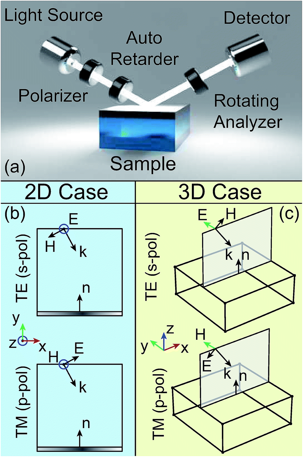 | ||
| Fig. 1 (a) Pictorial view of a basic ellipsometer setup. The sample is a thin film on a glass substrate. The sketches of the electric and magnetic field components for s- and p-polarized light impinging on the sample are depicted in the case of a 2D (b) and a 3D (c) numerical simulation. | ||
With the conditions of the electric conductivity σ = 0 and non-magnetic materials (μr = 1), the previous equation reduces to:
| ∇ × (∇ × E) − k02εrE = 0 | (2) |
![[r with combining tilde]](https://www.rsc.org/images/entities/i_char_0072_0303.gif) p/s, where p and s are the complex Fresnel coefficients related to the square roots of the reflectances for the two different polarizations,
p/s, where p and s are the complex Fresnel coefficients related to the square roots of the reflectances for the two different polarizations,  and
and  . Asρ is a complex quantity, it can also be written as tan(Ψ)eiΔ. Thus, tan(Ψ) is related to the amplitude ratio upon reflection (Ψ = arctan(rp/rs)), whereas Δ represents the phase shift between the two components (Δ = ϕp − ϕs).33,35 Since ellipsometry measures the ratio (or difference) of two values (rather than their absolute values), it is very robust, accurate and reproducible.
In order to simulate the behaviors of TE (s-pol) and TM (p-pol) polarized light36 in a 2D environment, it is necessary to properly write the components of the electromagnetic fields with respect to the incidence plane (xy). To select the s-polarization in COMSOL, an “out of plane” configuration has to be used (E = (0, 0, 1)), while to select the p-polarization, the user has to apply the “in plane wave-vector” scheme; in this case the magnetic field has to be used as H = (0, 0, 1). In a 3D simulation, the incident plane corresponds to the xz plane and the polarizations are set accordingly: E = (0, 1, 0) for s-pol or H = (0, 1, 0) for p-pol. The four sketches shown in Fig. 1b and c clarify how to set the field components in COMSOL.
To optimize the computation time of the NEA calculation, Floquet periodic boundary conditions (PBCs) were set to all boundaries. The PBCs ensure the simulation of systems with infinite size along the selected directions (ESI, Fig. S1†). Another way to optimize the computation process consists of parallelizing the solvers by introducing two “frequency domain studies”, able to solve eqn (2) for both s- and p-polarized light.
The discretization of the problem was realized through the choice of a dense mesh weave, ensuring that the numerical simulation takes into account the size of the real layers (sub-nanometric sizes are not considered to avoid unphysical results, Fig. S1c†).
3 Results and discussion
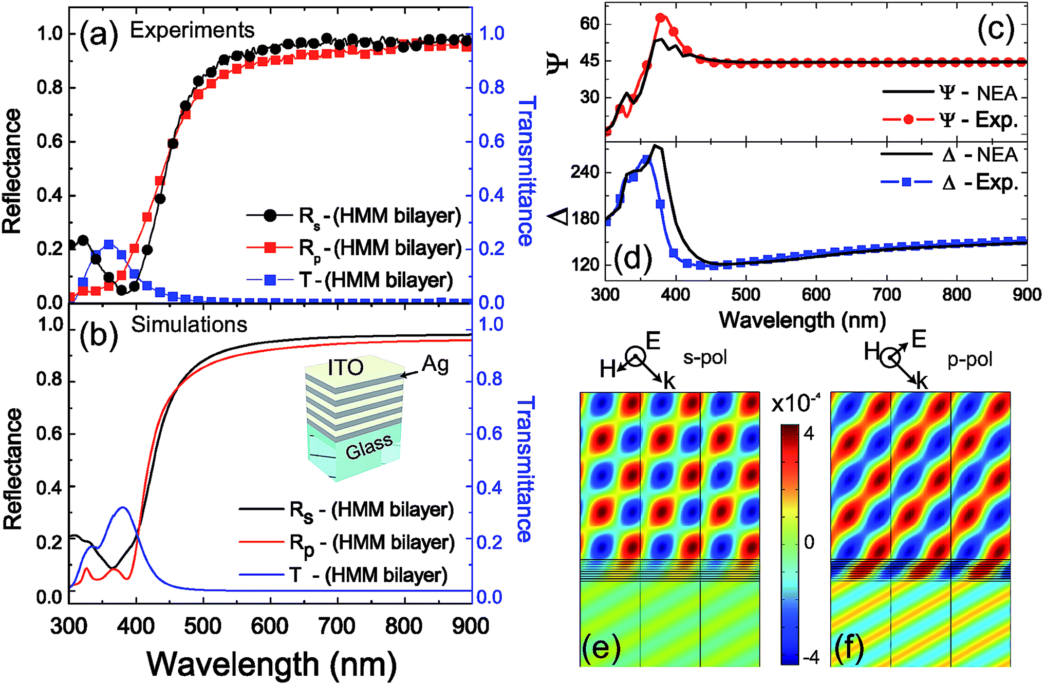
In order to validate the effectiveness of the NEA modeling, numerical predictions were compared with the results of measurements performed on corresponding real samples. Several multi-layer systems have been designed, fabricated and characterized using experimental ellipsometric analysis. The first and simplest system was a single Ag layer deposited on a glass substrate (20 nm thickness). The following system was a hyperbolic metamaterial37 made of a stack of five alternated Ag/ITO bi-layers (ITO stands for indium tin oxide) with the single bilayer having a thickness of 40 nm (20/20). The third system was characterized by a three-materials unit cell repeated three times. The unit cell was made of Al2O3 doped zinc oxide (AZO), ITO and Ag. The numerical task was particularly difficult because each of the three cells that were the constituents of the system had different thicknesses for each layer. The last and most complex system comprised an asymmetric optical cavity, with nanoscale features, also known as metal–insulator–metal (MIM).38,39 Starting from the glass substrate, this system was composed of an Ag layer covered by a thick ITO slab, representing the dielectric cavity, and an Ag/thin-ITO bilayer on top. All samples were experimentally fabricated by exploiting a DC sputtering technique. Then, for all cases, the experimental reflectance, transmittance and ellipsometric angles Ψ and Δ were measured by means of a M-2000 ellipsometer (J.A. Woollam).Fig. 2a and b respectively show the directly measured reflectance and transmittance, as well as the corresponding numerical curves provided by the NEA simulation for the first case study. The reflectances, Rp and Rs curves, were measured and calculated by considering an incident angle of θi = 50°, while the transmittance was measured and simulated at normal incidence. The minimum value at about 350 nm in the reflectance curves (and the related maximum in the transmittance ones) is referred to as the Ferrell–Berreman mode for a silver nanometric layer.40 The difference of about 20% between the amplitude of the experimental and simulated curves is due to the presence of the glass substrate in the real sample, that is partially considered in the simulated case. Indeed, in order to optimize the computational time, the size of the glass in the simulation was decreased to 1200 nm instead of the real 1.1 mm. The results are different only in absolute values but not in the general trends of the curves. Apart from that, the agreement between measurements and simulations is quite satisfactory. Fig. 2c and d show the Ψ and Δ behaviors, respectively.
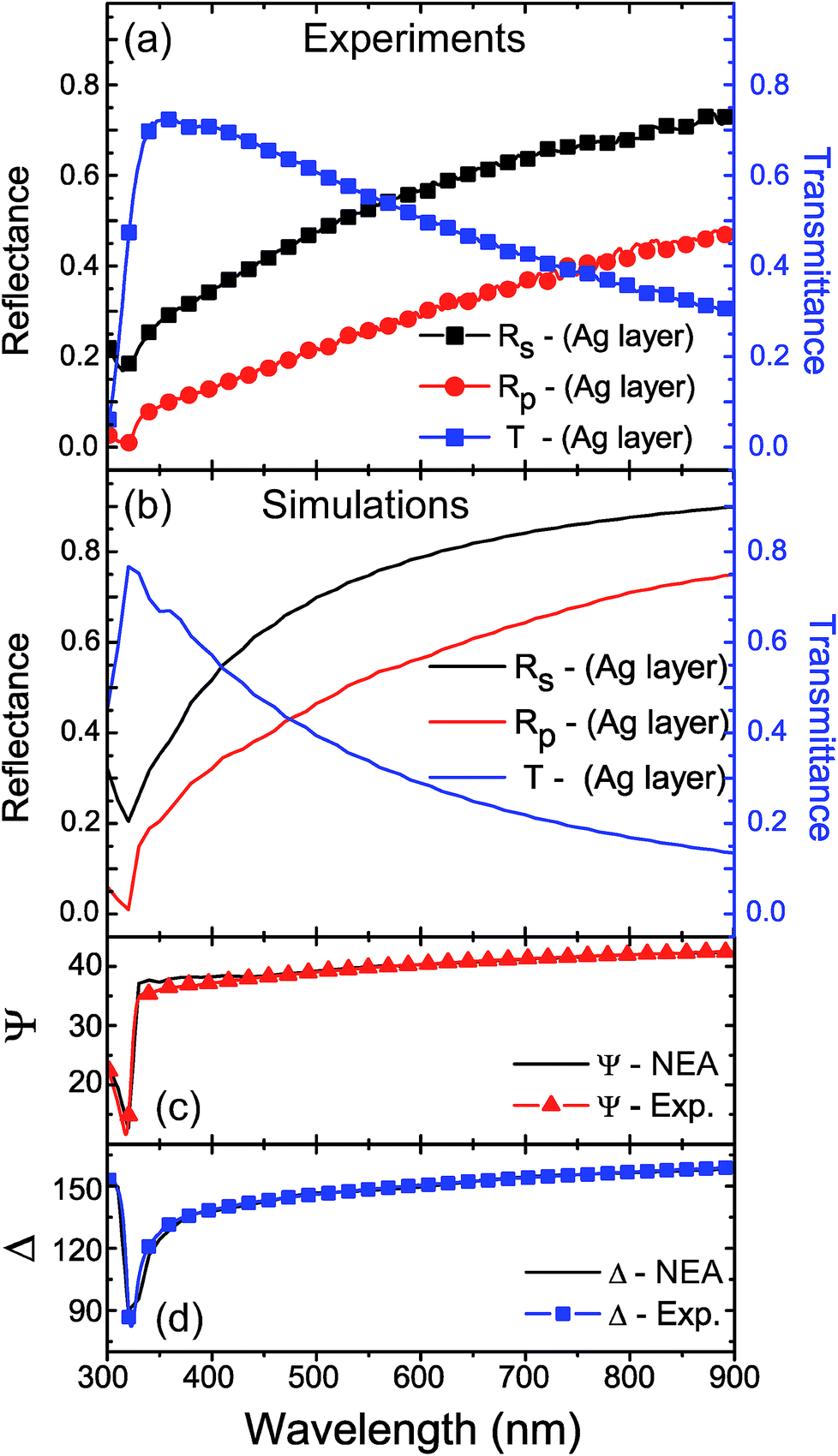 | ||
| Fig. 2 Reflectances (Rp, and Rs, red and black lines with symbols) and transmittance (T, blue lines with squares) measured (a) and calculated using the NEA model (b) for a single Ag layer on a glass substrate. Comparison between Ψ and Δ for the experimental (colored triangles and squares) and numerical (black lines) cases respectively, for the same samples (c and d). | ||
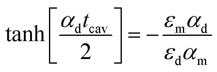
The second test of our NEA model was conducted on a hyperbolic metamaterial (HMM) that, by alternating lossy metal layers with dielectric ones, acquires particular optical features. Thickness and composition of the nanolayers can be opportunely designed in order to exploit unusual optical properties in a desired spectral range. In fact, the particular design and choice of sizes and constitutive materials leads to the epsilon-near-zero-and-pole (εNZP) HMM,41–43 allowing extraordinary light confinement properties. The proposed HMM system is sketched in the inset of Fig. 3b and is composed of five Ag/ITO bilayers, characterized by a fill fraction of 50%. Fig. 3a and b show, respectively, the experimental and numerical reflectances (Rp, and Rs) and the transmittance (T) calculated by the NEA model together with the comparison between experimental and numerical Ψ and Δ for the same sample (Fig. 3c and d). Also in this case, all measured quantities show impressive agreement with their numerical counterparts. Fig. 3e and f show the electric field maps respectively for an s-pol and a p-pol wave at λ = 390 nm, where it is clearly evident that the p-pol wave is able to penetrate more efficiently through the HMM structure than in the s-pol case, where the wave is transmitted by the medium in accordance with the metamaterial prediction.44–47
 | ||
| Fig. 3 Reflectances (Rp, and Rs, red and black lines with symbols) and transmittance (T, blue lines with squares) measured (a) and calculated using the NEA model (b) for the five bilayers Ag/ITO HMM, as sketched in the inset. Comparison between experimental (colored lines with symbols) and numerical systems (solid lines) Ψ (c) and Δ (d), for the same sample. (e and f) Electric field maps distribution for TE (s-pol) and TM (p-pol) waves respectively, extracted for an impinging wavelength of 390 nm. | ||
A further and more complex test of the NEA model has been performed by considering the third system where every kind of thickness periodicity is absent. This choice reflects a more typical experimental situation with different thicknesses of all the layers and materials involved. The sample was composed of a unit cell of three materials, Ag, ITO and AZO, repeated three times, where the thickness of each layer was different (see inset of Fig. 4b). Starting from the glass substrate, the layer thicknesses were: 19 nm (Ag), 15 nm (ITO), 15 nm (AZO), 20 nm (Ag), 21 nm (ITO), 16 nm (AZO), 23 nm (Ag), 27 nm (ITO) and 15 nm (AZO). Fig. 4 reports the results related to this sample; the agreement between experiments and simulations is also quite remarkable in this case. The numerical ellipsometer simulation represents a real chance to overcome the typical theoretical approach based on the Transfer Matrix Method (TMM), that becomes particularly cumbersome when an additional 2D or 3D periodical structure is placed on top of the most external metamaterial surface. With this aim, the user-friendly interface allows positioning, without particular effort, nanostructures of different shapes and sizes on the top surface, and the proposed NEA tool allows the study of how the transmitted signal is affected by them.48–51 In the fourth considered case, we simulated the optical behavior of an asymmetric multi-layer that does not respect the typical metamaterial fill fraction condition. In fact, when one of the layers is much thicker than the other ones, nanometric cavity behavior comes in, enabling confinement and re-direction of light. This kind of metamaterial opens a new challenge in obtaining nanometric devices with particular optical features suitable for applications. In our case, two different systems have been realized, that are able to work at two or three different wavelengths, depending on the thickness of the thick-ITO layer. The first nanocavity (t1 = 230 nm) is able to confine two different working wavelengths, λ = 390 nm and 550 nm, while the second one (t2 = 350 nm) shows a three wavelengths confinement (λ = 410 nm, 520 nm and 750 nm). We indicated these systems as two- and three-bands metamaterials (2BMM and 3BMM, respectively). The two samples were fabricated by starting with a 20 nm Ag layer deposited on a glass substrate. Then, different thick-ITO slabs (t1 and t2) were deposited. Light confinement was achieved by putting a final Ag/thin-ITO (20/20) bilayer, of 40 nm total thickness, on top of the thick-ITO slabs, obtaining the final 2BMM and 3BMM systems, respectively. The two configurations presented unique optical behaviors that were also verified by the numerical model. The experimental analysis was carried out as a function of the incident angles (50°, 60° and 70°), under which the p-pol reflectances were measured (Fig. 5c and d refer to the 2BMM and the 3BMM, respectively). As the incident angle increases, a blue shift of the reflectance dips is observed, due to the gap surface plasmons (gsp) that are able to establish guiding modes in the ITO thick slabs with t1 (2BMM) and t2 (3BMM) thicknesses. In the presence of an optical cavity, confined modes satisfy the general Fabry–Perot (FP) condition βtcav = mπ − ϕ, where β is the complex wave-vector of the lightwave propagating within the cavity, m identifies the given mode generated inside the cavity, ϕ is the reflection dephase angle and tcav is the cavity thickness. In this case, the FP relation, applied to a nanocavity confined by metal layers,52 is modified as in the following, βgsptcav = mπ − ϕ, where βgsp is calculated by considering the dispersion relation of a general MIM structure:
 | (3) |
 , where the subscript m and d refer to the metal and dielectric layers, respectively. The evaluation of βgsp in our cases is reported in the ESI† with the related dispersion graphs (Fig. S2a and c†) and the surface plasmon modes calculations (Fig. S2b and d†).53–61 In Fig. S2b (ESI†), the modal analysis is reported for the 2BMM, from which it is possible to extract the observed modes. The obtained modes confirm the results shown in Fig. 5a: for m ∼ 3, λ = 390 nm, while λ = 550 nm corresponds to the mode m ∼ 2. For the 3BMM (tcav = 350 nm), the results derived from Fig. S2d† are in agreement with those shown in the electric field maps of Fig. 5b: m ∼ 4 is related to λ = 410 nm, m ∼ 3 to λ = 520 nm and m ∼ 2 to λ = 750 nm. These confined modes are depicted as black curves on the electric field distribution maps reported in Fig. 5a and b. A qualitative confirmation of this fact is given by the spectral position of the dips present in the reflectance curves (Fig. 5c and d) that correspond to the working wavelengths mentioned above, for the 2BMM and the 3BMM, respectively. The curves shown in Fig. 5e and f highlight a value of transmitted light overcoming, for the first system, 60% at λ = 550 nm in the cases of both experiment and simulation. The second cavity instead presents a larger difference at λ = 520 nm between the experimental and simulated systems, even if the transmitted signal still reaches a noticeable 50% value in the real case. We underline that, in specific spectral windows, the presented systems show transmittance values proportionally much higher than in a single Ag layer (20 nm). However, it should be noted that, passing through a nanocavity, light runs into two metal layers (20 nm each) and two (thick and thin) ITO slabs, corresponding to hundreds of nanometers (Fig. 2a, blue squares). The surprisingly high signal transmitted by these asymmetric nanocavities thus evidences their optical behavior as originating from an unusual effective medium. The slight amplitude mismatch between the experimental and numerical reflectance dips and transmittance peaks observed in Fig. 5d and f (3BMM) is probably due to a collapse of the ITO slab in the Ag layer, causing an overall reduction of their effective thicknesses. The field maps and reflectance for s-pol, as well as the comparison of Ψ and Δ between the experiments and the numerical simulations, are reported in the ESI (Fig. S3†); the reflectance curves are also characterized by the same number of dips for this “out-of-plane” polarization. The trend of Ψ presents two or three sigmoidal features corresponding to the number and position of dips in reflectance for both polarizations (Rp and Rs). The same behavior is present in the phase-shift reported in the Δ curves (Fig. S3e and f†).
 | ||
| Fig. 4 Reflectances (Rp, and Rs, red and black lines with symbols) and transmittance (T, blue lines with squares) measured (a) and calculated using the NEA model (b) for the metamaterial with a three-material unit cell (AZO/ITO/Ag). In the inset, a 3D sketch of the sample is reported. Comparison between experimental (colored lines with symbols) and numerical systems (solid lines) Ψ (c) and Δ (d), for the same sample. | ||
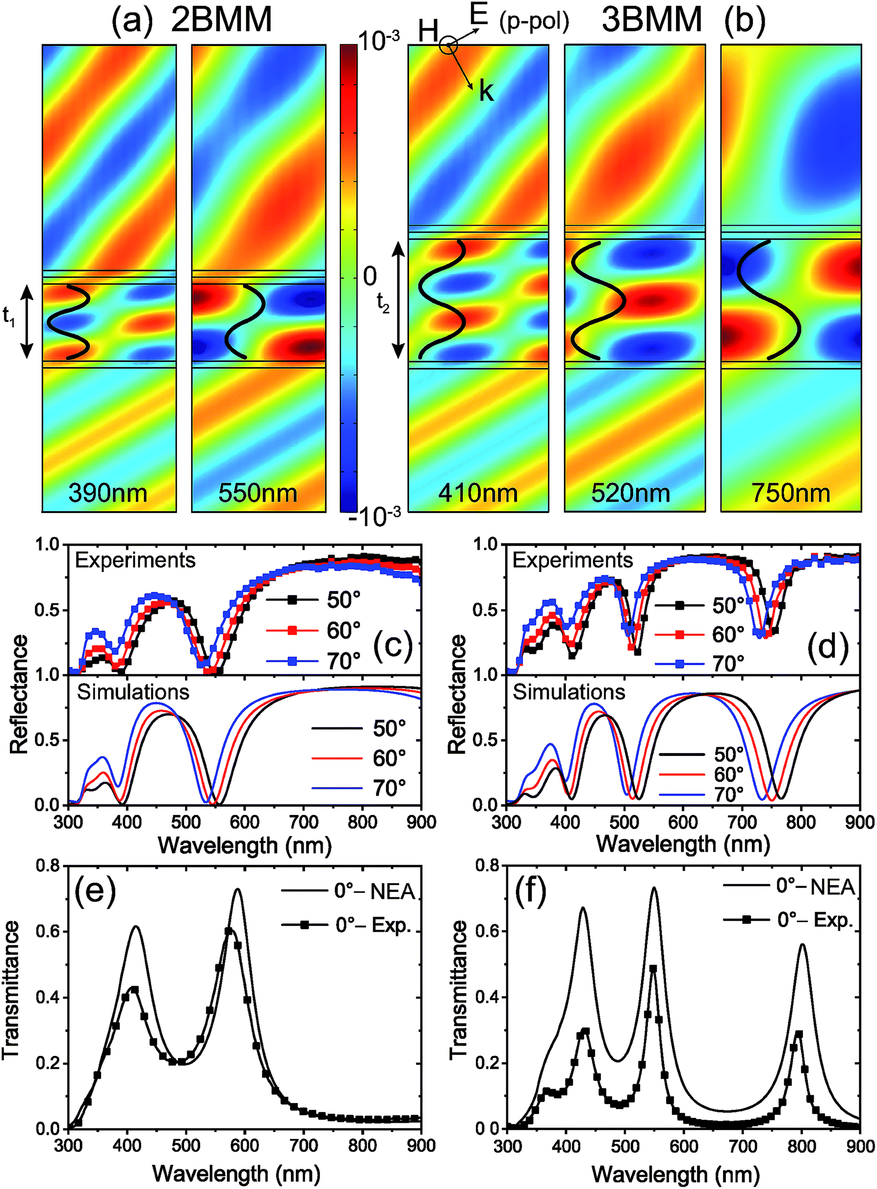 | ||
| Fig. 5 Electric field maps distribution for the 2BMM (a) and 3BMM (b) systems. The black solid lines marked on the field maps represent the even and odd modes supported by the nanometric cavities. Rp reflectances at different angles of incident light, measured and calculated using the NEA model for the 2BMM and the 3BMM, are reported in (c) and (d) respectively. Comparison between experimental and numerical transmittances for the 2BMM and the 3BMM are reported in (e) and (f) respectively. | ||
It is worth noting that the interesting simultaneous presence of dips in the p- and s-pol reflectance curves shown by this MIM structure are independent from the impinging light polarization direction. As such, these results can be exploited to realize sensors or photovoltaic cells that are able to work in a wide UV-VIS-NIR range.48,62–67 In order to complete the numerical analysis of the 3BMM structure, we performed a parametric study of reflectance and transmittance of the system as a function of wavelength (λi) and incidence angle (θi) of the incoming EM wave in the visible range. The resulting reflectance map, shown in Fig. 6a, reveals the coupling between the impinging light and the 3BMM, evidenced by the three permitted wavelength bands for incident angles ranging between 0° and 85°. Position and number of these bands are strongly related to the thickness of the cavity. For instance, if the thickness is reduced to about 200–300 nm, the dip located around λ = 750 nm disappears, as shown by the 2BMM (Fig. 5c); for a thickness of about 400 nm the wavelength of the same dip is instead shifted to around λ = 800 nm. Fig. S4 of the ESI† demonstrates how sensitive the spectral position is of a given reflectance dip of the 3BMM as a function of the cavity thickness. By considering an incident angle of θi = 50° and varying the cavity thickness from 218 nm to 242 nm, it is possible to move the reflectance dip by Δλ = 40 nm, from 535 nm to 575 nm. Fig. S4b† reports the linear trend of the cavity working wavelength as a function of the cavity thickness. By keeping the cavity thickness fixed, the spectral position of the reflectance dips can also be influenced by the presence of a material on top of the 3BMM surface. This suggests the possible utilization of this system as a sensor for refractive index variations. In order to verify this possibility and carry out a further performance check on the developed tool, we numerically designed another 3BMM structure with 10 nm of AZO placed on its top surface. For this test, the more sensitive confined mode (m ∼ 2 at λ = 750 nm) was selected. By impinging at the Brewster angle (60°, white dashed line in Fig. 6a) and with p-polarized light on the structure, the reflectance curve obtained in the presence of the AZO coating (dashed-dot red line in Fig. 6b) shows a clearly evident redshift of about 10 nm with respect to the curve for the system without the coating (black solid line in Fig. 6b). As a final remark, the exploitation of a generic N-BMM structure for applications presents many benefits: (i) the position and amplitude (depth) of the transmittance (reflectance) are directly correlated to the thickness of the ITO slab; (ii) these transmittance peaks (reflectance dips) have been obtained without the presence of 3D structures on the material surface to couple the impinging light in; (iii) the system is independent from the impinging light polarization; (iv) the fabrication process used to realize the structures is fast and cost-effective.
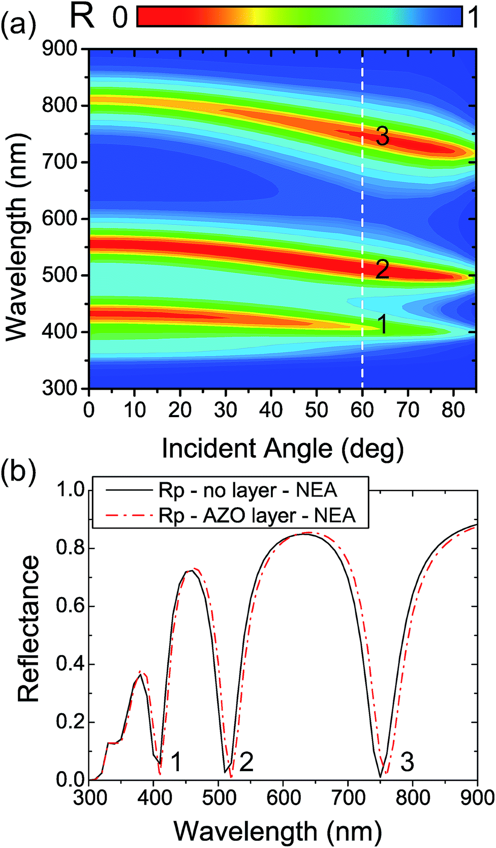 | ||
| Fig. 6 (a) Reflectance map calculated by varying the incident wavelength λi and angle θi. The dashed white line drawn on the field map indicates the position of the Brewster angle for this structure that has been used as the incident angle in the numerical simulations whose results are reported in the graph. (b) Rp reflectances calculated for the sensor realized by using the 3BMM with and without an AZO coating layer of 10 nm on its top surface (solid black and dashed-dot red lines, respectively). | ||
4 Conclusions
In this contribution, we have presented a comprehensive optical analysis of different nanoscale structures. We propose a solid numerical tool, based on the COMSOL Multiphysics platform, that is able to predict the optical behavior of real case studies. As a crucial test-bed of the tool, optical features such as reflectance, and transmittance, as well as the ellipsometric angles Ψ and Δ have been calculated in the presence of systems with increasing structural complexities, from single metal layers to asymmetric multi-layers behaving as optical nanocavities for light. The latter configuration shows a peculiar metamaterial behaviour originating from its unusual effective medium properties, that can be efficiently exploited in sensors applications. Indeed, in specific spectral windows, the asymmetric multi-layer with a full thickness of hundreds of nanometers shows a hyper transmission of light with respect to a single 20 nm-thick Ag layer. The resulting comprehensive analysis of the considered nanoscale systems has shown an excellent agreement between numerical and experimental curves, as detailed by the comparative tables reported in the ESI.† This confirms the effectiveness of the tool as a significant instrument for nanotechnology design and fundamental research in nanoscience.Conflicts of interest
There are no conflicts to declare.Acknowledgements
The authors thank G. Strangi and V. Caligiuri for fruitful discussions. They also thank the Area della Ricerca di Roma 2, Tor Vergata, for the access to the ICT Services (ARToV-CNR) for the use of the COMSOL Multiphysics Platform, Origin Lab and Matlab, and the Infrastructure BeyondNano (PONa3-00362) of CNR-Nanotec for the access to research instruments.References
- W. B. Zimmerman, Process modelling and simulation with finite element methods, World Scientific, 2004, vol. 1 Search PubMed.
- J.-M. Jin, The finite element method in electromagnetics, John Wiley & Sons, 2015 Search PubMed.
- F. D’apuzzo, M. Esposito, M. Cuscunà, A. Cannavale, S. Gambino, G. E. Lio, A. De Luca, G. Gigli and S. Lupi, ACS Photonics, 2018, 2431–2436 CrossRef.
- E. Oñate, Structural analysis with the finite element method: linear statics, 2009, pp. 1–42 Search PubMed.
- J. Donea, S. Giuliani and J.-P. Halleux, Comput. Methods Appl. Mech. Eng., 1982, 33, 689–723 CrossRef.
- C. Taylor and P. Hood, Comput. Fluids, 1973, 1, 73–100 CrossRef.
- J. N. Reddy and D. K. Gartling, The finite element method in heat transfer and fluid dynamics, CRC Press, 2010 Search PubMed.
- V. Mengeaud, J. Josserand and H. H. Girault, Anal. Chem., 2002, 74, 4279–4286 CrossRef CAS.
- H. Park, Study of Surface Plasmon Resonance in Metal and Alloy Nanofilms Using Maxwell Description and Metamaterial Simulation in COMSOL, Rose-Hulman Institute of Technology, 2015 Search PubMed.
- M. Asle-Zaeem and S. D. Mesarovic, Solid State Phenom., 2009, 29–41 CAS.
- A. Ferraro, D. C. Zografopoulos, R. Caputo and R. Beccherelli, Sci. Rep., 2018, 8, 17272 CrossRef.
- G. E. Lio, G. Palermo, R. Caputo and A. De Luca, J. Appl. Phys., 2019, 125, 082533 CrossRef.
- G. E. Lio, J. B. Madrigal, X. Xu, Y. Peng, S. Pierini, C. Couteau, S. Jradi, R. Bachelot, R. Caputo and S. Blaize, J. Phys. Chem. C, 2019, 123, 14669–14676 CrossRef CAS.
- K. M. Hoogeboom-Pot, J. N. Hernandez-Charpak, X. Gu, T. D. Frazer, E. H. Anderson, W. Chao, R. W. Falcone, R. Yang, M. M. Murnane, H. C. Kapteyn and D. Nardi, Proc. Natl. Acad. Sci. U. S. A., 2015, 112, 4846–4851 CrossRef CAS.
- Y. Hu, L. Zeng, A. J. Minnich, M. S. Dresselhaus and G. Chen, Nat. Nanotechnol., 2015, 10, 701 CrossRef CAS.
- G. Palermo, U. Cataldi, A. Condello, R. Caputo, T. Bürgi, C. Umeton and A. De Luca, Nanoscale, 2018, 16556–16561 RSC.
- G. Jellison Jr, Thin Solid Films, 1998, 313, 33–39 CrossRef.
- G. Jellison Jr, V. Merkulov, A. Puretzky, D. Geohegan, G. Eres, D. Lowndes and J. Caughman, Thin Solid Films, 2000, 377, 68–73 CrossRef.
- P. Washington, H. Ong, J. Dai and R. Chang, Appl. Phys. Lett., 1998, 72, 3261–3263 CrossRef CAS.
- G. Jellison Jr and F. Modine, Appl. Phys. Lett., 1996, 69, 371–373 CrossRef.
- R. Collins and B. Yang, J. Vac. Sci. Technol., B: Microelectron. Process. Phenom., 1989, 7, 1155–1164 CrossRef CAS.
- J. De Feijter, d. J. Benjamins and F. Veer, Biopolymers, 1978, 17, 1759–1772 CrossRef CAS.
- D. Aspnes, J. Theeten and F. Hottier, Phys. Rev. B: Condens. Matter Mater. Phys., 1979, 20, 3292 CrossRef CAS.
- M. D. Porter, T. B. Bright, D. L. Allara and C. E. Chidsey, J. Am. Chem. Soc., 1987, 109, 3559–3568 CrossRef CAS.
- G. Jellison Jr, Opt. Mater., 1992, 1, 41–47 CrossRef.
- G. Jellison and L. Boatner, Phys. Rev. B: Condens. Matter Mater. Phys., 1998, 58, 3586 CrossRef CAS.
- D. Aspnes, J. Opt. Soc. Am. A, 1993, 10, 974–983 CrossRef.
- L. De Sio, V. Caligiuri and C. Umeton, J. Opt., 2014, 16, 065703 CrossRef.
- G. Rana, P. Deshmukh, S. Duttagupta and S. Prabhu, Design of a Simple and Robust Asymmetric Ellipsometer for Terahertz (THz) using COMSOL Ray Optics Module, 2015, http://https://www.comsol.it/paper/download/295461/rana_paper.pdf Search PubMed.
- H. Wiklund, H. Arwin and K. Järrendahl, Phys. Status Solidi A, 2008, 205, 945–948 CrossRef CAS.
- H. Gross, R. Model, M. Baer, M. Wurm, B. Bodermann and A. Rathsfeld, Measurement, 2006, 39, 782–794 CrossRef.
- H. Fujiwara, Spectroscopic ellipsometry: principles and applications, John Wiley & Sons, 2007 Search PubMed.
- H. Tompkins and E. A. Irene, Handbook of ellipsometry, William Andrew, 2005 Search PubMed.
- W. B. Zimmerman, Multiphysics modeling with finite element methods, World Scientific Publishing Company, 2006, vol. 18 Search PubMed.
- M. Losurdo and K. Hingerl, Ellipsometry at the nanoscale, Springer, 2013 Search PubMed.
- G. R. Fowles, Introduction to modern optics, Courier Corporation, 1975 Search PubMed.
- V. Caligiuri and A. De Luca, J. Phys. D: Appl. Phys., 2016, 49, 08LT01 CrossRef.
- V. Caligiuri, M. Palei, M. Imran, L. Manna and R. Krahne, ACS Photonics, 2018, 2287–2294 CrossRef CAS.
- Z. Han, E. Forsberg and S. He, IEEE Photonics Technol. Lett., 2007, 19, 91–93 Search PubMed.
- W. D. Newman, C. L. Cortes, J. Atkinson, S. Pramanik, R. G. DeCorby and Z. Jacob, ACS Photonics, 2014, 2, 2–7 CrossRef.
- L. Sun and K. Yu, J. Opt. Soc. Am. B, 2012, 29, 984–989 CrossRef CAS.
- L. Sun, X. Yang and J. Gao, Appl. Phys. Lett., 2013, 103, 201109 CrossRef.
- P. Shekhar, J. Atkinson and Z. Jacob, Nano Convergence, 2014, 1, 14 CrossRef PubMed.
- J. Valentine, S. Zhang, T. Zentgraf, E. Ulin-Avila, D. A. Genov, G. Bartal and X. Zhang, nature, 2008, 455, 376 CrossRef CAS.
- V. M. Shalaev, W. Cai, U. K. Chettiar, H.-K. Yuan, A. K. Sarychev, V. P. Drachev and A. V. Kildishev, Opt. Lett., 2005, 30, 3356–3358 CrossRef PubMed.
- S. Zhang, W. Fan, N. Panoiu, K. Malloy, R. Osgood and S. Brueck, Phys. Rev. Lett., 2005, 95, 137404 CrossRef.
- B. J. Justice, J. J. Mock, L. Guo, A. Degiron, D. Schurig and D. R. Smith, Opt. Express, 2006, 14, 8694–8705 CrossRef.
- K. V. Sreekanth, A. De Luca and G. Strangi, Sci. Rep., 2013, 3, 3291 CrossRef.
- W. Adams, A. Ghoshroy and D. Ö. Güney, ACS Photonics, 2018, 5, 1294–1302 CrossRef CAS.
- L. Shen, H. Wang, R. Li, Z. Xu and H. Chen, Sci. Rep., 2017, 7, 6995 CrossRef.
- V. Caligiuri, L. Pezzi, A. Veltri and A. De Luca, ACS Nano, 2016, 11, 1012–1025 CrossRef.
- V. J. Sorger, R. F. Oulton, J. Yao, G. Bartal and X. Zhang, Nano Lett., 2009, 9, 3489–3493 CrossRef CAS.
- S. I. Bozhevolnyi, Opt. Express, 2006, 14, 9467–9476 CrossRef PubMed.
- Y. Kurokawa and H. T. Miyazaki, Phys. Rev. B: Condens. Matter Mater. Phys., 2007, 75, 035411 CrossRef.
- J.-Q. Liu, L.-L. Wang, M.-D. He, W.-Q. Huang, D. Wang, B. Zou and S. Wen, Opt. Express, 2008, 16, 4888–4894 CrossRef PubMed.
- S. S. Senlik, A. Kocabas and A. Aydinli, Opt. Express, 2009, 17, 15541–15549 CrossRef CAS.
- M. Kuttge, W. Cai, F. J. G. de Abajo and A. Polman, Phys. Rev. B: Condens. Matter Mater. Phys., 2009, 80, 033409 CrossRef.
- S. Vassant, A. Archambault, F. Marquier, F. Pardo, U. Gennser, A. Cavanna, J.-L. Pelouard and J.-J. Greffet, Phys. Rev. Lett., 2012, 109, 237401 CrossRef CAS.
- G. Tagliabue, C. Höller, H. Eghlidi and D. Poulikakos, Nanoscale, 2014, 6, 10274–10280 RSC.
- C. L. Smith, N. Stenger, A. Kristensen, N. A. Mortensen and S. I. Bozhevolnyi, Nanoscale, 2015, 7, 9355–9386 RSC.
- S. Refki, S. Hayashi, A. Rahmouni, D. V. Nesterenko and Z. Sekkat, Plasmonics, 2016, 11, 433–440 CrossRef CAS.
- V. Talwar, O. Singh and R. C. Singh, Sens. Actuators, B, 2014, 191, 276–282 CrossRef CAS.
- M. Hjiri, R. Dhahri, K. Omri, L. El Mir, S. Leonardi, N. Donato and G. Neri, Mater. Sci. Semicond. Process., 2014, 27, 319–325 CrossRef CAS.
- E. J. Klem, J. S. Lewis and D. Temple, Infrared Technology and Applications XXXVI, 2010, p. 76602E Search PubMed.
- C. E. Kim, P. Moon, S. Kim, J.-M. Myoung, H. W. Jang, J. Bang and I. Yun, Thin Solid Films, 2010, 518, 6304–6307 CrossRef CAS.
- K. Sreekanth, A. De Luca and G. Strangi, J. Opt., 2014, 16, 105103 CrossRef.
- K. V. Sreekanth, Y. Alapan, M. ElKabbash, E. Ilker, M. Hinczewski, U. A. Gurkan, A. De Luca and G. Strangi, Nat. Mater., 2016, 15, 621 CrossRef CAS.
Footnote |
| † Electronic supplementary information (ESI) available. See DOI: 10.1039/c9ra03684a |
| This journal is © The Royal Society of Chemistry 2019 |