
 Open Access Article
 This Open Access Article is licensed under a Creative Commons Attribution-Non Commercial 3.0 Unported Licence
Role of polysilicon in poly-Si/SiOx passivating contacts for high-efficiency silicon solar cells
HyunJung Park *a,
Soohyun Baea,
Se Jin Parka,
Ji Yeon Hyuna,
Chang Hyun Leea,
Dongjin Choia,
Dongkyun Kanga,
Hyebin Hana,
Yoonmook Kang†
b,
Hae-Seok Lee†b and
Donghwan Kim†ab
*a,
Soohyun Baea,
Se Jin Parka,
Ji Yeon Hyuna,
Chang Hyun Leea,
Dongjin Choia,
Dongkyun Kanga,
Hyebin Hana,
Yoonmook Kang†
b,
Hae-Seok Lee†b and
Donghwan Kim†ab
aDepartment of Materials Science and Engineering, Korea University, Seoul 02841, Republic of Korea. E-mail: jung1029@korea.ac.kr; Tel: +02 3290 3713
bKU-KIST Green School Graduate School of Energy and Environment, Korea University, Seoul 02841, Republic of Korea
First published on 26th July 2019
Abstract
In this study, we focused on understanding the roles of a polysilicon (poly-Si) layer in poly-Si/SiOx/c-Si passivating contacts. Passivating contact formation conditions were varied by changing the doping method, annealing temperature and time, polysilicon layer thickness, and polysilicon doping concentration. Our observations indicated that the roles of polysilicon are contact, in-diffusion barrier action, field effect, gettering, and light absorption. Based on the observations, a iVOC of 741 mV was obtained. Finally, to increase JSC with high VOC, the polysilicon was etched after hydrogenation to reduce light absorption with high passivation quality. iVOC was not affected by etching; moreover, by etching the polysilicon from 300 nm to 60 nm, the cell efficiency increased from 20.48% to 20.59% with increasing JSC, constant VOC, and fill factor.
1 Introduction
As the theoretical efficiency limit for silicon solar cells is approaching,1 various solar cell structures and fabrication methods are being studied. In a solar cell, carriers are generated by incident light and collected on external electrodes. In this process, electrons and holes are separately collected on each electrode by carrier selectivity.2 For a conventional structure of silicon solar cell with aluminum back surface field (Al-BSF), recombination loss at the metal–semiconductor junction is the major cause of efficiency loss owing to the high interface defect density at the metal/silicon interface.3–5 To reduce the recombination loss, passivating contacts (also referred to as carrier-selective contacts) have been introduced for high-quality passivation with low contact resistance.2,5–14 The passivating contact cells differ from conventional cells in the following ways: (1) the recombination occurring at the metal–semiconductor junction is reduced by a passivation layer between the crystalline silicon and metal contact, and (2) the majority carriers can move to the metal contact, while the minority carriers cannot be moved from crystalline silicon to the metal contact owing to carrier selectivity.The major two passivating contacts use intrinsic amorphous silicon (a-Si) or silicon oxide (SiOx) as a thin passivation layer. Passivating contacts based on a-Si are referred to as heterojunction or HIT.15–18 The SiOx-based passivating contacts consist of SiOx and polycrystalline silicon (poly-Si) in a stack structure, and the cells using poly-Si/SiOx passivating contacts are referred to as tunnel oxide passivated contact (TOPCon),8,19–22 semi-insulating polycrystalline silicon (SIPOS),23,24 polycrystalline silicon on oxide (POLO),25,26 or poly-Si passivating contact.27–30 Additionally, it should be noted that EPFL recently published a study on SiOx-based passivating contact using silicon-rich silicon carbide instead of poly-Si.31 In HIT cells, the highest recorded efficiency for an interdigitated back contact (IBC) structure was 26.7% (ref. 16 and 17) and that for a front and rear contact structure was 24.7%.18 However, heterojunction solar cells have process temperature limits.32–36 Therefore, another passivating contact structure with SiOx/poly-Si, instead of amorphous silicon, has attracted the interest of researchers. In poly-Si passivating contact cells, the highest efficiency of 26.1% and 25.8% for IBC25 and front and rear contact structures17,37 were reported, respectively. This efficiency is remarkable because it is the highest efficiency using the front and rear contact.
With respect to poly-Si passivating contact, many researchers have focused on understanding the characteristics of silicon oxide.9,38–41 In this research, we attempted to focus on poly-Si to understand the relationship between poly-Si and the properties of passivating contact solar cells including electrical and passivation properties. Thus, in this study, we varied the doping method, annealing temperature and time, poly-Si thickness, and doping concentration. For the characterization, we measured the implied open circuit voltage (iVOC), doping concentration profile, and the thickness and crystallinity of poly-Si using quasi-steady-state photoconductance (QSSPC),42 secondary ion mass spectroscopy (SIMS), transmission electron microscopy (TEM), and atom probe tomography (ATP), respectively.
2 Experimental procedure
N-type crystalline silicon wafers grown using the Czochralski method were used. The thickness and resistivity of the wafer were 180 μm and 4.5 Ω cm, respectively. After saw-damage etching using KOH, a silicon oxide layer with a thickness of 1.2 nm was grown on the wafer surface via wet chemical oxidation using H2O2.43 Subsequently, two types of poly-Si layers: intrinsic poly-Si and in situ P-doped poly-Si, were deposited on the silicon oxide surface using low pressure chemical vapor deposition (LPCVD) equipment at 600 °C. The thickness of the intrinsic poly-Si was varied from 50 to 300 nm and POCl3 diffusion was conducted to dope the intrinsic poly-Si. In the pre-deposition step, a POCl3![[thin space (1/6-em)]](https://www.rsc.org/images/entities/char_2009.gif) :O2 gas mixture with varied ratio from 200:800 to 800:200 was used to control the poly-Si doping concentration. The deposition temperature and time were fixed at 740 °C and 20 min, respectively. After pre-deposition, the samples were annealed at temperatures between 800 and 950 °C from 10 to 60 min in a N2 atmosphere. For in situ P-doped poly-Si, the samples were annealed in the same furnace that was used to anneal POCl3-diffused poly-Si in the N2 atmosphere after the deposition of the in situ P-doped poly-Si. The annealing temperature and time were changed from 800 to 950 °C and 10 to 60 min, respectively. After annealing, both POCl3-diffused poly-Si and in situ P-doped poly-Si were dipped in diluted HF acid to etch PSG and native SiOx on poly-Si. Subsequently, the samples were subjected to hydrogenation to further improve the passivation quality by depositing the stacked layers of SiNx and Al2O3 with subsequent annealing at 600 °C for 15 min in a N2 atmosphere. Plasma-enhanced chemical vapor deposition (PECVD) and atomic layer deposition (ALD) were used to deposit SiNx and Al2O3, and rapid thermal process (RTP) was used to anneal them. The stacked layers of SiNx and Al2O3 were removed by dipping in diluted HF. For subsequent experiments on etching poly-Si, an acidic mixture composed of HNO3:H2O:HF = 300:100:10 by volume was used. The passivation quality of the poly-Si contact was analyzed by iVOC, measured using the QSSPC. The doping concentration profile was measured using SIMS measurement. TEM measurement was used to confirm the thickness and crystallinity of the poly-Si. Moreover, after preparing the abovementioned sandwich-structured samples to measure the QSSPC, we fabricated the passivating contact solar cell. The schematics of detailed sample structure and cell structure are presented in Fig. 1.
:O2 gas mixture with varied ratio from 200:800 to 800:200 was used to control the poly-Si doping concentration. The deposition temperature and time were fixed at 740 °C and 20 min, respectively. After pre-deposition, the samples were annealed at temperatures between 800 and 950 °C from 10 to 60 min in a N2 atmosphere. For in situ P-doped poly-Si, the samples were annealed in the same furnace that was used to anneal POCl3-diffused poly-Si in the N2 atmosphere after the deposition of the in situ P-doped poly-Si. The annealing temperature and time were changed from 800 to 950 °C and 10 to 60 min, respectively. After annealing, both POCl3-diffused poly-Si and in situ P-doped poly-Si were dipped in diluted HF acid to etch PSG and native SiOx on poly-Si. Subsequently, the samples were subjected to hydrogenation to further improve the passivation quality by depositing the stacked layers of SiNx and Al2O3 with subsequent annealing at 600 °C for 15 min in a N2 atmosphere. Plasma-enhanced chemical vapor deposition (PECVD) and atomic layer deposition (ALD) were used to deposit SiNx and Al2O3, and rapid thermal process (RTP) was used to anneal them. The stacked layers of SiNx and Al2O3 were removed by dipping in diluted HF. For subsequent experiments on etching poly-Si, an acidic mixture composed of HNO3:H2O:HF = 300:100:10 by volume was used. The passivation quality of the poly-Si contact was analyzed by iVOC, measured using the QSSPC. The doping concentration profile was measured using SIMS measurement. TEM measurement was used to confirm the thickness and crystallinity of the poly-Si. Moreover, after preparing the abovementioned sandwich-structured samples to measure the QSSPC, we fabricated the passivating contact solar cell. The schematics of detailed sample structure and cell structure are presented in Fig. 1.
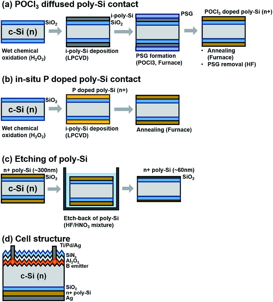 | ||
| Fig. 1 Schematic of sample structure for (a) POCl3-diffused poly-Si contact, (b) in situ P-doped poly-Si contact, (c) etched poly-Si contact, and (d) the final cell structure. | ||
3 Results
3.1 Controlling passivation quality
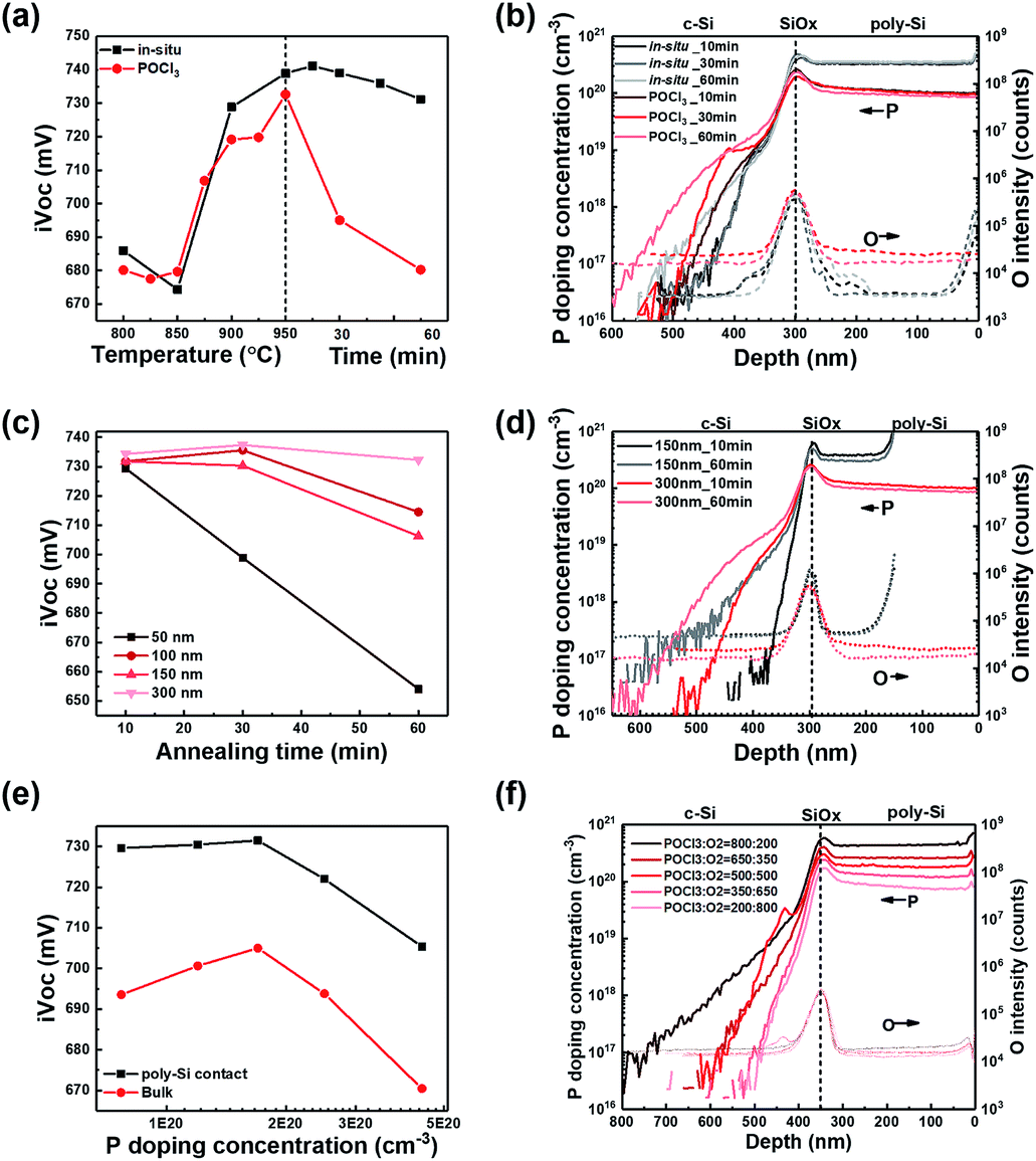 | ||
| Fig. 2 iVOC of poly-Si passivating contacts as a function of (a) annealing temperature, time required for different doping methods, and (c) annealing time for different thicknesses. (e) P doping concentration at poly-Si. (b, d, f) P doping concentration profile (solid line) and oxygen intensity profile (dotted line) of (a, c, e), respectively. | ||
Thus, a different iVOC behavior between in situ P poly-Si and POCl3-diffused poly-Si in the degradation rate of iVOC could be due to the PSG layer. The doping concentration of PSG layer is approximately 1 × 1021 cm−3, which generates three times higher flux because the doping concentration difference between POCl3-diffused poly-Si and in situ P doped poly-Si is three times greater. Owing to this high flux, the dopant atoms diffuse from PSG to poly-Si. This accelerates the deterioration of iVOC as the diffusion of P from poly-Si to c-Si increases, as shown in Fig. 2(d). Consequently, an important role of poly-Si is that of an in-diffusion barrier. It should be noted that the in situ doping method is more suitable owing to a lower extent of in-diffusion.
Additionally, we grew a PSG layer on in situ poly-Si to investigate the effect of a PSG formation step on the characteristics of the poly-Si contact. After growing the PSG layer, it was removed and annealed at 950 °C for 20 min in N2. Consequently, the addition of the PSG growth step decreased the iVOC by 15 mV. This result indicates that the PSG growth step affects passivation quality. A further in-depth study will be required to understand the cause of iVOC due to the addition of the PSG formation step as well as the effect of the PSG growth step on the tunnel oxide or poly-Si layer.
:O2 gas flow rate ratio was changed from 200:800 to 800:200, as shown in Fig. 2(f). The passivation quality increased when the doping concentration was increased from 8 × 1019 cm−3 to 1.8 × 1020 cm−3 but started to decrease rapidly with a further increase in the doping concentration from 1.8 × 1020 cm−3 to 4.5 × 1020 cm−3. This implies that a decrease in iVOC with an increase in doping concentration will be caused by in-diffusion because in-diffusion increases as the doping concentration increases, as shown Fig. 2(f). Additionally, the decrease in iVOC could be due to the precipitates or clusters from the inactive P because the doping concentration at poly-Si is higher than the solubility limit, which is 4 × 1020 cm−3 at 950 °C.44 The reason for the increase in iVOC with an increase in doping concentration is not clearly understood in our study. However, we suggest some possibilities that a high doping concentration would increase the field effect or gettering.
(1) Field effect by doping concentration at poly-Si. According to the TSU-ESAKI tunneling current model,45 the tunneling current is a function of the transmission coefficient (TC), which is determined by calculating the barrier height between c-Si/SiOx and the supply function. These, in turn, are determined using the difference in carrier concentration at the interfaces of the SiOx layer. As the doping concentration at poly-Si changes from 8 × 1019 cm−3 to 2 × 1020 cm−3, the value of ΔEC changes from 0.291 to 0.311 eV. This results in an increase in the electron tunneling current. Therefore, we concluded that the tunneling current changes when the doping concentration at poly-Si changes.
(2) Gettering effect by doping concentration at poly-Si. The gettering effect of the poly-Si passivating contact was studied by A. Liu.10,11 In our research, the gettering effect was confirmed by etching poly-Si/SiOx and the in-diffused region, and re-passivating the sample using a 10 nm-thick aluminum oxide layer. We confirmed that by increasing the doping concentration from 8 × 1019 cm−3 to 1.8 × 1020 cm−3, the bulk quality improved as iVOC after etching the poly-Si/c-Si, from 693 to 705 mV. This implies that a slight increase also caused the gettering effect, with an improvement in the bulk quality. However, further increase in doping concentration caused the drop in bulk iVOC from 710 to 670 mV. This might be caused by the reappearance of gettered impurities, which is also represented by Liu et al.11
Thus, we concluded that poly-Si is required for contact because SiOx would get destroyed without poly-Si. The poly-Si layer plays the following roles: (1) contact, (2) in-diffusion barrier, and provides (3) field effect and (4) gettering. A high-quality passivating contact can be realized using thick poly-Si to reduce in-diffusion and a high doping concentration is used to enhance the passivation quality and gettering effect.
3.2 Effect of hydrogenation
The effect of hydrogenation was investigated by comparing iVOC before and after hydrogenation. In Fig. 3(a–c), delta iVOC represents iVOC after hydrogenation on subtracting iVOC before hydrogenation. Delta iVOC was higher for a lower annealing temperature, shorter time, greater thickness, and lower doping concentration. This implies the following: (1) if the annealing condition is suitable for poly-Si contact with high iVOC, the effect of hydrogenation decreases, and (2) if phosphorus in-diffusion critically affects iVOC, the effect of hydrogenation decreases. Thus, we conclude that in-diffusion is a critical factor that must be avoided for high passivation quality. Moreover, if in-diffusion does not have a critical effect, the annealing condition should be controlled to maximize the passivation quality.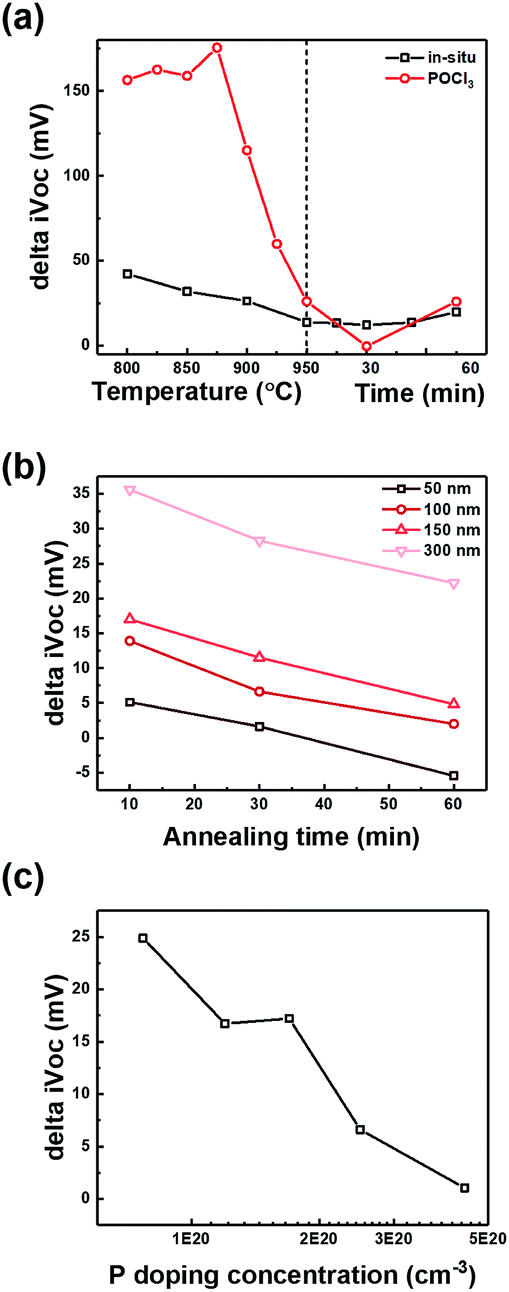 | ||
| Fig. 3 Delta iVOC of poly-Si passivating contacts after and before hydrogenation as a function of (a) annealing temperature, time for different doping methods, and (b) annealing time for different thicknesses, and (c) P doping concentration at poly-Si. | ||
In Fig. 4, 2D and 3D hydrogen concentration profiles of hydrogen atoms were measured using SIMS and ATP, respectively. Fig. 4(a) demonstrates an increase in the concentration of hydrogen atoms at the SiOx layer after hydrogenation. For the 3D profile analysis shown in Fig. 4(b–d), the peak of hydrogen concentration corresponds to that of oxygen concentration. Additionally, a slightly higher hydrogen concentration was confirmed at the surface of poly-Si/SiOx in the 3D mapping as compared to the surface of SiOx/c-Si. In conclusion, the result shows that the position of hydrogen atoms is correlated to the position of oxide layer.
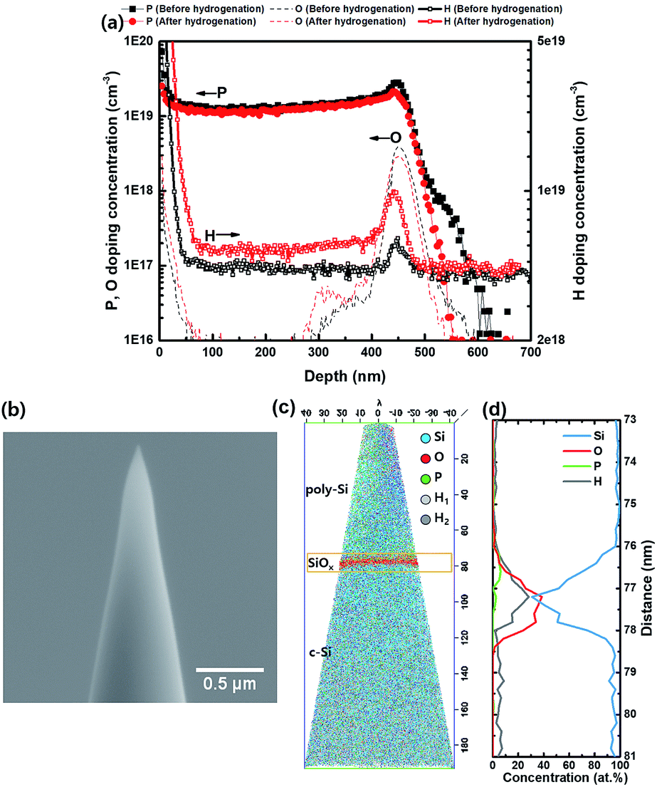 | ||
| Fig. 4 (a) Doping concentration profiles of phosphorus, oxygen, and hydrogen as a function of the depth of the poly-Si passivating contact. Profiles are compared before and after hydrogenation. (b) TEM image of the poly-Si passivating contact and atom probe tomography (APT) measurement result, which shows (c) three-dimensional map of the atoms, (d) one-dimensional doping concentration graph of the interface. | ||
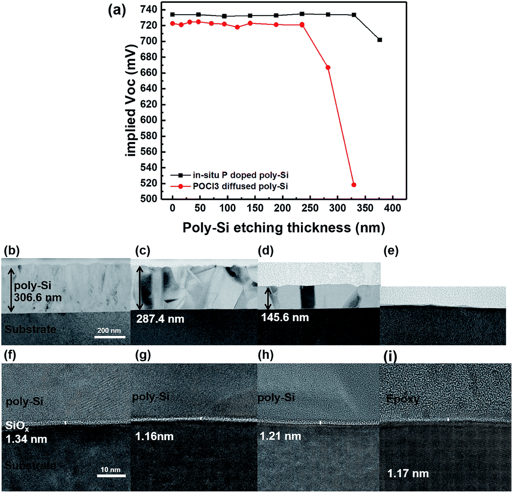 | ||
| Fig. 5 (a) iVOC as a function of poly-Si etching thickness and TEM images of POCl3 diffused poly-Si contacts (b) before annealing, (c) after annealing at 950 °C for 30 min, and after the etching of poly-Si measuring (d) 150 nm and (e) 300 nm. (f, g, h, i) more magnified images of (b, c, d, e), respectively. | ||
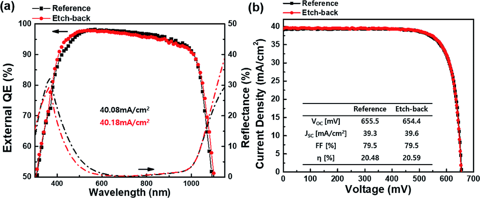 | ||
| Fig. 6 (a) EQE and reflectance graph, and (b) IV curve. | ||
4 Summary
In this study, the roles of poly-Si were elucidated by varying the annealing temperature and time, as well as the thickness and doping concentration of poly-Si. The results indicated that poly-Si played the role of (1) contact, as the different doping concentrations of poly-Si can change the work function and cause different selectivity, (2) barrier layer for metallization and in-diffusion, as poly-Si is needed between SiOx and metal to avoid the destruction of SiOx layer and maintain the passivation quality, and (3) gettering, which improves the bulk quality. Moreover, by analyzing the hydrogenation concentration after hydrogenation, we confirmed that hydrogen passivation at SiOx is important to achieve high iVOC. To further improve the cell efficiency, we etched a poly-Si layer and found that the measured iVOC was not affected after the etching of this layer. By compiling all results, we concluded that the efficiency of the passivating contact silicon solar cell was improved by etching poly-Si via facilitation of high-quality passivation and low IR carrier absorption. Finally, the solar cell exhibited increased efficiency from 20.48% to 20.59% owing to the increased JSC from 39.3 to 39.6 mA cm−2 with a constant VOC and fill factor.Conflicts of interest
There are no conflicts to declare.Acknowledgements
This research was supported by the New & Renewable Energy Core Technology Program of the Korea Institute of Energy Technology Evaluation and Planning (KETEP), a financial grant from the Ministry of Trade, Industry & Energy, Republic of Korea (No. 20163030014020), and the Technology Development Program to Solve Climate Changes of the National Research Foundation (NRF) funded by the Ministry of Science and ICT (NRF-2017M1A2A2087351). This work was supported by the “Human Resources Program in Energy Technology” of the Korea Institute of Energy Technology Evaluation and Planning (KETEP), with financial support from the Ministry of Trade, Industry and Energy, Republic of Korea (No. 20154030200760).References
- A. Richter, M. Hermle and S. W. Glunz, IEEE J. Photovolt., 2013, 3, 1184–1191 Search PubMed.
- U. Würfel, A. Cuevas and P. Würfel, IEEE J. Photovolt., 2014, 5, 1–9 Search PubMed.
- S. W. Glunz and F. Feldmann, Sol. Energy Mater. Sol. Cells, 2018, 185, 260–269 CrossRef CAS.
- X. You-Peng, G. Chao, W. Tao and Z. Lang, Acta Phys. Sin., 2017, 66, 158801 Search PubMed.
- C. Battaglia, A. Cuevas and S. De Wolf, Energy Environ. Sci., 2016, 9, 1552–1576 RSC.
- J. Melskens, B. W. H. van de Loo, B. Macco, L. E. Black, S. Smit and W. M. M. Kessels, IEEE J. Photovolt., 2018, 8, 373–388 Search PubMed.
- F. Feldmann, G. Nogay, J. Polzin, B. Steinhauser, A. Richter, A. Fell, C. Schmiga, M. Hermle and S. W. Glunz, IEEE J. Photovolt., 2018, 8, 1503–1509 Search PubMed.
- F. Feldmann, M. Bivour, C. Reichel, M. Hermle and S. W. Glunz, 28th European PV solar energy conference and exhibition, 2013 Search PubMed.
- U. Römer, R. Peibst, T. Ohrdes, B. Lim, J. Krügener, E. Bugiel, T. Wietler and R. Brendel, Sol. Energy Mater. Sol. Cells, 2014, 131, 85–91 CrossRef.
- A. Liu, D. Yan, S. P. Phang, A. Cuevas and D. Macdonald, Sol. Energy Mater. Sol. Cells, 2018, 179, 136–141 CrossRef CAS.
- A. Liu, D. Yan, J. Wong-Leung, L. Li, S. P. Phang, A. Cuevas and D. Macdonald, ACS Appl. Energy Mater., 2018, 1, 2275–2282 CrossRef CAS.
- D. Yan, A. Cuevas, J. Bullock, Y. Wan and C. Samundsett, Sol. Energy Mater. Sol. Cells, 2015, 142, 75–82 CrossRef CAS.
- B. Nemeth, D. L. Young, M. R. Page, V. LaSalvia, S. Johnston, R. Reedy and P. Stradins, J. Mater. Res., 2016, 31, 671–681 CrossRef CAS.
- F. Feldmann, M. Bivour, C. Reichel, H. Steinkemper, M. Hermle and S. W. Glunz, Sol. Energy Mater. Sol. Cells, 2014, 131, 46–50 CrossRef CAS.
- K. Masuko, M. Shigematsu, T. Hashiguchi, D. Fujishima, M. Kai, N. Yoshimura, T. Yamaguchi, Y. Ichihashi, T. Mishima and N. Matsubara, et al., IEEE J. Photovolt., 2014, 4, 1433–1435 Search PubMed.
- K. Yoshikawa, H. Kawasaki, W. Yoshida, T. Irie, K. Konishi, K. Nakano, T. Uto, D. Adachi, M. Kanematsu, H. Uzu and K. Yamamoto, Nat. Energy, 2017, 2, 17032 CrossRef CAS.
- M. A. Green, Y. Hishikawa, E. D. Dunlop, D. H. Levi, J. Hohl-Ebinger, M. Yoshita and A. W. Ho-Baillie, Prog. Photovoltaics Res. Appl., 2019, 27, 3–12 CrossRef.
- M. Taguchi, A. Yano, S. Tohoda, K. Matsuyama, Y. Nakamura, T. Nishiwaki, K. Fujita and E. Maruyama, IEEE J. Photovolt., 2014, 4, 96–99 Search PubMed.
- K. Masuko, M. Shigematsu, T. Hashiguchi, D. Fujishima, M. Kai, N. Yoshimura, T. Yamaguchi, Y. Ichihashi, T. Mishima and N. Matsubara, et al., IEEE J. Photovolt., 2014, 4, 1433–1435 Search PubMed.
- A. Richter, J. Benick, F. Feldmann, A. Fell, M. Hermle and S. W. Glunz, Sol. Energy Mater. Sol. Cells, 2017, 173, 96–105 CrossRef CAS.
- E. Yablonovitch, T. Gmitter, R. Swanson and Y. Kwark, Appl. Phys. Lett., 1985, 47, 1211–1213 CrossRef CAS.
- A. Rohatgi, B. Rounsaville, Y.-W. Ok, A. M. Tam, F. Zimbardi, A. D. Upadhyaya, Y. Tao, K. Madani, A. Richter and J. Benick, et al., IEEE J. Photovolt., 2017, 7, 1236–1243 Search PubMed.
- P. Brüesch, T. Stockmeier, F. Stucki and P. Buffat, J. Appl. Phys., 1993, 73, 7677–7689 CrossRef.
- L. Elstner, E. Conrad, H. Eschrich, W. Füssel and H. Flietner, Phys. Status Solidi B, 1996, 194, 79–90 CrossRef CAS.
- F. Haase, C. Hollemann, S. Schäfer, A. Merkle, M. Rienäcker, J. Krügener, R. Brendel and R. Peibst, Sol. Energy Mater. Sol. Cells, 2018, 186, 184–193 CrossRef CAS.
- T. Wietler, D. Tetzlaff, J. Krügener, M. Rienäcker, F. Haase, Y. Larionova, R. Brendel and R. Peibst, Appl. Phys. Lett., 2017, 110, 253902 CrossRef.
- G. Yang, A. Ingenito, O. Isabella and M. Zeman, Sol. Energy Mater. Sol. Cells, 2016, 158, 84–90 CrossRef CAS.
- G. Yang, A. Ingenito, N. van Hameren, O. Isabella and M. Zeman, Appl. Phys. Lett., 2016, 108, 033903 CrossRef.
- M. K. Stodolny, J. Anker, B. L. Geerligs, G. J. Janssen, B. W. van de Loo, J. Melskens, R. Santbergen, O. Isabella, J. Schmitz and M. Lenes, et al., Energy Procedia, 2017, 124, 635–642 CrossRef CAS.
- H. Park, H. Park, S. J. Park, S. Bae, H. Kim, J. W. Yang, J. Y. Hyun, C. H. Lee, S. H. Shin and Y. Kang, et al., Sol. Energy Mater. Sol. Cells, 2019, 189, 21–26 CrossRef CAS.
- G. Nogay, J. Stuckelberger, P. Wyss, Q. Jeangros, C. Allebé, X. Niquille, F. Debrot, M. Despeisse, F.-J. Haug, P. Löper and C. Ballif, ACS Appl. Mater. Interfaces, 2016, 8, 35660–35667 CrossRef CAS PubMed.
- A. Ulyashin, R. Job, M. Scherff, M. Gao, W. Fahrner, D. Lyebyedyev, N. Roos and H.-C. Scheer, Thin Solid Films, 2002, 403–404, 359–362 CrossRef CAS.
- K. v. Maydell, E. Conrad and M. Schmidt, Prog. Photovoltaics Res. Appl., 2006, 14, 289–295 CrossRef CAS.
- T. Wang, E. Iwaniczko, M. Page, D. Levi, Y. Yan, H. Branz and Q. Wang, Thin Solid Films, 2006, 501, 284–287 CrossRef CAS.
- M. Jeon, S. Yoshiba and K. Kamisako, Curr. Appl Phys., 2010, 10, S237–S240 CrossRef.
- Y. Lee, S. Han, S. Kim, S. Md Iftiquar, Y.-J. Lee, J. Yoo, A. Dao and J. Yi, J. Photonics Energy, 2014, 4, 043094 CrossRef.
- A. Richter, J. Benick, F. Feldmann, A. Fell, M. Hermle and S. W. Glunz, Sol. Energy Mater. Sol. Cells, 2017, 173, 96–105 CrossRef CAS.
- S. Choi, K. Hong Min, M. Sang Jeong, J. In Lee, M. G. Kang, H.-E. Song, Y. Kang, H.-S. Lee, D. Kim and K.-H. Kim, Sci. Rep., 2017, 7, 12853 CrossRef PubMed.
- H. T. Nguyen, A. Liu, D. Yan, H. Guthrey, T. N. Truong, M. Tebyetekerwa, Z. Li, Z. Li, M. M. Al-Jassim, A. Cuevas and D. Macdonald, ACS Appl. Energy Mater., 2018, 1, 6619–6625 CrossRef.
- A. Moldovan, F. Feldmann, M. Zimmer, J. Rentsch, J. Benick and M. Hermle, Sol. Energy Mater. Sol. Cells, 2015, 142, 123–127 CrossRef CAS.
- H. Steinkemper, F. Feldmann, M. Bivour and M. Hermle, IEEE J. Photovolt., 2015, 5, 1348–1356 Search PubMed.
- R. A. Sinton and A. Cuevas, Appl. Phys. Lett., 1996, 69, 2510–2512 CrossRef CAS.
- H. Kim, S. Bae, K.-s. Ji, S. M. Kim, J. W. Yang, C. H. Lee, K. D. Lee, S. Kim, Y. Kang and H.-S. Lee, et al., Appl. Surf. Sci., 2017, 409, 140–148 CrossRef CAS.
- H. Wagner, A. Dastgheib-Shirazi, B. Min, A. E. Morishige, M. Steyer, G. Hahn, C. del Cañizo, T. Buonassisi and P. P. Altermatt, J. Appl. Phys., 2016, 119, 185704 CrossRef.
- R. Tsu and L. Esaki, Appl. Phys. Lett., 1973, 22, 562–564 CrossRef CAS.
Footnote |
| † These authors contributed equally to this work. |
| This journal is © The Royal Society of Chemistry 2019 |