
 Open Access Article
 This Open Access Article is licensed under a Creative Commons Attribution-Non Commercial 3.0 Unported Licence
Double-layer metal mesh etched by femtosecond laser for high-performance electromagnetic interference shielding window†
Yaqiang Zhangab,
Hongxing Dong*a,
Qisong Lia,
Nanli Mouab,
Lulu Chenab and
Long Zhang *ac
*ac
aKey Laboratory of Materials for High-Power Laser, Shanghai Institute of Optics and Fine Mechanics, Chinese Academy of Sciences, Shanghai, 201800, China. E-mail: hongxingd@siom.ac.cn; lzhang@siom.ac.cn; Fax: +86 21 6957 0216; Tel: +86 21 6906 4137
bCenter of Materials Science and Optoelectronics Engineering, University of Chinese Academy of Sciences, Beijing 100049, China
cIFSA Collaborative Innovation Center, Shanghai Jiao Tong University, Shanghai, China
First published on 17th July 2019
Abstract
An excellent transparent electromagnetic interference (EMI) shielding window is proposed and demonstrated theoretically and experimentally. The window is composed of double layers of Au–Ni composite mesh, separated by the quartz-glass substrate. The simulation exhibits that the shielding effectiveness (SE) of the double-layer mesh can be improved by increasing the thickness of the substrate in the low frequency range far below the first interfere valley. The measured SE of the proposed structure reaches over 37.61 dB covering an ultra-wide frequency ranging from 150 MHz to 5 GHz, with a maximal SE of 75.84 dB at 3.58 GHz, while the average optical transmittance of the double-layer mesh maintains ∼76.35% at 400–900 nm. Moreover, femtosecond laser direct writing processing technology is used to manufacture the double-layer metal grids, the fabricated grids are not easy to be scuffed off and has a longer operating life. Such a high-performance EMI shielding window has great potential applications in precision optical monitoring instrument and military devices.
Introduction
Nowadays, electromagnetic interference (EMI) at radio frequencies has caused a non-negligible negative impact on the lifetimes of civil, commercial and electronic devices as well as human health.1 To reduce such an undesirable impact, EMI shielding technology is used to isolate the human settlements or sophisticated instrument from the EMI sources.2,3 In practical applications, to satisfy the shielding requirement in optical windows and electronic displays for aeronautic, medical, civilian, and research facilities, shielding materials need good optical transmittance while maintaining EMI shielding performance. The development of transparent EMI shielding materials is imperative, but the existing great challenge is how to balance the inherent contradiction between the high optical transmittance and the strong shielding efficiency.4–8 Tremendous efforts have been committed to achieving transparent EMI shielding using a number of strategies and a variety of materials, including transparent conductive oxide, ultra-thin metal films, various shapes of metal grids with micro periods, band-pass frequency selective surface, silver nanowire, graphene and other carbon-based materials.9–14 Among them, indium tin oxide (ITO) is currently used in transparent coating, exhibiting excellent visible light transmittance and strong electromagnetic shielding efficiency. However, ITO has high production cost, poor ultraviolet and infrared transmission that limit its development in window.15,16 Similarly, the inherent conflict between the optical transmittance and shielding efficiency of traditional monolayer metal mesh further restricts its applications.17 Therefore, it still remains a significant technological challenge to achieve high-performance transparent EMI shielding window. Ref. 18 and 19 prove that double-layer metal mesh can enhance EMI shielding performance effectively.18,19Currently, the manufacture methods of the metal mesh for EMI shielding window generally adopt ultraviolet mask lithography or electron beam direct writing methods.20,21 Such methods make the fabricated mesh only deposited on the surface of the substrate, which will lead to low firmness and durability to shorten the operating life. Especially in the face of harsh application environment, such as erosion of wind, rain, sand and stone, will make the shielding layer easy to be scuffed off, resulting in the decrease of shielding performance. To solve this problem, new micromachining methods need to be explored. Femtosecond laser micromachining is a process in which femtosecond laser pulses are focused on the surface or interior of the material to induce micron sized structures. Due to the ultrashort pulse width of femtosecond laser, energy deposition at a time scale is shorter than electron–phonon coupling processes in any materials, which can suppress the formation of heat-affected zone allowing laser processing with high precision and resolution.22–24 The unique advantage of femtosecond laser processing over conventional lithography methods, resides in the capability of focusing under surface or inner of transparent substrates to sculpture deeply complex shapes with grooved structure, both inorganic and organic.25–28 As a consequence, employing femtosecond laser technologies to sculpture metal grids with micro sizes in transparent materials, has a great potential on applications of excellent EMI shielding window.
In this paper, we propose an efficient transparent EMI shielding window based on the double-layer Au–Ni composite mesh. It simultaneously achieves high optical transmittance and strong EMI shielding performance covering an ultra-wide microwave region. The measured SE reaches over 37.61 dB in the whole test frequency band, while the average visible transmittance is ∼76.35%. Moreover, we apply femtosecond laser direct writing processing to fabricate the double-layer mesh. Both the theoretical and experimental results show that the composite mesh has a good application prospect in the field of high-performance transparent EMI shielding materials, which is urgently desirable for modern optoelectronic devices.
Theoretical calculation and simulation
Schematic illustration of the double-layer metal mesh is shown in Fig. 1. Most of microwave and radio waves are reflected by the optical window and almost never pass through it, while visible or infrared light can transmit without being affected. Two layers of square grids are separated by the quartz glass with thickness of h as the dielectric substrate. In order to maintain the balance between the high transparency and excellent EMI shielding performance, the period (p) of metal mesh is only a few hundred micrometres, and the width of the metal line, i.e., d, is several micrometres. Using Au (conductivity σ = 4.1 × 10⁷ S m−1, relative permeability μr = 1) and Ni (conductivity σ = 1.45 × 10⁷ S m−1, relative permeability μr = 600) as the materials of the metal mesh, and the Ni layer is plated below the Au layer. We perform the numerical simulations by Ansoft high frequency structure simulator (HFSS 15.0) software, and the SE of the window is calculated by S-parameter extraction method. S11 and S21 represent the parameters of reflected and transmitted waves, respectively, where reflectivity R = |S11|2 and transmittance T = |S21|2, the equation related to EMI shielding can be written as follows:29
SE (dB) = −10![[thin space (1/6-em)]](https://www.rsc.org/images/entities/char_2009.gif) log10|T| log10|T|
| (1) |
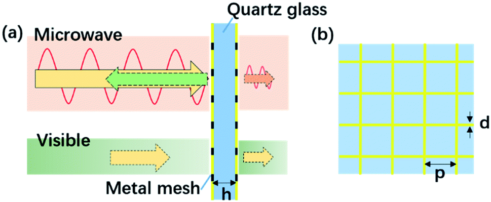 | ||
| Fig. 1 Schematic diagram (a) of the optical window, and detailed structure (b) of the square metal mesh. | ||
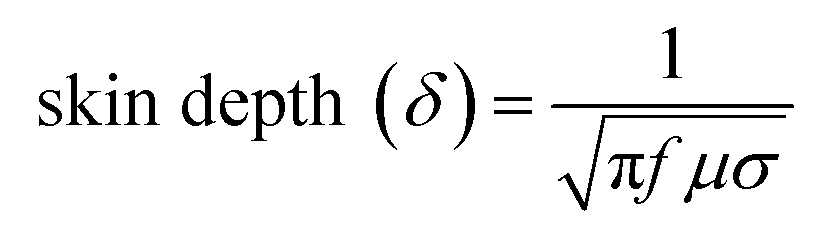
A basic parameter determining shielding performance is the thickness of the metal shielding material which is related to the skin depth. When the thickness of the shielding material is less than the skin depth, the shielding performance will decrease. And the skin depth is the distance the wave travels when the amplitude of the incident electromagnetic wave attenuates to 1/e (approximately 36.8%) of the surface value, which is defined the following equation:29
 | (2) |
We analyse the shielding performance of the double-layer mesh at various quartz glass thickness of h, as shown in Fig. 2(a). Here, the period of the metal mesh is set to p = 200 μm, the line width is d = 10 μm, the thickness of Ni layer is 100 nm, and the thickness of Au layer is 500 nm. It can be seen that the SE of double-layer mesh rapidly increases with the increase of the h from 2 mm to 6 mm at frequency below 10 GHz. When h is further increased, the increasing trends of the SE curves become gradual and even generate resonant peaks at high frequency. Moreover, the first SE resonant peak of the double-layer mesh occurs a shift to low frequency by increasing h, because of the multi-beam interference effect (Fabry–Perot effect). When the electromagnetic wave incidents the double-layer metal mesh, it will penetrate into the upper grids and occurs multiple reflection between two mesh layers to enhance the reflection and dissipation of the incidence. At this point, we use multi-beam interference theory to treat the double-layer metal mesh as a whole film system including the quartz glass substrate. Since the absorption loss is not considered in this theory, the sum of the absorptivity and reflectivity is treated as the equivalent reflectivity of the film system. Under the condition of normal incidence of electromagnetic wave, the equivalent reflectivity of the incident electromagnetic wave is related to optical path difference, that is, the product of the refractive index (n) and the thickness of the equivalent film. The refractive index of the quartz glass is 1.95. The thickness of metal mesh is relatively small, so we use the thickness (h) of quartz glass to describe the thickness of the equivalent film. The relationship between the equivalent reflectivity and the optical thickness of the double-layer mesh, under the normalized incidence with different wavelength (λ), is illustrated in Fig. 2(b). For a specific λ, as shown in the inset of Fig. 2(b), the equivalent reflectivity increases gradually as the equivalent optical thickness of the substrate increases from zero to λ/4, while decreases and generates a resonant peak as the optical thickness is approximately λ/2. When reflectivity increases, the microwave shielding performance will obviously improve. Therefore, the shielding effect of double-layer metal mesh can be maximized by selecting transparent dielectric substrates with appropriate thickness in specific EMI shielding frequency bands.
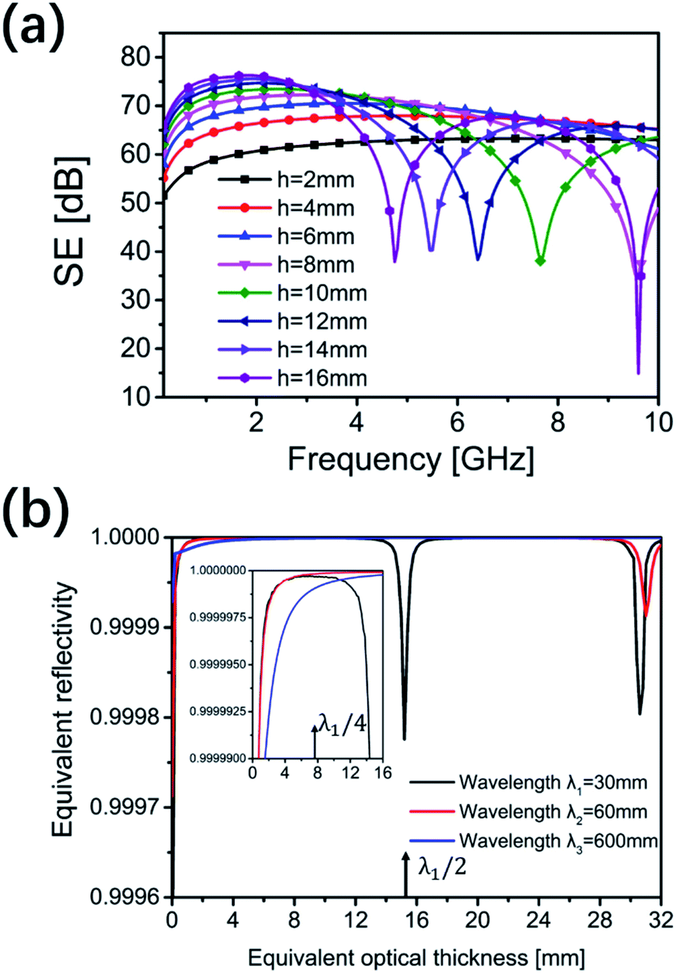 | ||
| Fig. 2 (a) The simulated shielding effectiveness (SE) of the double-layer mesh with various thickness of quartz glass substrate. (b) The simulated reflectivity of the double-layer mesh under normalized incidence with different wavelengths. The period of mesh is 200 μm, the linewidth is 10 μm. The normalized incident wavelengths, λ, are 30 mm (10 GHz frequency), 60 mm (5 GHz frequency), and 600 mm (500 MHz frequency), respectively. | ||
Experiment verification and results
The fabrication processing of the metal mesh on the quartz glass substrate is shown in Fig. 3. Quartz glass circular plate (diameter of 105 mm, thickness of 6 mm) was placed in ethanol and acetone mixture for ultrasonic cleaning for 5 minutes, and the surface was blow-dried with high purity nitrogen. Next, a layer of positive photoresist (RDP-8003, Suzhou Research Material Micro-nano Technology Co. Ltd. China) with thickness of 5 μm was sprayed on the quartz glass film with a spray machine (SC-500-V, Suzhou Meitu Semiconductor Technology Co. Ltd. China), then the substrate was heated baking within 2 minutes to remove the solvent of photoresist, which can also improve the adhesion of the glue.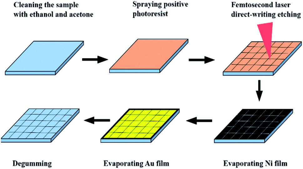 | ||
| Fig. 3 Manufactural process for the metal mesh of the window fabrication. | ||
Microscale square grids were etched by using femtosecond laser direct-writing processing. The schematic diagram of the optical path of the processing system, as shown in Fig. 4. Femtosecond laser direct writing processing system mainly consists of 350 fs femtosecond laser (Spirit High Q Laser, Spectra-Physics Ltd. America), control system, optical path and 3D displacement platform. The sample coated photoresist is placed on a 3D moving control platform and controlled by computer precisely. Before micromachining, the processing surface needed to be modulated horizontally so that the processing plane was on the same horizontal plane. Due to the large thickness of coated film, it was necessary to use femtosecond beam to focus under the surface of quartz glass and etch deeply grids with grooved structure, so as to enhance the adhesion of metal film and prevent it from being scuffed off. Subsequently, the processing period of the grid was set as 200 μm on the software, the repetition times were 2, and the processing speed was 10 mm s−1. During processing, the laser power was 1613 mW, and the repetition frequency was 100 kHz. After that, the machining system runs automatically to finish etching the grid structure.
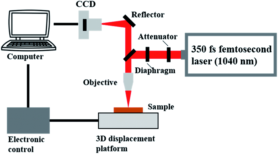 | ||
| Fig. 4 The optical schematic diagram of the femtosecond laser direct writing processing system. | ||
Then, a 100 nm thick Ni layer was evaporated on the surface of quartz glass by electron beam evaporation method, and a 500 nm Au layer was evaporated on the top of the Ni layer. Finally, the sample was placed in N-methyl pyrrolidone (NMP) solution with ultrasonic heating at 65 °C for about 2 minutes to remove residual photoresist, and obtained a complete metal mesh. Similarly, the same machining process is used to fabricate the metal grids on the other surface of the quartz glass.
The fabricated sample is shown in Fig. 5(a), and the “SIOM” logo is clearly visible. Fig. 5(b) demonstrates that the period of the metal grids is 200 μm, measured by 20× objective lens. By measuring with a high magnification precision 100× objective lens, the average line width of the metal wire is approximately 10.5 μm, as shown in Fig. 5(c). In the SEM images of the mesh etched by femtosecond laser on the photoresist and the quartz glass as show in Fig. 5(d) and (e), the width of the grooved structure on the photoresist is approximately 13.4 μm, while that of structure on the quartz glass is about 8.5 μm. The femtosecond laser direct writing micromachining on the photoresist belongs to ablative processing. Since the melting point of photoresist is much smaller than that of quartz glass, the thermal diffusion area of photoresist during ablation is slightly larger than that of quartz glass. In other words, the line width of the grooved structure etched on the photoresist is wider than that etched on the quartz glass. Besides, the edge of the metal mesh during the process of degumming in the ultrasonic process has a little drop of the metal. As a result, the line width of the fabricated metal mesh is slightly smaller than that of the grooved structure on the photoresist. Moreover, in the coating film process, the metal will deposit in the grooved structure, forming a “deep surface-embedded” metal grids. Compared with the metal mesh fabricated by conventional lithographic, the metal mesh sculptured by femtosecond laser has a better attachment on the substrate (Fig. S1 ESI†), which maintains that it has excellent firmness, wear resistance and durability.
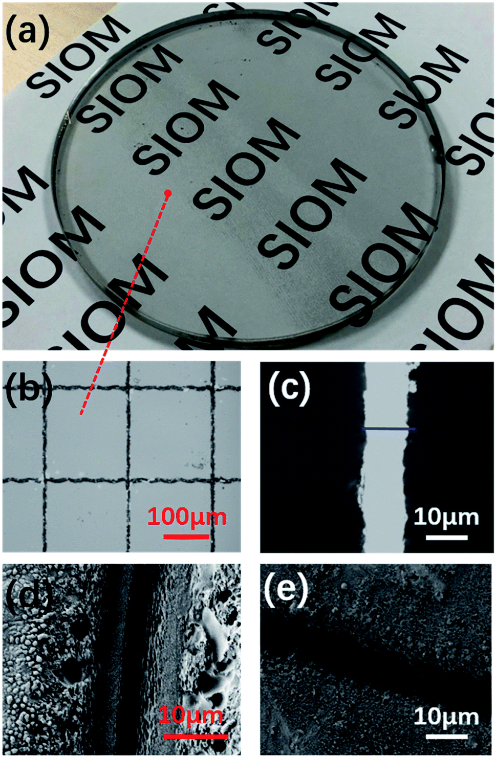 | ||
| Fig. 5 (a) Demonstration of the transparency of the double-layer metal mesh laid over a photograph. (b and c) Micrographs of the metal mesh and the line width of the mesh, respectively. The SEM images of the grooved structure sculptured by femtosecond laser on (d) the photoresist and (e) the quartz glass. | ||
Visible transmittance of the window was measured with a UV/VIS/NIR spectrometer (Lambda 750) at wavelength of 400–900 nm. The normal visible transmittance of the quartz glass, monolayer mesh and double-layer mesh (same period and line width) are depicted in Fig. 6. The quartz glass exhibits an intrinsic average visible transmittance of 93.21% at 400–900 nm. Meanwhile, the average measured transmittance of the double-layer mesh is 76.35%, which is approximately 9.38% less than that of single layer mesh (85.73%), indicating good optical transmission performance.
 | ||
| Fig. 6 Normalized optical transmittance of quartz glass, monolayer metal mesh and double-layer metal mesh from 400 nm to 900 nm. | ||
The EMI SE was obtained by a measurement system composed of a vector network analyzer (Agilent N5230A), a transmitting antenna, and a receiving antenna. The receiving antenna is installed in the microwave anechoic chamber, the sample was placed on a perforated metal plate between transmitting and receiving antenna, as illustrated in Fig. 7(a). The systems was calibrated without the sample before the test. Fig. 7(b) presents the simulated and measured EMI SE of monolayer and double-layer mesh from 150 MHz to 5 GHz. The monolayer mesh exhibits the measured SE of 19.74–48.34 dB. Moreover, the double-layer mesh demonstrates excellent shielding performance that the SE is over 37.61 dB from 150 MHz to 5 GHz, with a maximal SE of 75.84 dB at 3.58 GHz. The SE of double-layer is increased by 26.79 dB (99.80% energy attenuation) at 150 MHz and 10.91 dB (91.89% energy attenuation) at 5 GHz, compared with that of the monolayer mesh. The simulated SE of the monolayer mesh are higher than the measured ones at low frequency, while they are in good agreement as the frequency is further increased. However, the simulated result of the double-layer mesh is slightly higher the experimental result in the whole frequency band. The error is owing to inhomogeneous thickness of metal film, inhomogeneous the linewidth of the mesh, and the electrical conductivity of the evaporated metal film in the measurement is different from that of the simulated condition. In addition, another important reason is the error of the SE measurement system. The tested wavelength at low frequency is larger than the size of the sample, the perforated metal plate used to place the sample has a certain deviation as a reference. In the practical experiment, when the SE of the double-layer mesh reaches over 50 dB, the transmittance is only 0.00001, and the small chinks between the sample and the metal plate will also cause a significant impact on the SE. The enhanced SE of double-layer mesh resulted from the multiple reflections between the two mesh layers, which increased the reflectivity and dissipation of incident wave. Further, the Ni–Au composite mesh realizes the transition of shielding performance from megahertz frequency to gigahertz frequency.
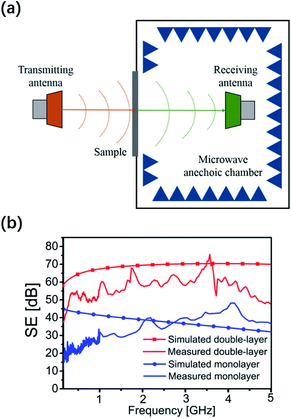 | ||
| Fig. 7 (a) Schematic diagram for measuring the SE of fabricated samples, (b) experimental and simulated results of double-layer and monolayer mesh. | ||
Conclusions
In conclusion, we developed and manufactured an excellent Au–Ni composite mesh for transparent EMI shielding window. Moreover, the window simultaneously achieves strong microwave shielding performance and high optical transmittance. Numerical simulation shows that the EMI SE of the double-layer mesh is obviously enhanced by increasing the thickness of substrate in the low frequency range far below the first interfere valley. The experimental results demonstrated that the window can yield the SE greater than 37.61 dB from 150 MHz to 5 GHz, with a maximal SE of 75.84 dB at 3.58 GHz, and an average normalized optical transmittance of ∼76.35% at 400–900 nm. In addition, femtosecond laser direct writing processing technology is used to manufacture double-layer metal grids, ensuring that the fabricated grids have excellent firmness, wear resistance and durability. These outstanding properties make the double-layer mesh a powerful structure for EMI shielding windows, as well as potential application in the precision monitoring devices.Conflicts of interest
There are no conflicts to declare.Acknowledgements
National Natural Science Foundation of China (NSFC) (61675219, 61875256). Hongxing Dong acknowledges the Youth Top-notch Talent Support Program in Shanghai, Shanghai Rising-star Program and Shanghai Sailing Program (18YF1426300).References
- X. Ma, B. Shen, L. Zhang, Y. Liu, W. Zhai and W. Zheng, Compos. Sci. Technol., 2018, 158, 86–93 CrossRef CAS.
- L. Ma, Z. Lu, J. Tan, X. Ding, N. Black, T. Li, J. Gallop and L. Hao, ACS Appl. Mater. Interfaces, 2017, 9(39), 34221–34229 CrossRef CAS.
- Y. Han, Y. Liu, L. Han, J. Lin and P. Jin, Carbon, 2017, 115, 34–42 CrossRef CAS.
- J. Jung, H. Lee, I. Ha, H. Cho, K. K. Kim, J. Kwon, P. Won, S. Hong and S. H. Ko, ACS Appl. Mater. Interfaces, 2017, 9(51), 44609–44616 CrossRef CAS.
- R. Kumar, H. K. Choudhary, S. P. Pawar, S. Bose and B. Sahoo, Phys. Chem. Chem. Phys., 2017, 19(34), 23268–23279 RSC.
- Z. Lu, L. Ma, J. Tan, H. Wang and X. Ding, Nanoscale, 2016, 8(37), 16684–16693 RSC.
- D. G. Kim, J. H. Choi, D. K. Choi and S. W. Kim, ACS Appl. Mater. Interfaces, 2018, 10(35), 29730–29740 CrossRef CAS.
- M. Cao, C. Han, X. Wang, M. Zhang, Y. Zhang, J. Yang, X. Fang and J. Yuan, J. Mater. Chem. C, 2018, 6(17), 4586–4602 RSC.
- L.-C. Jia, D.-X. Yan, X. Liu, R. Ma, H.-Y. Wu and Z.-M. Li, ACS Appl. Mater. Interfaces, 2018, 10(14), 11941–11949 CrossRef CAS.
- K. Sabira, M. P. Jayakrishnan, P. Saheeda and S. Jayalekshmi, Eur. Polym. J., 2018, 99, 437–444 CrossRef CAS.
- D.-H. Kim, Y. Kim and J.-W. Kim, Mater. Des., 2016, 89, 703–707 CrossRef CAS.
- Y. Han, J. Lin, Y. Liu, H. Fu, Y. Ma, P. Jin and J. Tan, Sci. Rep., 2016, 6, 25601 CrossRef CAS.
- Z. Lu, Y. Liu, H. Wang, Y. Zhang and J. Tan, Opt. Express, 2016, 24(23), 26109–26118 CrossRef.
- Z. Chen, C. Xu, C. Ma, W. Ren and H.-M. Cheng, Adv. Mater., 2013, 25(9), 1296–1300 CrossRef CAS.
- P. Kumar, P. V. Reddy, B. Choudhury, P. Chowdhury and H. C. Barshilia, Thin Solid Films, 2016, 612, 350–357 CrossRef CAS.
- D. Angmo, T. T. Larsen-Olsen, M. Jørgensen, R. R. Søndergaard and F. C. Krebs, Adv. Energy Mater., 2013, 3(2), 172–175 CrossRef CAS.
- J. Tan and Z. Lu, Opt. Express, 2007, 15(3), 790–796 CrossRef.
- Z. Lu, H. Wang, T. Tan and S. Lin, Appl. Phys. Lett., 2014, 105(24), 241904 CrossRef.
- H. Wang, Z. Lu, Y. Liu, J. Tan, L. Ma and S. Lin, Opt. Lett., 2017, 42(8), 1620–1623 CrossRef CAS.
- Z. Lu, L. Ma, J. Tan, H. Wang and X. Ding, 2D Mater., 2017, 4(2), 025021 CrossRef.
- Z. Lu, L. Ma, J. Tan, H. Wang and X. Ding, Nanoscale, 2016, 8(37), 16684–16693 RSC.
- F. Sima, K. Sugioka, R. M. Vázquez, R. Osellame, L. Kelemen and P. Ormos, Nanophotonics, 2018, 7(3), 613–634 CAS.
- X. Sun, D. Cui, Y. Hu, D. Chu, G. Chen, J. Yu, J. Zhou and J. Duan, Chin. Opt. Lett., 2018, 16(10), 101402 CrossRef.
- J. Lin, Y. Xu, Z. Fang, M. Wang, J. Song, N. Wang, L. Qiao, W. Fang and Y. Cheng, Sci. Rep., 2015, 5, 8072 CrossRef CAS.
- Y. Lin, J. Han, M. Cai, W. Liu, X. Luo, H. Zhang and M. Zhong, J. Mater. Chem. A, 2018, 6(19), 9049–9056 RSC.
- D. Tan, K. N. Sharafudeen, Y. Yue and J. Qiu, Prog. Mater. Sci., 2016, 76, 154–228 CrossRef.
- J. Hernandez-Rueda, N. W. Troy, P. Freudenberger, R. K. Brow and D. M. Krol, Opt. Mater. Express, 2018, 8(12), 3622–3634 CrossRef.
- J. Xu, X. Li, Y. Zhong, Z. Wang, Z. Chai, W. Li, C. Jing and Y. Cheng, Adv. Mater. Technol., 2018, 3(12), 1800372 CrossRef.
- S. Maiti, N. K. Shrivastava, S. Suin and B. B. Khatua, ACS Appl. Mater. Interfaces, 2013, 5(11), 4712–4724 CrossRef CAS.
- S. Kim, J.-S. Oh, M.-G. Kim, W. Jang, M. Wang, Y. Kim, H. W. Seo, Y. C. Kim, J.-H. Lee, Y. Lee and J.-D. Nam, ACS Appl. Mater. Interfaces, 2014, 6(20), 17647–17653 CrossRef CAS.
Footnote |
| † Electronic supplementary information (ESI) available. See DOI: 10.1039/c9ra03519b |
| This journal is © The Royal Society of Chemistry 2019 |