DOI:
10.1039/C9RA03483H
(Paper)
RSC Adv., 2019,
9, 23774-23779
Fabrication and sensing application of a silver nanoshell array structure by a micro-flow injection method
Received
9th May 2019
, Accepted 11th July 2019
First published on 31st July 2019
Abstract
A two-dimensional periodic metallic spherical shell array structure with controllable geometric parameters was fabricated on the target substrate by microsphere templating and magnetron sputtering. The micro-flow injection method was used to prepare a two-dimensional colloidal microsphere template, and reactive ion etching (RIE) was used to change the spherical spacing. The geometric parameters and spectral characteristics of the spherical shell array structure were analyzed with the simulation software FDTD solutions. The nanostructural morphology and optical properties of the samples were characterized by scanning electron microscopy (SEM) and optical spectral analysis (OSA). The refractive index sensing application based on the principle of the local surface plasmon resonance (LSPR) and plasmonic interference was realized. The results show that the spherical shell arrays structure is sensitive to the surrounding environment, the refractive index sensitivity of spherical shell array structure is 527.07 nm per RIU and 922.25 nm per RIU, and the quality factor FOM is 16.5 and 15.3, respectively. The techniques demonstrated can produce large-area periodic nanostructure arrays with ultra-large production in cost-competitive ways. In addition, these properties make them applicable to multiple applications, such as surface plasmon sensors and various optical device.
1 Introduction
Metal Nano array structures are widely used in physical, chemical and biomedicine parameters sensing due to their characteristic local surface plasmon resonance (LSPR).1,2 Among various metal nano array structures, the spherical shell structure has attracted more attention because of its relatively simple preparation and wide tuning range of LSPR wavelength.3–7 It is shown that the LSPR resonance peak can be changed by varying the shape, size, spacing and surrounding environment of the nanoparticles on the liquid, silicon or glass substrates.8–12 In recent years, considerable progress has been made in the preparation and application of metal nanospheres.13–17 Liu18 and Zhou19 have prepared gold nanoparticles. Hirsch and other20,21 have obtained core and shell structures of SiO2 and Au, which have been applied to thermal ablation therapy and rapid whole blood immunoassay for cancer cells. Actually, polystyrene (PS) spheres can be used to obtain large-area periodically regular arrays template which can control dimension.22 Colloidal assemblies are used as templates for etching or deposition of materials, which represents a cost-effective and simple route for surface patterning and fabrication of ordered arrays compared to serial direct writing techniques such as electron beam lithography.
In this paper, large area two-dimensional colloidal microsphere templates were fabricated by a microfluidic injection method, and silver nanoshells with controllable geometric parameters on the target substrate were obtained by sputtering and reactive ion etching (RIE). The optical properties with different etching times and different silver film thickness were investigated by FDTD simulation and experiment analysis.
It is found that the spectral characteristics of the structure are not only related to the structural parameters, but also related to the refractive index of the filling material in the micro-slit inside the structure. The silver nanoshell structure is sensitive to the surrounding environment originating from surface plasmon resonance and plasmon interference effect, and the refractive index test showed that the structural refractive index sensitivity was 527.07 nm per RIU and 922.25 nm per RIU, and the quality factor FOM was 16.5 and 15.3, respectively.
2 Fabrication and experiment
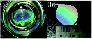
As shown in Fig. 1, the preparation of two-dimensional colloidal crystal monolayer with hexagonal close packing on the gas–liquid surface by microfluidic injection method. A small amount of sodium dodecyl sulfate (SDS) solution is added to ensure the quality of the monolayer before transferred to the target substrate. Combined with the physical processing method, the two-dimensional periodic spherical shell array structure is completed.
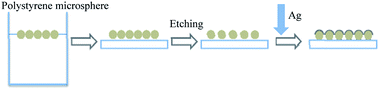 |
| | Fig. 1 Preparation of flow chart. | |
2.1 Method
Detailed process: (1) cleaning: the beaker used in the experiment, the substrate was cleaned with acetone, anhydrous ethanol ultrasonic cleaning, substrate treated with clean water; (2) micro-flow injection: the target suspension was prepared in proportion of the original solution of 690 nm polystyrene microspheres and the dispersion solution (ethanol, n-butanol), and the target suspension was dispersed by ultrasound for 15 min. The two-dimensional colloidal microspheres template was prepared on the gas–liquid surface by micro-flow injection method. And transfer to the substrate as shown in Fig. 2; (3) etching: the reaction ion (RIE) etching was carried out with O2 as the reaction gas and PS microsphere template to change the spacing of metal spherical shell array indirectly. The etching parameters were RF power 50 W, reaction pressure 0.1 Pa, etching time 120 s, and the etching time was 120 s, and the etching parameters were RF power 50 W, reaction pressure 0.1 Pa, and etching time 120 s. (4) Deposition of metal films: silver films were deposited on etched samples by vacuum magnetron sputtering, and the metal spherical shells array with the film thickness of 10 nm was obtained.
 |
| | Fig. 2 Preparation of monolayer of gas–liquid surface: (a) gas–liquid surface assembly diagram; (b) transfer completion diagram.23 | |
2.2 Characterization
The two-dimensional colloidal photonic crystal samples were observed under optical microscope, which has larger area and better order. The scanning electron microscopy (SEM) pictures of the fabricated device are shown in Fig. 3. As shown in Fig. 3(a) and (b), the colloidal microspheres have good quality and can be used as templates for micro-nano structures. From the electron microscopy of the spherical shell array [Fig. 3(c) and (d)], it can be seen that the metal sphere shell array formed by RIE etching and magnetron sputtering deposition of metal film is basically formed. The metallic silver film covers only the upper hemispheres of the microspheres, and the quality is consistent and uniform.
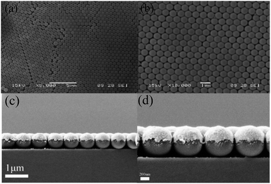 |
| | Fig. 3 Two-dimensional microstructural electron microscopy: (a and b) two-dimensional colloidal crystals of 2 min etched by 690 nm; (c and d) two-dimensional metal spherical shell arrays of 2 min etched by 690 nm with 10 nm silver film. | |
3 Results and application
3.1 Spectral analysis
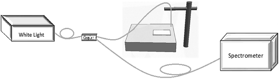
The test system is built with AQ4305 white light source, 50![[thin space (1/6-em)]](https://www.rsc.org/images/entities/char_2009.gif) :50 1 × 2 coupler and ocean spectrum analyzer. As shown in Fig. 4, the reflection spectrum of metal spherical shell array is obtained experimentally. The spectrum range of white light source is 400–1800 nm, and the coupler is connected with white light source, spectrum analyzer and multi-mode fiber respectively. The light of light source is vertically incident from the end of multi-mode fiber onto the 690 nm two-dimensional metal spherical shell array which etched by RIE for 2 minutes and magnetron sputtering 10 nm silver film. The source is reflected back into the optical fiber, coupled into the spectrum analyzer, and the spectra are measured.
:50 1 × 2 coupler and ocean spectrum analyzer. As shown in Fig. 4, the reflection spectrum of metal spherical shell array is obtained experimentally. The spectrum range of white light source is 400–1800 nm, and the coupler is connected with white light source, spectrum analyzer and multi-mode fiber respectively. The light of light source is vertically incident from the end of multi-mode fiber onto the 690 nm two-dimensional metal spherical shell array which etched by RIE for 2 minutes and magnetron sputtering 10 nm silver film. The source is reflected back into the optical fiber, coupled into the spectrum analyzer, and the spectra are measured.
 |
| | Fig. 4 Measurement system diagram. | |
The reflection spectra and tunable mechanism of the two-dimensional periodic metal spherical shell array are shown in Fig. 5. As can be seen from the Fig. 5(a), there are several peaks and valleys in the spectrum. This is due to the incident light of the light source onto the nanoshell arrays and the surface plasma wave induced by the metal spherical shell array, which, in addition to generating resonance, propagates horizontally at the interface of the metal spherical shell, as shown in Fig. 5(b). Finally , the multi-reflection plasma interference is generated at the boundary of the finite-size mode. It is because of the sensitivity of local surface plasmon resonance (LSPR) and plasmon interference to refractive index that the real time measurement can be realized and it is of great significance in many biosensors.
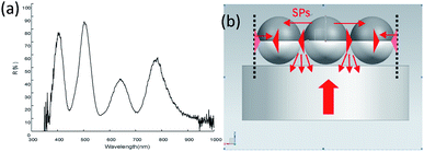 |
| | Fig. 5 Spectrum and principle: (a) sample reflectance spectroscopy; (b) tunable mechanism diagram.24,25 | |
3.2 Simulation analysis
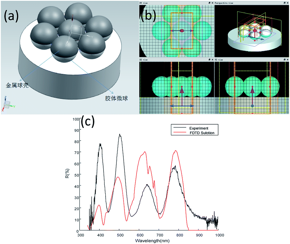
The FDTD solutions (Lumerical FDTD Solutions) is used to simulate the spectral characteristics of the nanoshell arrays, as shown in Fig. 6. Here, in order to improve the calculation efficiency, we set the X-, Y-axis to the periodic boundary condition, and the Z-axis to perfectly matched layer (PML) to ensure the continuity of the boundary dielectric. In theory, the λ/10 mesh will have a more reliable accuracy. Save the running time of the calculation and the memory required for the operation under the condition of ensuring the accuracy of the calculation, so the model mesh size is set to 4 nm. The number and location of measured resonance peaks are apparent, which agree well with the numerical simulation. The deviation is about 5–10 nm. The error may be due to the difference between the specific experimental structure and the simulation model, such as the thickness of the metal spherical shell, the size of the colloid sphere, the distance between the spherical shells.
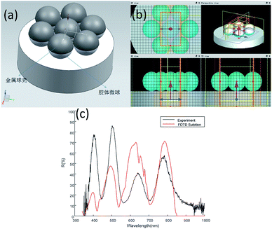 |
| | Fig. 6 Simulation and experiment of colloid microsphere/metal spherical shell structure: (a) model; (b) simulation interface diagram of FDTD solutions; (c) comparison diagram of simulation and experimental spectra. | |
3.3 Experimental results of nanoshell with varied etching time and Ag film thickness
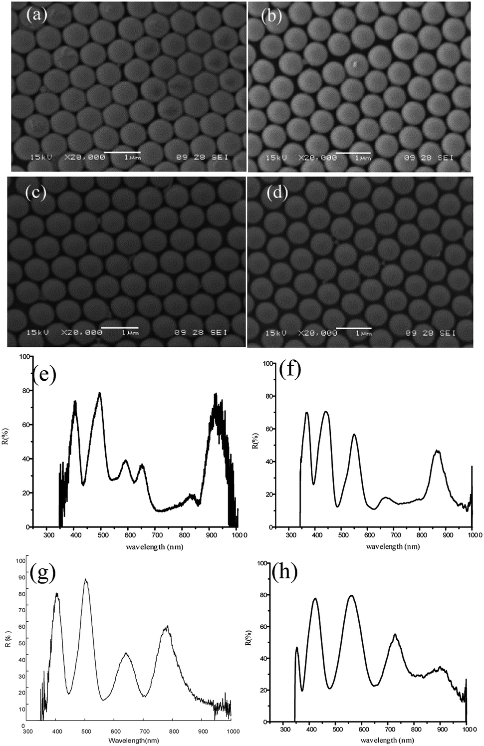
3.3.1 Etching time. In the experiment, the template of 690 nm single-layer PS microspheres array is prepared by RIE etching. The etching time determines the spacing of the colloidal microsphere template, which in turn affects the spacing of the nanoshell. As shown in Fig. 7, for the 690 nm polystyrene colloidal microsphere array, the colloidal spheres are arranged orderly when there is no RIE etching. From the scanning electron microscope Fig. 7(a–d), the size and spacing of colloidal microspheres can be clearly observed. When the oxygen ion etching time are 0, 60, 120 and 180 s, the diameter of the microspheres becomes 690, 670, 640 and 610 nm, respectively. When the etching time is gradually increased, the spacing of the PS microspheres increases with the increase of the time. From the reflectance spectra Fig. 7(e–h), we can see that the size of the structure spacing can affect the position and quality of the spectra , wherein the peak trough contrast of the spectra graph at the time of the etching 120 s is the largest, so that the sensing effect is the best.
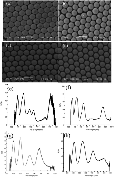 |
| | Fig. 7 SME image of template with different etching time and corresponding spectra of spherical shell: (a–d) SEM of 690 nm polystyrene microsphere template under etching time of t = 0, 60, 120 and 180 s; (e–h) reflection spectra with Ag film thickness 10 nm. | |
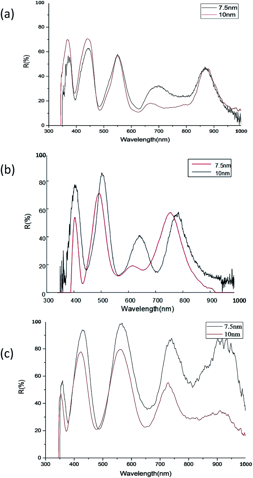
3.3.2 Ag film thickness. The film thickness of the metal shell is determined by the time of the vacuum magnetron sputtering directly, nevertheless, the result of the resonance effect is unsatisfactory when the film is too thick or too thin. The spectra of metal shell with films thickness 7.5 and 10 nm are discussed below, as shown in Fig. 8. In contrast, the position of the peak in the spectra varied with the film thickness. When the thickness of the metal film is increased from 7.5 nm to 10 nm, the contrast of the wave peak and valley of spectrum is more obvious. In the comparison of the above results, the effect of the silver film 10 nm after RIE etching 2 minutes is the best.
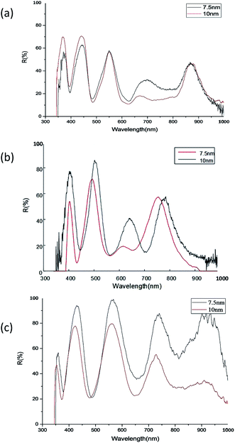 |
| | Fig. 8 Spectrogram of 7.5, 10 nm metal spherical shell: (a) RIE etching 60 s; (b) RIE etching 120 s; (c) RIE etching 180 s. | |
3.4 Sensing experiment
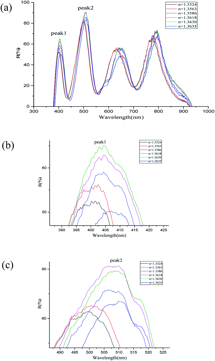
The multimode optical fiber is used to contact the light source to the nanoshell array and the signals reflected from the structure are received by spectrometer. The signals carrying the environment change are introduced into the spectrum analyzer. The relationship between the spectrum and the refractive index of the environment is obtained by observing the shift of the spectrum, thus the change of the refractive index in the environment is obtained. In the experiments, a mixed solution of ethanol and water with different concentration gradients was added to the structure of the metal spherical shell respectively for obtaining the result by spectrometer [Fig. 9]. By changing the concentration of the solution to 30%, 40%, 50%, 60%, 70%, 80%, the refractive index of the solution was tuned to 1.3524, 1.3563, 1.3586, 1.3618, 1.3630, 1.3635, respectively. The refractive index of the solution was calibrated by using Abbe refractive index in advance.
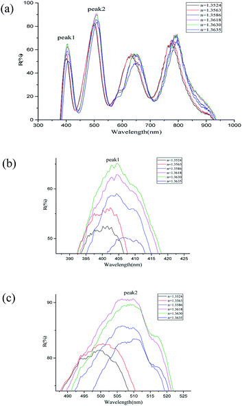 |
| | Fig. 9 Refractive index migration spectrum: (a) holistic spectrogram; (b) wave peak 1; (c) wave peak 2. | |
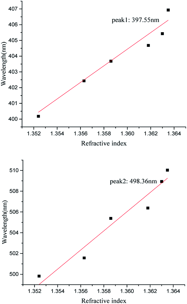
From Fig. 9, it is known that the reflected spectra offset a significant change with the change of the refractive index of the solution. The interference intensity of at different peaks and valleys is enhanced or weakened. The spectral lines are shifted as a whole with the increase of the refractive index26,27 of the medium. The wavelength positions of the wave peak 1 and wave peak 2 are recorded with the refractive index. The shift of the original data is used to synthesize the sensing curve. As shown in Fig. 10, the spectral line basically shows a linear relationship. Based on the linear relationship between the refractive index and the position of the wave peak, the refractive index of the medium can be obtained by measuring the shift of the interference wave peak, thus realizing the refractive index sensing. According to the formula of sensitivity calculation S = S = Δλ/Δn, where Δλ is the corresponding central wavelength shift of the resonant dips and Δn is the difference of the refractive index, the refractive index sensitivity of wave peak 1 and wave peak 2 is calculated to be 527.07 nm per RIU and 922.25 nm per RIU respectively. FOM (Figure of Merit) can be defined as the relationship between the sensitivity and the half-height width of the resonant wave, expressed as FOM = S/FWHM, FOM is 16.5 and 15.3 respectively. Compared with the refractive index sensitivity of the two-dimensional nano-hole array structure that has been reported 220 nm per RIU,28 the two-dimensional nanoshell array's sensing performance is more sensitive.
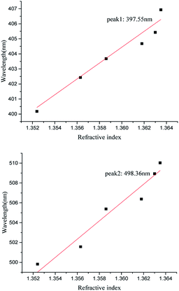 |
| | Fig. 10 The fitting curve of peak 1 and peak 2. | |
4. Conclusions
In conclusion, a plasmonic interferometer with nanoshell array structure has been successfully demonstrated for refractive index sensing. The two-dimension periodic metal spherical nanoshell array structure was prepared by the method of combining the gas liquid surface micro-flow injection and etching, and the spectral properties of the structural samples were measured and analyzed. The influences of two different mechanisms (i.e., LSPR and plasmonic interference) on the reflection spectrum have been studied and utilized as a novel physical mechanism for refractive index sensing on a miniaturized sensing area. The refractive index sensitivity can reach 527.27 nm per RIU and 922.25 nm per RIU, and FOM is 16.5 and 15.3 respectively. Next, the effects of etching time and thickness of deposited metal film on the preparation of two-dimensional periodic metallic nanoshell are discussed by comparing different results. The method and experimental installation used in the experiment are simplicity. Combined with different sensitive materials, it can be applied to many aspects of chemical and biological sensing.
Conflicts of interest
The authors declare no conflict of interest.
Acknowledgements
Project supported by the National Natural Science Foundation of China (Grant No. 51775283), the Natural Science Foundation of Jiangsu Province, China (Grant No. BK20161559).
Notes and references
- K. A. Willets and R. P. Van Duyne, Annu. Rev. Phys. Chem., 2007, 58(1), 267–297 CrossRef CAS.
- F. Li, X. G. Luo, S. L. Zhu, C. L. Du and Q. L. Deng, Precis. Eng., 2007, 5(2), 121–124 CAS.
- J. R. Cole and N. J. Halas, Appl. Phys. Lett., 2006, 89(89), 153120 CrossRef.
- Y. M. Bai, J. Wang, N. F. Chen, J. X. Yao, X. W. Zhang, Z. G. Yin, H. Zhang and T. M. Huang, Chin. Phys. Lett., 2011, 28(8), 087306 CrossRef.
- D. J. Wu and X. J. Liu, Appl. Phys. Lett., 2010, 97(6), 1904 CrossRef.
- C. H. Liu and B. Q. Li, J. Phys. Chem. C, 2011, 115(13), 5323–5333 CrossRef CAS.
- H. X. Zhang, Y. Gu and Q. H. Gong, Chin. Phys. B, 2008, 17(7), 2567–2573 CrossRef.
- X. F. Zhang and X. Yan, Acta Phys. Sin., 2013, 62(3), 037805 Search PubMed.
- T. R. Jensen, M. D. Malinsky and C. L. Haynes, J. Phys. Chem. B, 2000, 104(45), 10549–10556 CrossRef CAS.
- W. C. Lin, L. S. Liao, Y. H. Chen, H. C. Chang, D. P. Tsai and H. P. Chiang, Plasmonics, 2011, 6(2), 201–206 CrossRef CAS.
- Y. F. Chau and Z. H. Jiang, Plasmonics, 2011, 6(3), 581–589 CrossRef CAS.
- W. Yang, Y. F. Chou Chau and S. C. Jheng, Phys. Plasmas, 2013, 20(6), 064503 CrossRef.
- A. J. Haes and R. P. van Duyne, Expert Rev. Mol. Diagn., 2004, 4, 527–537 CrossRef CAS PubMed.
- R. A. Alvarez-Puebla, D. J. Ross, G. A. Nazri and R. F. Aroca, Langmuir, 2005, 21(23), 10504–10508 CrossRef CAS PubMed.
- D. P. O'Neal, L. R. Hirsch, N. J. Halas, J. D. Paynea and J. L. West, Cancer Lett., 2004, 209(2), 171–176 CrossRef PubMed.
- H. B. Ni, L. Ge, X. Liu, Y. Zhou, J. H. Chang, H. Ali, C. Pan, T. T. Wang and M. Wang, RSC Adv., 2018, 8, 39735 RSC.
- D. J. Wu and X. J. Liu, Acta Phys. Sin., 2008, 57, 5138 CAS.
- Z. X. Liu, H. W. Song, L. X. Yu and L. Yang, Appl. Phys. Lett., 2005, 86, 113109 CrossRef.
- S. Zhou, H. S. I. Honma and H. Komiyama, Phys. Rev. B: Condens. Matter Mater. Phys., 1994, 50, 12052–12056 CrossRef PubMed.
- L. R. Hirsch, J. B. Jackson, A. Lee, N. J. Halas and J. L. West, Anal. Chem., 2003, 75(10), 2377–2381 CrossRef CAS PubMed.
- L. R. Hirsch, R. J. Stafford, J. A. Bankson, S. R. Sershen, B. Rivera, R. E. Price, J. D. Hazle, N. J. Halas and J. L. West, Proc. Natl. Acad. Sci. U. S. A., 2003, 100(23), 13549–13554 CrossRef CAS PubMed.
- L. M. Zhang, Y. L. Liao, Q. F. Fan, J. Cao and Q. H. Mao, Precis. Eng., 2012, 10(4), 302–305 CAS.
- C. S. Deng, T. T. Pan, L. Du, M. Wang, H. B. Ni and X. Q. Ni, Chem. Res. Chin. Univ., 2018, 39(4), 708–713 CAS.
- Y. F. Chau, Plasmonics, 2009, 4, 253–259 CrossRef CAS.
- Y. F. Chau, Z. H. Jiang, H. Y. Li, G. M. Lin, F. L. Wu and W. H. Lin, Progress In Electromagnetics Research B, 2011, 28, 183–199 CrossRef.
- Y. F. Chou Chau, C. T. Chou Chao, H. P. Chiang, Ch. M. Lim, N. Y. Voo and A. H. Mahadi, J. Nanopart. Res., 2018, 20, 190 CrossRef.
- Y. F. Chau, C. T. Chou Chao, C. M. Lim, H. J. Huang and H. P. Chiang, ACS Omega, 2018, 3(7), 7508–7516 CrossRef CAS.
- Z. J. Zhang, Y. Y. Chen, H. J. Liu, H. Bae, D. A. Olson, A. K. Gupta and M. Yu, Opt. Express, 2015, 23(8), 10732–10740 CrossRef CAS PubMed.
|
| This journal is © The Royal Society of Chemistry 2019 |
Click here to see how this site uses Cookies. View our privacy policy here. 
 Open Access Article
 This Open Access Article is licensed under a Creative Commons Attribution-Non Commercial 3.0 Unported Licence
 ,
Cai Song Deng,
Ting Ting Pan,
Hui Hao and
Ming Wang*
,
Cai Song Deng,
Ting Ting Pan,
Hui Hao and
Ming Wang*