DOI:
10.1039/C9RA03383A
(Paper)
RSC Adv., 2019,
9, 23785-23790
Study on the synthesis of β-SiC nanoparticles from diamond-wire silicon cutting waste
Received
6th May 2019
, Accepted 8th July 2019
First published on 31st July 2019
Abstract
Large amounts of silicon have been wasted as silicon cutting waste (SCW) during the silicon wafer production process, which increases the cost of photovoltaic solar cells and causes environmental pollution. In this paper, an innovative approach for producing β-SiC nanoparticles by using SCW as silicon source and sucrose as carbon source is reported. The synthesized β-SiC nanoparticles were characterized by XRD, FTIR, SEM, TEM, Raman, PL and DSC. The results showed that β-SiC nanoparticles were successfully prepared with a particle size ranging from 40 to 50 nm, and have special photoluminescence as well as good thermal stability. The recycling of SCW can not only solve the environmental pollution issue but also benefits the economy.
1. Introduction
With the rapid development of the worldwide photovoltaic industry, the demand for crystalline silicon wafers is on the rise.1 Silicon wafers are produced from crystalline silicon ingots by multi-wire slicing methods. There are basically two methods for silicon ingots slicing.2 The early conventional method is called the mortar process, in which silicon ingots are sliced by abrasive particles (SiC) adhered on the wire and suspended in an organic coolant (glycol). The other alternative method is called the diamond-wire sawing method, where silicon ingots are sliced by a high-speed reciprocating wire coated with diamond. Currently, the latter method has become the main method of silicon ingot slicing for its many advantages, such as high slicing efficiency and high-quality products. However, whatever the slicing method, approximately 35–40% crystalline silicon would be wasted as silicon cutting waste (SCW) during the wafer producing process since the diameter of the slicing wire is nearly equal to the thickness of silicon wafers.3,4
To date, a lot of studies have been devoted to separating high purity silicon from the SCW. The proposed works contain phase-transfer separation,5 centrifugation,6 laser-assisted vacuum smelting,7 hydrobromination,8 slag refining and alloying process.9,10 However, most of these studies are limited to the laboratory stage and the recovery scale is small. Therefore, it is necessary to explore an efficient, economic and feasible way to recycle the SCW for preparing high value-added products. Since part of silicon particles are oxidized in the slicing process, a cover of SiO2 film would be generated on the surface of silicon particles.11 Therefore, the SCW is a potential raw material for producing silicon carbide as its main constituents are Si and small amounts of SiO2.
SiC has outstanding physical and chemical thermal stability, excellent radiation resistance and mechanical properties, high thermal conductivity and wide band gap (2.4 eV for 3C–SiC).12,13 Hence the nanostructured SiC materials has been applied in the filed nanoscale electro-devices, nanosensors, biological labels and functional ceramic.14–16 The reported routes for producing SiC nanoparticles include carbon thermal reduction method,17 template growth method,18 arc discharge method,19 chemical vapor deposition method,20 sol–gel method21,22 and microwave assisted method.23 Besides, a lot of efforts have also been devoted to the synthesis of SiC nanocrystals with different waste. Rajagopal et al.24 synthesized valuable SiC-glass fiber composite from waste printed circuit boards and compact discs. Rajarao et al.15 used electronic waste as carbon source to produce SiC-nanoparticles with a size of 40–90 nm. Zhicheng Ju et al.25 reported the synthesis of 3C–SiC nanomaterials utilizing waste plastics and Si powder at 350–500 °C in a stainless steel autoclave. Maroufi et al.26 succeeded in preparing mesoporous SiC nanofiber/particle composite with e-waste glass and waste tyre rubber in a high-temperature tubular furnace.
In this study, we successfully prepare 3C–SiC nanoparticle using the SCW and sucrose as the raw materials. The properties of synthesized SiC nanoparticle have been investigated in detail. It was found that the produced 3C–SiC nanoparticle has the properties of special photoluminescence and good thermal stability. This method can be a feasible and economical route to produce SiC nanoparticle and reduce the environmental pollution of SCW.
2 Experimental
2.1 Raw materials
SCW and sucrose were used as the raw materials in this paper. The SCW was provided by a new energy company in China. Sucrose and other reagents used in this paper were analytically pure and purchased from Sinopharm Chemical Reagent Co., Ltd. in Shenyang of China.
2.2 Methods
Firstly, sucrose was dissolved in deionized water in a beaker. Then, SCW was put into sucrose solution and stirred vigorously to form a homogeneous suspension (the mass ratio of SCW to sucrose was set as 1![[thin space (1/6-em)]](https://www.rsc.org/images/entities/char_2009.gif) :1). The suspension was continued heated at 100 °C until the deionized water completely evaporated. Subsequently, a dry black solid obtained and was ground into powder. After above mentioned procedure, the two raw materials became a uniform mixture of silicon and carbon sources. The mixture was placed in an alumina crucible and heated at 1500 °C with a tube furnace in a flowing argon atmosphere. The heating rate was 5 °C min−1 and the holding time at 1500 °C was 2 h. Ar gas was kept on following until the furnace was cooled to room temperature, the as-synthesized products were collected and then purified by diluted HF solution. The purified products were washed by deionized water to neutral and dried in an oven.
:1). The suspension was continued heated at 100 °C until the deionized water completely evaporated. Subsequently, a dry black solid obtained and was ground into powder. After above mentioned procedure, the two raw materials became a uniform mixture of silicon and carbon sources. The mixture was placed in an alumina crucible and heated at 1500 °C with a tube furnace in a flowing argon atmosphere. The heating rate was 5 °C min−1 and the holding time at 1500 °C was 2 h. Ar gas was kept on following until the furnace was cooled to room temperature, the as-synthesized products were collected and then purified by diluted HF solution. The purified products were washed by deionized water to neutral and dried in an oven.
2.3 Analysis
The X-ray diffraction (XRD, PANalytical X'Pert diffractometer with Cu-Kα radiation (ƛ = 0.15406 nm)) was used to identify the phase component of the products. The infrared (IR) spectrum (Nicolet 6700 Fourier transform infrared spectrometer) was performed to study the surface chemistry of the products in the wavenumber range of 4000–400 cm−1. The field emission scanning electron microscopy (SEM, ULTRA PLUS, Zeiss Germany) and transmission electron microscopy (TEM, FEI Tecnai G2 F20) with selected area electro diffraction pattern were used to investigate the morphology and structure of the products. The Raman spectra (Renishaw Invia microscope system) was used to study the crystallinity and molecular structure of the products with a wavelength of 514.5 nm excitation from an argon ion laser source at room temperature. The fluorescence spectrophotometer with a Xe lamp (Hitachi 850) was used to measure the photoluminescence (PL) spectra of the products at room temperature. The thermal analyzer apparatus (Netzsch TGA/STA449F3) was used to study the thermal gravimetric and differential scanning calorimetry analysis of the products under air flow.
3. Results and discussion
Fig. 1(a) shows the typical SEM image and the EDS analysis of the SCW. It can be seen that the particles of the SCW are in a scaly shape and its size is mainly micron order. The EDS patterns in the bottom left corner of Fig. 1(a) show that the SCW is consisted of elements of Si and O. The presence of O element in the SCW is mainly due to the oxidation of the silicon particles during the slicing process. This is because that the fine particle size and large specific surface area of SCW, it is easy to be oxidized. The particle size distribution of the SCW was shown in Fig. 2(a). It is observed that the particle size of the SCW is of micron grade with a mean diameter of ∼1.34 μm, which is in correspondence with the result of SEM image. We all know that diamond cutting waste is mainly composed of silicon and silicon oxide. Also it can be obtained from the XRD analysis results below. To determine the exact content of each composition of the SCW, a further chemical analysis was performed and the result is illustrated in Table 1, it is shown that the SCW is basically composed of 79.80 wt% Si, 15.40 wt% SiO2, 2.10 wt% C and 2.70 wt% metallic impurities. Moreover, the content of C is derived from the abrasion of diamond during the slicing process. As mentioned above, the high purity, fine particle size and high activity of SCW are very suitable for preparing nano-SiC.
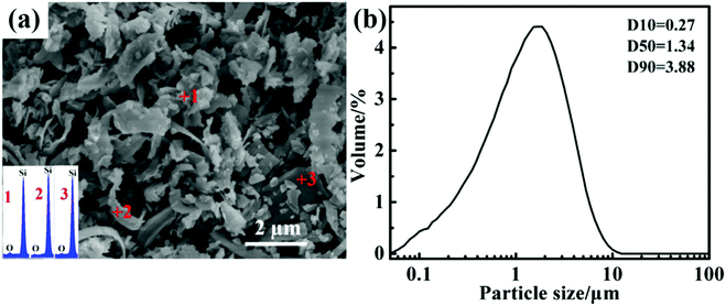 |
| | Fig. 1 SEM image (a) and particle size distribution (b) of SCW. | |
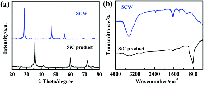 |
| | Fig. 2 XRD (a) and FTIR (b) spectra of SCW and SiC product. | |
Table 1 Chemical analysis of the SCW
| Component |
Silicon |
Silicon oxide |
Diamond |
Metallic purities |
| Contents/(wt%) |
79.80 |
15.14 |
2.10 |
2.70 |
Fig. 2 displays the XRD (a) and FTIR (b) patterns of SCW and synthesized SiC nanoparticles. As can be seen from the XRD pattern of SCW, all the diffraction peaks could be indexed to the Si and no other crystalline impurities were detected. Five reflection peaks of the synthesized SiC at 2θ = 35.6, 41.4, 60.0, 71.8 and 75.5° correspond to (111), (200), (220), (311) and (222) phases of 3C–SiC (JCPDS no. 29-1129), respectively. It is worth noting that a small diffraction peak appear at 33.6° (denoted as SF), which is resulted from the stacking fault on the [111] phase in the cubic silicon carbide.27 The FTIR spectra of SCW and synthesized SiC both showed absorption bands at 3400 and 1630 cm−1 due to the O–H stretching and bending vibrations of physically absorbed H2O and surface –OH groups.28 Two major peaks are registered at around 605 and 1065 cm−1 in the FTIR spectrum of SCW, which is attributed to Si–O and Si–O–Si stretching vibrations.15 It can be interpreted that SCW is inevitably oxidized during slicing process. In the synthesized SiC infrared spectrum, there is only one significant Si–C vibration that can be noticed at 819 cm−1.29 It was noted that no other impurities are found from the FTIR patterns of the synthesized SiC, which is consistent with XRD results suggesting a complete reaction of SCW with sucrose.
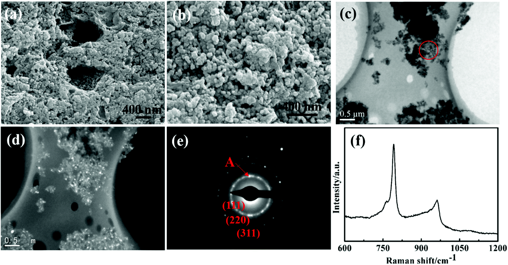
As shown in Fig. 3, the morphologies and structures of the generated SiC nanoparticles was investigated by SEM, TEM, SAED and Raman analysis. Fig. 3(a) and (b) are the SEM images of the SiC, which shows the formation of the ordered and sphere-like nanoparticles in shape. As well as the nanoparticle are slightly agglomerated it is because of long reaction time. Fig. 3(c) and (d) are the TEM images of the bright field and (111) oriented dark field of the selected area of the sample. It can be seen that the obtained SiC is composed of nanoparticles with a narrow diameter distribution of 40–50 nm. It is basically consistent with the result calculated by Scherrer formula at 40 nm. Fig. 3(e) shows a typical selected area diffraction of the SiC nanoparticles, which display a polycrystalline phase and each diffraction ring can be well indexed to the (111), (220), (311) planes of the cubic SiC, respectively. Fig. 3(f) shows the Raman spectrum of the synthesized SiC nanoparticles, it can be clearly seen that two main peaks exist at 791 and 961 cm−1, which is attributed to the characteristic transverse mode (TO) and longitudinal mode (LO) of 3C–SiC. Compared with the bulk SiC, a shift of 4–8 cm−1 toward low energy may be attributed to the quantum confinement effect and stacking faults of the SiC nanoparticles.30 The result is consistent with XRD result. At the same time, the sharp peaks confirm that the synthesized SiC nanoparticles are fine and well crystalized. These above results demonstrate that SCW can be used as secondary sources to synthesize valuable nano-SiC. The possible mechanism of the synthesis of nano-SiC can be inferred as follows: the nano-SiC is suggested to be generated through heterogeneous reaction and gas phase reaction. When the temperature was above 200 °C, sucrose is dehydrated and concentrated. With further increase of the temperature, the sucrose is carbonized and CO gas is produced. Carbon radicals with high energy is generated at about 450 °C, which intend to react with another carbon radical and form C–C linkage because of their high catenation properties.31 The newly formed carbon radicals, CO and C–C can be used as active carbon reductants. In our experimental, substituting Si powders with the SCW but containing SiO2 on the surface of the Si particle. Firstly, SiO2 film on the surface of Si is gradually consumed by reacting with carbon reductants to formation of the SiC nucleus at a relatively low temperature (eqn (1) and (2)), it is because that the SiO2 film is amorphous and high activity. Subsequently, as the SiO2 film was consumed, the inner Si is exposed and reacted by CO and carbon radicals to form SiO and SiC (eqn (3) and (4)). Then, the growth of SiC nanoparticles is regarded as the deposition reaction of SiO and CO on the SiC nucleus (eqn (5)). The growth mechanism of SiC nanoparticles is agreement with the previous reports.32,33 In addition, with the temperature rose to 1414 °C (Si mp), Si particles melt and which facilitated the formation of the SiC nanoparticles. The flow of argon gas can protect the SiC nanoparticles from being oxidized during the whole reaction process. The synthesis of SiC nanoparticle by SCW can be explained by the following equations:
| | |
SiO2(s) + 3C(s) → SiC(s) + 2CO(g)
| (1) |
| | |
SiO2(s) + 3CO(s) → SiC(s) + 2CO2(g)
| (2) |
| | |
Si(s, l) + C(s) → SiC(s)
| (3) |
| | |
Si(s, l) + CO(s) → SiC(s) + SiO(g)
| (4) |
| | |
SiO(g) + CO(g) → SiC(s) + SiO2(s)
| (5) |
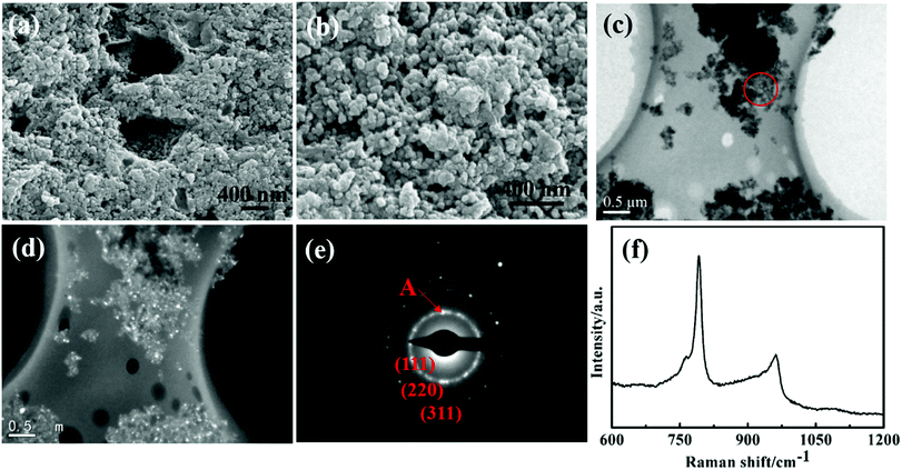 |
| | Fig. 3 (a and b) SEM images SiC product, (c and d) TEM images of SiC product in the light and dark filed, (e) the corresponding selected area electron diffraction (SAED) and (f) Raman spectrum of SiC product. | |
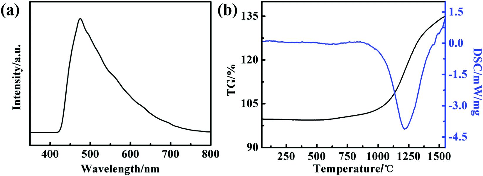
The room-temperature photoluminescence (PL) spectrum (with the excitation wavelength of 230 nm) of the obtained SiC products is shown in Fig. 4(a). A peak with strong intensity can be clearly observed at 475 nm, the emission peak for the obtained SiC product is obviously blue-shifted, compared with the previously reported PL of nanometer-sized SiC.34,35 Feng et al.36 regarded that the blue-shift of the PL maybe attribute to quantum size effects of the nanoparticles. Other reports also consider that the morphology, defects and quantum size of the SiC nanoparticle might lead to the blue-shift of the PL peak.37–39 Combined with the defects of nano-SiC in XRD results, the blue-shift of the PL peak in our study may be attributed to the defective morphology of the SiC and quantum size effects of nanomaterials. However, its exact luminescence mechanism and the exact reasons needs further study. The TGA-DTA analysis (under a flow of air in the temperature range from 25 to 1550 °C) of the obtained SiC product is shown in Fig. 4(b). It can be noticed that the weight of SiC is almost unchanged and the exothermic and endothermic peak is not present blow 700 °C, which indicates that SiC product has good thermal stability. In the range of 700–1000 °C, a slight increase of the SiC weight can be ascribed to the oxidation of SiC surface, which generates a thin film of SiO2 and slow the oxidation rate of SiC. As the temperature increases to about 1200 °C, a significant exothermic peak and an increasing of the weight of SiC appear. This phenomenon can be ascribed to the crystal transition of SiO2, which results in the cracking of film layer. Subsequently, the SiC product is further oxidized under the oxidative atmosphere. These phenomena are consistent with other reports.40,41
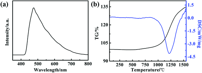 |
| | Fig. 4 PL spectrum (a) and TGA analysis (b) of the synthesized SiC. | |
4. Conclusion
Silicon cutting waste and sucrose were used as raw materials to produce SiC nanoparticles by a carbothermal reduction process in this paper. SiC nanoparticles with a size of 40–50 nm and in the shape of a sphere were successfully prepared. The synthesized SiC nanoparticles possess special photoluminescence and good thermal stability. Hence the SiC nanoparticles are expected to be applied in many potential applications such as in ultraviolet light-emitting diodes and functional ceramics materials. The possible formation mechanism of the SiC is suggested to be the heterogeneous reaction and gas phase reaction. This innovative approach can be an effective solution to reduce silicon cutting waste and decrease the cost of synthesizing SiC nanoparticles simultaneously.
Conflicts of interest
There are no conflicts to declare.
Acknowledgements
This work was financially supported by the National Key Research and Development Program of China (Grant No. 2017YFB0310302, 2018YFC1901804, and 2018YFC1901805).
References
- K. Hachichi, A. Lami, H. Zemmouri, P. Cuellar, R. Soni, H. Ait-Amar and N. Drouiche, Silicon, 2018, 3, 1–11 Search PubMed
 .
. - H. Wu, Precis. Eng., 2016, 43, 1–9 CrossRef CAS .
- C. F. Yang, H. P. Hsu and C. W. Lan, Sep. Purif. Technol., 2015, 149, 38–46 CrossRef CAS .
- Y. Zhang, Y. Hu, H. Zeng, L. Zhong, K. Liu, H. Cao, W. Li and H. Yan, J. Hazard. Mater., 2017, 329, 22–29 CrossRef CAS PubMed .
- Y.-C. Lin and C. Y. Tai, Sep. Purif. Technol., 2010, 74, 170–177 CrossRef CAS .
- S. Liu, K. Huang and H. Zhu, Sep. Purif. Technol., 2013, 118, 448–454 CrossRef CAS .
- L. Tong, T. Yi, L. Jiayan and D. Dewei, J. Cleaner Prod., 2018, 203, 574–584 CrossRef .
- K. Tomono, H. Furuya, S. Miyamoto, Y. Okamura, M. Sumimoto, Y. Sakata, R. Komatsu and M. Nakayama, Sep. Purif. Technol., 2013, 103, 109–113 CrossRef CAS .
- L. Huang, J. Chen, F. Ming, S. Thomas, A. Danaei, X. Luo and M. Barati, J. Cleaner Prod., 2018, 186, 718–725 CrossRef CAS .
- J. Li, P. Ni, L. Wang and Y. Tan, Mater. Sci. Semicond. Process., 2017, 61, 79–84 CrossRef CAS .
- J. Kong, P. Xing, Y. Liu, J. Wang, X. Jin, Z. Feng and X. Luo, Silicon, 2019, 11, 367–376 CrossRef CAS .
- Y. Luo, S. Zheng, S. Ma, C. Liu, J. Ding and X. Wang, Ceram. Int., 2018, 44, 10585–10595 CrossRef CAS .
- S. Adhikari, N. K. Eswar, S. Sangita, D. Sarkar and G. Madras, J. Photochem. Photobiol., A, 2018, 357, 118–131 CrossRef CAS .
- J. Ding, C. Deng, W. Yuan, H. Zhu and X. Zhang, Ceram. Int., 2014, 40, 4001–4007 CrossRef CAS .
- R. Rajarao, R. Ferreira, S. H. F. Sadi, R. Khanna and V. Sahajwalla, Mater. Lett., 2014, 120, 65–68 CrossRef CAS .
- T. Serdiuk, S. A. Alekseev, V. Lysenko, V. A. Skryshevsky and A. Geloen, Nanotechnology, 2012, 23, 315101 CrossRef CAS PubMed .
- Z. G. Sun, X. J. Qiao, Q. G. Ren, X. D. Guo, L. Wei, P. Z. Liu and W. C. Li, Adv. Powder Technol., 2016, 27, 1552–1559 CrossRef CAS .
- C. C. Chen, H. P. Tseng, T. Y. Huang, J. C. Kuo and G. L. Huang, Mater. Chem. Phys., 2009, 116, 497–502 CrossRef CAS .
- T. Seeger, P. Kohler-Redlich and M. Rühle, ChemInform, 2000, 4, 279–282 Search PubMed .
- J. X. Chang, R. Z. Liu, M. L. Liu, Y. L. Shao and B. Liu, Key Eng. Mater., 2016, 697, 841–845 Search PubMed .
- A. Najafi, F. G. Fard, H. R. Rezaie and N. Ehsani, Powder Technol., 2012, 219, 202–210 CrossRef CAS .
- M. D. Clark, L. S. Walker, V. G. Hadjiev, V. Khabashesku, E. L. Corral, R. Krishnamoorti and M. Cinibulk, J. Am. Ceram. Soc., 2011, 94, 4444–4452 CrossRef CAS .
- M. Lu, A. Li, T. Wang, D. Wang and W. Qin, J. Nanosci. Nanotechnol., 2010, 10, 2135–2138 CrossRef CAS PubMed .
- R. R. Rajagopal, R. Rajarao and V. Sahajwalla, Compos. Commun., 2017, 5, 19–22 CrossRef .
- Z. Ju, X. Ma, N. Fan, P. Li, L. Xu and Y. Qian, Mater. Lett., 2007, 61, 3913–3915 CrossRef CAS .
- S. Maroufi, M. Mayyas and V. Sahajwalla, ACS Sustainable Chem. Eng., 2017, 5, 4171–4178 CrossRef CAS .
- S. T. Kunihito Koumoto and C. H. Pai, J. Am. Ceram. Soc., 1989, 72, 1985–1987 CrossRef .
- S. Mingwu, C. Hongdong, W. Xifu, C. Xueyan, L. Kangan, W. Su He, G. Rui, Z. Linfeng, Z. Guixiang and S. Xiangyang, Nanotechnology, 2012, 23, 40 Search PubMed .
- R. Rajarao and V. Sahajwalla, J. Cleaner Prod., 2016, 133, 1277–1282 CrossRef CAS .
- L. Wang, Q. Cheng, H. Qin, Z. Li, Z. Lou, J. Lu, J. Zhang and Q. Zhou, Dalton Trans., 2017, 46, 2756–2759 RSC .
- R. Atchudan, S. Perumal, T. N. Jebakumar Immanuel Edison and Y. R. Lee, Mater. Lett., 2016, 166, 145–149 CrossRef CAS .
- S. Cetinkaya and S. Eroglu, Int. J. Refract. Met. Hard Mater., 2011, 29, 566–572 CrossRef CAS .
- J. Chen, L. Ding, L. Xin, F. Zeng and J. Chen, J. Solid State Chem., 2017, 253, 282–286 CrossRef CAS .
- H. W. Shim, K. C. Kim, Y. H. Seo, K. S. Nahm, E. K. Suh, H. J. Lee and Y. G. Hwang, Appl. Phys. Lett., 1997, 70, 1757–1759 CrossRef CAS .
- Y. Zhang, M. Nishitani-Gamo, C. Xiao and T. Ando, J. Appl. Phys., 2002, 91, 6066–6070 CrossRef CAS .
- D. H. Feng, Z. Z. Xu, T. Q. Jia, X. X. Li and S. Q. Gong, Phys. Rev. B: Condens. Matter Mater. Phys., 2003, 68, 204–213 CrossRef .
- J. Chen, R. Wu, G. Yang, Y. Pan, J. Lin, L. Wu and R. Zhai, J. Alloys Compd., 2008, 456, 320–323 CrossRef CAS .
- N. Jun Jie and W. Jian Nong, J. Phys. Chem. B, 2007, 111, 4368–4373 CrossRef PubMed .
- Z. Ju, Z. Xing, C. Guo, L. Yang, L. Xu and Y. Qian, Eur. J. Inorg. Chem., 2008, 2008, 3883–3888 CrossRef .
- S.-W. Park, J.-C. Kim, B.-K. Kim, D.-W. Kim and B. Gao, J. Am. Ceram. Soc., 2016, 99, 1885–1888 CrossRef CAS .
- M. T. Dove, M. Gambhir and V. Heine, Phys. Chem. Miner., 1999, 26, 344–353 CrossRef CAS .
|
| This journal is © The Royal Society of Chemistry 2019 |
Click here to see how this site uses Cookies. View our privacy policy here. 
 Open Access Article
 This Open Access Article is licensed under a Creative Commons Attribution-Non Commercial 3.0 Unported Licence
 a,
Shuaibo Gaoa,
Jian Konga,
Xing Jinb,
Donghui Weia,
Dagang Lia and
Pengfei Xing
a,
Shuaibo Gaoa,
Jian Konga,
Xing Jinb,
Donghui Weia,
Dagang Lia and
Pengfei Xing