
 Open Access Article
 This Open Access Article is licensed under a Creative Commons Attribution-Non Commercial 3.0 Unported Licence
Self-formed silver nanoparticles on freestanding silicon nanowire arrays featuring SERS performances†
Pin-Ju Chiena,
Yongcun Zhoub,
Kun-Hung Tsaia,
Hong Phan Duong c and
Chia-Yun Chen*ad
c and
Chia-Yun Chen*ad
aDepartment of Materials Science and Engineering, National Cheng Kung University, No. 1 University Road, Tainan 70101, Taiwan. E-mail: timcychen@mail.ncku.edu.tw
bSchool of Materials Science and Engineering, Northwestern Polytechnical University, Xi'an 710072, Shaanxi, People's Republic of China
cThe University of Danang, University of Science and Technology, 54 Nguyen Luong Bang, Vietnam
dHierarchical Green-Energy Materials (Hi-GEM) Research Center, National Cheng Kung University, No. 1 University Road, Tainan 70101, Taiwan
First published on 20th August 2019
Abstract
Herein, the universal luminescence characteristics of porous Si nanowire arrays were exploited using a wide range of doping types and concentrations; we found that the dual-band photoluminescence intensities were correlated with the formation rates of Si nanowires with porous features; however, these intensities exhibited no evident dependence on the doping conditions. Furthermore, we demonstrated a facile and reliable transfer method implementing the freestanding Si nanowire arrays while maintaining the robust photoluminescence behaviors under bending conditions. The fabrication protocol, involving lateral etching locally at the nanowire ends, enabled the controlled formation of uniform and large-area transferred nanowires with vertical regularity. Without the additional deposition of Ag nanoparticles, these transferred Si nanowire films inherently possessed SERS sensing capability with a relative enhancement factor over 1.8 times that of the Si nanowires with electroless-deposited Ag nanoparticles, which could practically emerge as a functional design for the integration of practical biochip devices.
Introduction
In the past several decades, the optical properties of low-dimensional silicon (Si) structures have attracted worldwide interest for the development of next-generation Si optoelectronics. This was particularly stimulated by the observation of room-temperature photoluminescence (PL) of Si with porous features.1,2 Although many potential fabrication techniques have been reported for the preparation of vertically aligned porous Si nanowire (SiNW) arrays with visible-light emission,3–6 the detachment of porous SiNWs from bulk Si substrates while maintaining their vertical architectures remains highly challenging; this can limit the potential applications of these arrays due to the inherent optical and optoelectronic properties of Si nanostructures rather than the overwhelming contributions from the bulk Si substrates. Moreover, it is practically desirable to transfer the vertically arranged SiNWs to a foreign substrate for the realization of functional devices with high flexibility;7–10 one compelling example is the design of high-performance SERS, which has been considered as an ultrasensitive strategy for the extraction of molecular information from complex biological environments and can even enable the detection capability of up to the single-molecule level.11On the basis of strong localized surface plasmon resonance (LSPR) excitation, the electromagnetic field near the surfaces of noble metal nanoparticles is significantly enhanced, offering more intense Raman scattering from the detected molecules. However, the sensing performance highly relies on the spatial position of metal nanoparticles, where the particle size, shape and arrangement should be maintained for providing a reproducible and reliable SERS effect.12 In this regard, the freestanding SiNW arrays could act as promising host materials, which enabled the stabilization of dispersed metal nanoparticles on SiNW sidewalls against aggregation that could significantly degrade their sensing performance. Essentially, an additional deposition process, such as electroless plating,13 drop coating,14 physical deposition and hydrothermal growth,15–17 for coating metal nanoparticles on SiNWs is required, which may be time consuming and challenging to create spatially distributed features that are necessary to provide high SERS sensitivity. Overall, in this study, we demonstrated flexible SERS sensors by implementing the controlled formation of freestanding porous SiNWs decorated with self-formed Ag nanoparticles (AgNPs). To achieve this aim, we exploited a transfer technique involving lateral etching locally at the end of the SiNW arrays. Bending tests to determine the light-emitting characteristics of transferred SiNW structures were conducted to examine the reliability of the transfer process. We further found that these freestanding SiNW films possessed a remarkable SERS sensing performance owing to the inherent decoration of the dispersed AgNPs on SiNWs.
Experimental details
Fabrication
Single-crystalline and (100)-oriented Si substrates made by the Czochralski method with various dopant types and concentrations, including n+ (0.1–0.5 ohm cm), n (1–10 ohm cm), p (1–10 ohm cm), p+ (0.1–0.5 ohm cm) and p++ (0.01–0.05 ohm cm), were utilized for the preparation of solid and porous SiNW arrays. Prior to the etching reaction, the Si substrates were carefully cleaned several times via ultrasonication with acetone, isopropyl alcohol (IPA) and deionized water (DI). After this, two distinct metal-assisted chemical etching (MaCE) processes were performed for the preparation of regular Si nanowire arrays.18–22 In the one-step MaCE method, the Si substrates were immersed in the etching solutions containing 0.02 M of AgNO3 and 4.6 M of HF at 30 °C for 10 min. In the two-step MaCE method, the Si substrates were dipped in the mixed solution containing 0.005 M of AgNO3 and 4.6 M of HF at 25 °C for 10 s and subsequently transferred to another etching solution containing 0.3 M of H2O2 and 4.6 M of HF at 30 °C for 10 min. After performing the etching experiments, the nanowire-based samples were rinsed with DI water and dried under a gentle flow of N2 gas. The electroless deposition of Ag nanoparticles on either SiNWs or bare Si substrates was conducted by immersing the samples in an electrolyte solution containing 0.005 M of AgNO3 and 4.8 M of HF at room temperature for 25 s and then rinsing with DI water followed by drying under a stream of N2 gas.Characterizations
The microstructures and morphologies of the Si nanowires were characterized using a transmission electron microscope (TEM, JEOL 2100) and a scanning electron microscope (SEM, LEO 1530), respectively. The chemical compositions of the as-formed Ag nanoparticles were analyzed using an energy dispersive spectrometer (EDS, Oxford INCA). PL investigations were performed at room temperature using a light source of a light-emitting diode lamp (the outpower of 780 mV) with the center wavelength of 365 nm. Raman measurements were performed using a Raman spectrometer (Jobin Yvon) based on the laser wavelength of 532 nm.Results and discussion
Herein, two types of SiNWs were prepared via distinct etching techniques: one-step MaCE and two-step MaCE process, as detailed in the experimental section. The involved reaction of the one-step MaCE process could be represented as follows:23| Si + 6HF + 4Ag+ → H2SiF6 + 4H+ + 4Ag | (1) |
The overall etching was initiated by the reduction of Ag+ ions supplied from AgNO3 precursors that created the Ag seeds on Si surfaces, which could be attributed to the fact that the reduction potential of Ag+/Ag was more positive than the Fermi level of Si. Moreover, these formed Ag seeds oxidized the underlying Si atoms through hole injections. The etching reaction was sustained along the 〈100〉 orientations by cycling reactions that included the removal of oxidized Si and reduction of the Ag+ ions from the aqueous solution, eventually leaving the vertically aligned solid SiNWs behind, as illustrated in the inset image of Fig. 1(a). The corresponding TEM image is presented in Fig. 1(b), indicating that the nanowire sidewalls remain crystalline and maintain the consistent atomic configuration with inner regions.
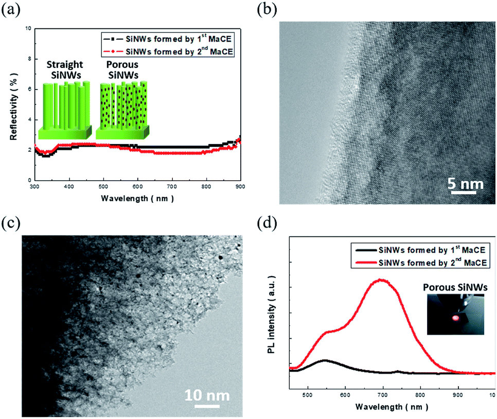 | ||
| Fig. 1 (a) Light absorption spectra of both solid and porous SiNW arrays. Representative TEM images of a (b) solid SiNW and (c) porous SiNW. (d) Photoluminescence spectra of both solid and porous SiNW arrays. The inset figure shows the image of porous SiNWs illuminated with a 365 nm light. | ||
In addition, by employing the two-step MaCE process, straight SiNWs were created through the following electrochemical reaction:24,25
| Si + n/2H2O2 + 6HF → nH2O + H2SiF6 + (4 − n)/2H2 | (2) |
The etching of Si preferentially occurred along the 〈100〉 direction, where the straight sinking of the predefined Ag seeds into the Si substrates was accomplished with the local oxidation and dissolution of Si in contact with the Ag seeds; although the vertical movement of the Ag seeds relative to the substrate planes dominated the etching reaction, the local dissolution of Ag seeds also occurred due to the lower electrochemical potential of Ag with respect to that of the involved H2O2 oxidants. This increased the number of Ag+ ions that preferentially re-nucleated on the rough sidewalls of the etching pores owing to the lower energy barrier required at these defective sites. With the continuous supply of H2O2 molecules, it could be expected that the localized etching was initiated by these newly formed Ag nuclei in conjunction with the continuous sinking of primary Ag seeds. This accounted for the formation of porous features in these one-dimensional Si nanostructures, as depicted in the inset of Fig. 1(a). These findings could be further supported by the TEM investigations, and the highly porous features on the nanowire sidewalls could be clearly observed, as evidenced in Fig. 1(c).
The corresponding light-absorption spectra of both solid and porous SiNWs are presented in Fig. 1(a), and no distinguishable features are present in the spectra of these two samples. Specifically, the average reflectivity was found to be 1.95% (solid SiNWs) and 1.86% (porous SiNWs). This indicated that the effect of light trapping dominated the optical absorptivity of SiNWs rather than the contributions from the nanostructure morphologies; this also implied the effective interaction of light with these two distinct SiNWs, indicating that the number of irradiated photons trapped inside these SiNWs was roughly the same. In addition, the PL spectra were compared to analyze the light-emitting properties of these SiNWs, as shown in Fig. 1(d). Contrary to the similar light-absorption behaviours, the PL characteristics of SiNWs were found to be highly correlated with the microstructures of the tested SiNWs. The remarkable and dual PL patterns centred at both 546 and 695 nm could be obtained from the porous SiNWs made using the two-step MaCE process, whereas the comparatively weaker PL peak centred at 546 nm was found from the solid SiNWs prepared using the one-step MaCE method. Since both nanostructures could efficiently absorb the incoming light, the subsequent radiative recombination of excited charges was therefore determined by the surface structures of the light-excited SiNWs. The highly porous features appearing in the large-area skeletons of the nanowire structures could facilitate charge recombination radiatively for generating the strong red lights (center wavelength = 695 nm) that could even be observed by the naked eye, as shown in the inset of Fig. 1(d). Moreover, the wideband blue/green-light emissions (center wavelength = 546 nm) have been reported to originate from the rough surfaces of SiNWs,26,27 which could be observed from both the porous and solid SiNW architectures.
To exploit the universal luminescence characteristics of porous SiNWs excited by light, the two-step MaCE process was conducted under a wide range of doping conditions for Si substrates for the preparation of porous SiNWs with various doping levels. The comparative PL spectra reflected that the dual emission peaks of various doped SiNWs were present regardless of the doping types and concentrations, revealing that the similar light-emission mechanism was dominantly contributed by the porous nature of the formed SiNWs under a wide range of doping conditions, as presented in Fig. 2(a). Since the size and distribution of the created pores in the nanowire sidewalls were unlikely to be identical for different doped SiNWs, the effects of quantum confinement on the size-dependent emission characteristics were less validated. Instead, the PL intensities of the predominant red-light emission were dramatically different, where the porous SiNWs with slight p-doping (denoted as p SiNWs) presented the highest emission intensity, which was above 3.9 times higher than that of the heavily p-doped SiNWs (denoted as p++ SiNWs).
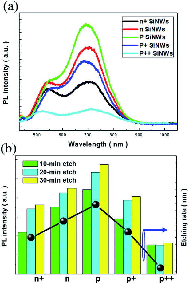 | ||
| Fig. 2 (a) Photoluminescence spectra of porous SiNW arrays under various doping conditions, including n+ (moderately n-doped), n (lightly n-doped), p (lightly p-doped), p+ (moderately p-doped) and p++ (heavily p-doped) types. (b) Comparative PL intensity at 695 nm of various doped SiNW arrays under three different etching durations. The corresponding etching rates for the formation of SiNW arrays were also compared. | ||
We attributed the substantial change of emission capability to the numbers of involved pores in the Si nanocrystallites that provided effective sites for light emission. In this regard, a change in the PL intensity seemed to be correlated with the formation rate of porous SiNWs. To examine this hypothesis, a systematic validation of the doped SiNWs fabricated with various etching durations was performed, as shown in Fig. 2(b). Similar PL characteristics were presented regardless of the doping conditions and etching durations, and the universal trends in terms of PL intensity were observed: highest PL intensity was obtained from the slightly p-doped SiNWs, followed by the slightly n-doped SiNWs (n SiNWs), moderately p-doped SiNWs (p+ SiNWs), moderately n-doped SiNWs (n+ SiNWs) and heavily p-doped SiNWs. On the other hand, from the investigations of the etching rates of various doped Si substrates, it could be found that in a similar doping concentration range, the p-doped SiNWs possessed slightly higher etching rate than the n-doped SiNWs owing to the fact that the excess holes existing in the Si crystals facilitated the oxidation reaction in the presence of H2O2/HF solutions.28 However, although the doping concentrations in the p type material reached moderately or even heavily doped levels, the accumulation of excessive holes at the Ag/Si interfaces created a biased potential that decelerated the succeeding Si oxidation from the hole injections of H2O2 oxidants, thus slowing down the etching rates. Accordingly, we found that the universal dependence of PL intensity explicitly corresponded to the etching rate for the formation of porous SiNWs, as evidenced in Fig. 2(b). Moreover, this further verified that the PL intensity of various doped porous SiNWs made using this simple, reliable and room-temperature-processing method could be essentially tuned by controlling the etching durations, which might pave a rational way for synthesizing light-emitting Si nanostructures under controlled doping conditions.
In addition to the study on the PL properties of porous SiNWs, we further attempted to vertically transfer the regular porous SiNWs onto flexible receiver substrates. This could benefit the realization of Si-based vertical devices with flexible functionality. Fig. 3 illustrates the process flow for the detachment of functional SiNWs, followed by their complete transfer to the adhesive substrates through the facile and reliable lateral etching process. After conducting the two-step MaCE process for the preparation of porous SiNWs with desired lengths, the samples were rinsed with DI water for the complete removal of residual etchants. To initiate the lateral breakage at the end of the SiNWs, two consecutive steps were conducted for the dissolution of the Ag seeds: the re-nucleation of Ag nanoparticles followed by catalytic etching along the lateral directions. These were accomplished by immersing the as-prepared SiNWs in H2O2 solutions (0.3 M) for 1 min and subsequently transferring them to the etching solutions containing HF (4.8 M) and H2O2 (1 M) solutions for 1.5 min at room temperature. This would create cracks at the SiNW ends and underlying substrates, thus facilitating the detachment of freestanding SiNWs from the substrates.
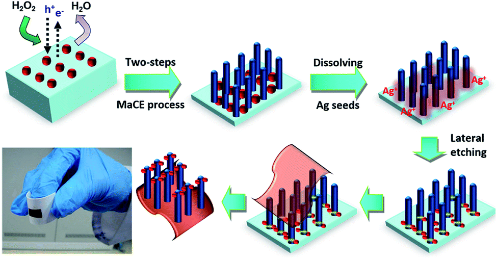 | ||
| Fig. 3 Schematic process flow for the preparation of freestanding SiNW films with vertical regularity through the introduction of lateral etching locally at nanowire ends and followed by transfer to the receiver substrate. The representative image of the transferred SiNWs is also presented. | ||
It has been reported that the Ag seeds intend to be dissolved in H2O2 solutions due to the reduction potential difference;29,30 this results in the formation of abundant Ag+ ions attached in the bottom regions of the SiNWs. When the H2O2/HF etchants were introduced, these concentrated Ag+ ions were reduced by hole injections from the H2O2 oxidants and then favourably nucleated as new Ag nanoparticles in the proximity of SiNW ends due to the shortest diffusion distance. These newly formed Ag nanoparticles acted as catalysts that facilitated the lateral etching vertically towards the sidewalls of the SiNWs, thus weakening the bonding of the SiNW films with the underlying substrates. This created the end-fractured SiNW films while maintaining the structural integrity of the vertical features that could be facilely separated from the mother substrates by peeling off the attached substrates, thus successfully being transferred onto the receivers in a larger area, as shown in Fig. 3.
The detailed morphologies of the SiNWs before and after the transfer process are shown in Fig. 4, and the robust connection between the aligned porous SiNWs and Si substrates as starting materials can be observed in Fig. 4(a). By adapting the lateral etching for the creation of sidewall breakage at the SiNW ends, it horizontally broke the connection with the underlying bulk part, and thus, the freestanding SiNW films were formed, as presented in Fig. 4(b). Fig. 4(c) further demonstrates the top-view comparative image showing that only the etched pits are left on the substrate surfaces after the transfer process, which indicates the uniform and large-area processing capability with no local defects or discontinuity arising from the transfer method. The cross-sectional SEM images of the transferred SiNWs films attached on the adhesive substrates are presented in Fig. 4(d), where the well-preserved alignment of the vertical configuration can be observed. To obtain an insight into the PL characteristics of the transferred SiNW films, a series of PL measurements under various bending angles were conducted, as shown in Fig. 5. The PL spectrum of flexible SiNWs was obtained for each case, i.e. a flat case, curved angles of 10°, 20° and 40°, and then recovery to the original flat condition. Obviously, the measured PL spectra under the abovementioned tested conditions were explicitly overlapped, highlighting the robustness and reliability of the created SiNW films.
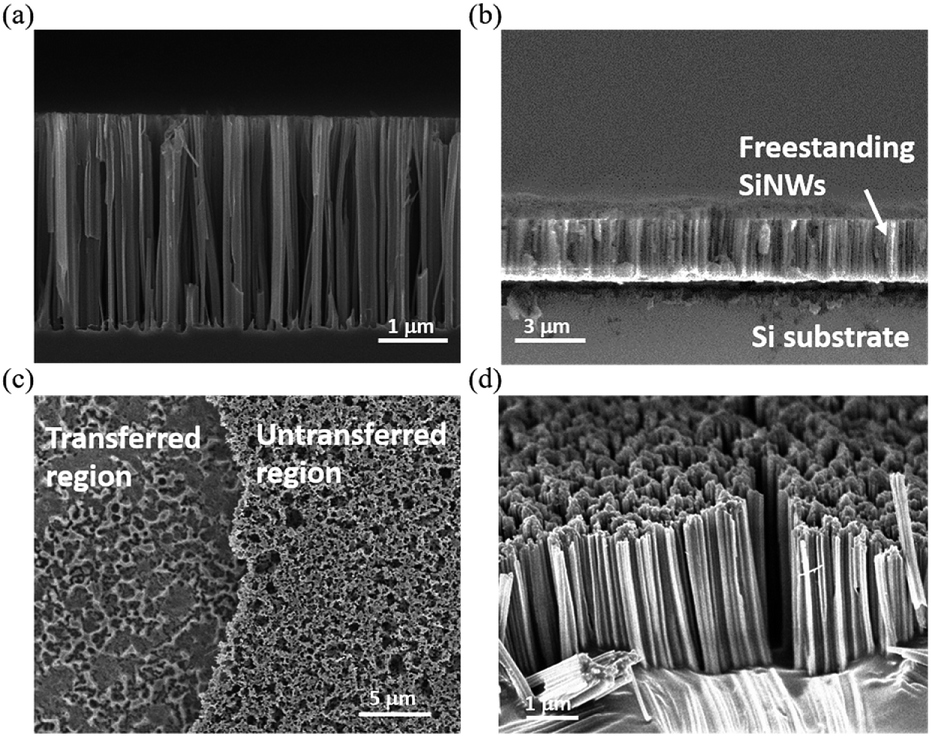 | ||
| Fig. 4 Cross-sectional SEM images of the SiNW arrays (a) before and (b) after introducing the lateral etching at the SiNW ends. (c) Top-view SEM image of the mother substrate. (d) Cross-sectional SEM image of the transferred SiNW arrays. | ||
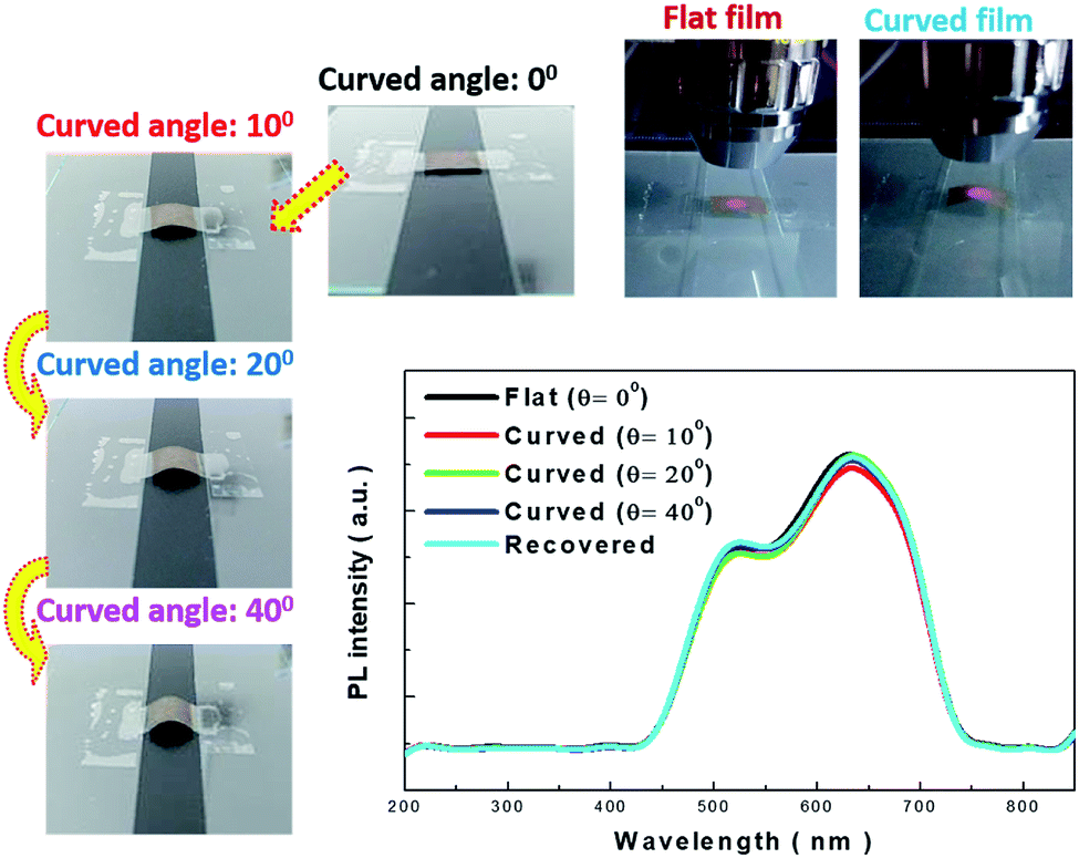 | ||
| Fig. 5 Photoluminescence examinations of freestanding SiNW films under various bending angles. Each image presents the bending condition of the SiNW films for testing. | ||
Finally, the capability of SERS sensing based on the transferred SiNWs was exploited. Unlike the reported SERS sensors where the deposition of noble metals serving as hot spots for enhancing the Raman signals was required,31–33 these transferred SiNWs inherently constituted the hybrid architecture of AgNPs with the sizes of 5–14 nm and porous SiNW supporters. These self-formed features were attributed to the employed lateral etching of SiNWs that rendered the simultaneous formation of freestanding SiNW arrays and incorporated AgNPs. These were identified by the TEM investigation along with the EDS analysis of a representative freestanding SiNW, as shown in Fig. 6(a) and the ESI.† The SERS sensing performances were evaluated by placing the R6G dye (10−7 M) as a detection target on various sample surfaces, including the freestanding SiNW films with self-formed AgNPs, SiNWs/Si substrates and Si substrates decorated with electroless-deposited AgNPs, and bare Si substrates. In addition, the measurements were conducted on the samples without bending. The corresponding Raman spectra are presented in Fig. 6(b), showing the marked Raman peaks at 1311, 1511 and 1575 cm−1. This indicated that the incorporation of AgNPs into SiNWs enhanced the SERS signals than the case of the Si substrates with directly deposited AgNPs; these results could be attributed to the large surface area of SiNWs that enabled the loading of more AgNPs as active spots for the strengthening of the Raman features through the field localization of the incoming light. By contrast, the bare Si substrates presented inactive Raman interactions in the detection of R6G analytes at low-concentrations tested herein.
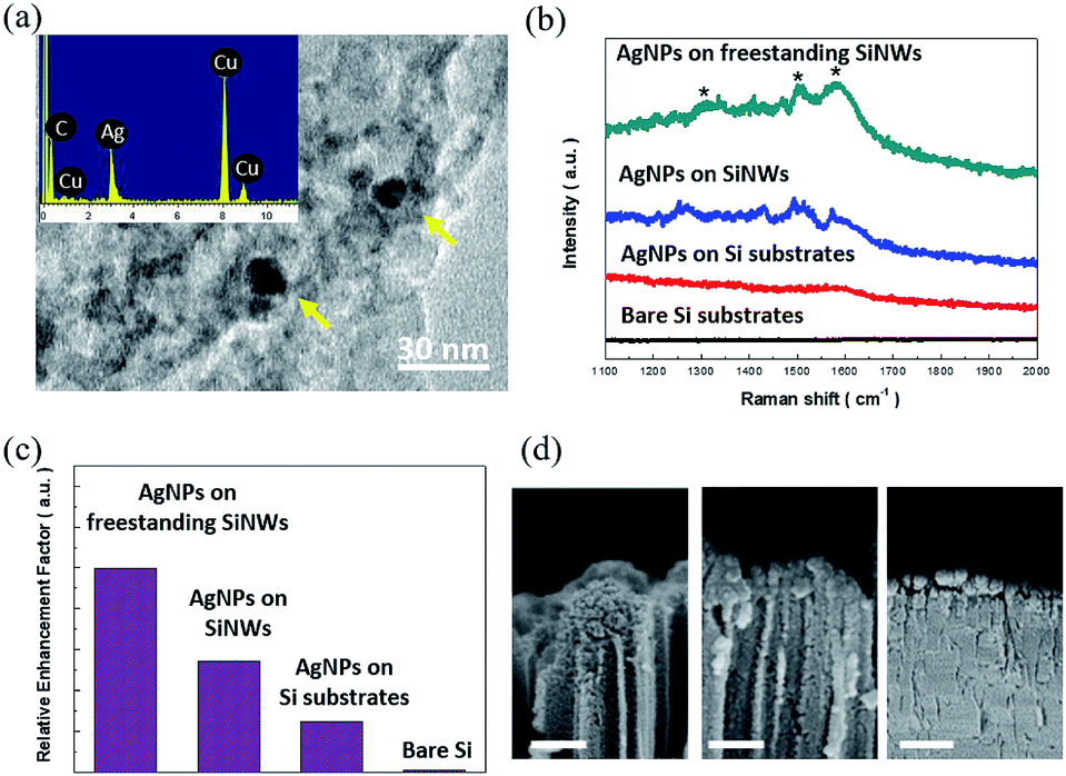 | ||
| Fig. 6 (a) Representative TEM image of a transferred SiNW. The inset figure shows the corresponding EDS analysis results, indicating that the composition of the nanoparticles denoted by a yellow arrow is Ag. The signals of the Cu and C elements originated from the TEM grid. (b) Comparative Raman spectra of various SERS substrates. (c) Examination of the relative enhancement factor of various samples extracted from Raman spectra. (d) Cross-sectional SEM images of the sample surfaces including freestanding AgNPs/SiNWs (left figure), AgNPs/SiNWs on the Si substrates (middle figure) and AgNP-loaded Si substrates (right figure). The scale bar is 200 nm. | ||
To further compare their sensing capabilities, the relative enhancement factors (REFs) of Raman sensing were evaluated:34,35
| REFs = Isubstrate,A × Nsubstrate,A/Isubstrate,B × Nsubstrate,B | (3) |
Conclusions
In conclusion, systematic investigations on the PL characteristics of porous SiNW arrays were performed by varying the wide range of doping conditions. The resulting PL intensity was found to be highly dependent on the formation rates of porous features regardless of the doping types and concentrations. In addition, these porous Si nanowires with sound flexibility could be successfully detached from the original mother substrates using a facile and reliable transfer method while maintaining the robust PL properties under the bending conditions. Moreover, unlike the reported SERS sensors where the additional preparation of metal nanoparticles as hot spots for enhancing Raman signals was required, these transferred SiNWs inherently rendered the simultaneous formation of freestanding SiNW arrays and decorated AgNPs, thus resulting in remarkable SERS sensing performances with improved REFs over 1.8 times higher than those of the SiNWs with electroless-deposited AgNPs. This design could open new routes to the self-formed and flexible SERS sensing platform, with a potential impact on biological detection, chemical analysis and other functional applications.Conflicts of interest
There are no conflicts of interest to declare.Acknowledgements
This study was financially supported by the Ministry of Science and Technology of Taiwan (MOST 107-2221-E-006-013-MY3), and Hierarchical Green-Energy Materials (Hi-GEM) Research Center, from the Featured Areas Research Center Program within the framework of the Higher Education Sprout Project by the Ministry of Education (MOE) and the Ministry of Science and Technology (MOST 107-3017-F-006-003) in Taiwan. The authors greatly acknowledge the Center for Micro/Nano Science and Technology, National Cheng Kung University for the facilities provided for conducting material characterizations.Notes and references
- N. Koshida and H. Koyama, Jpn. J. Appl. Phys., 1991, 30, 7B CrossRef.
- Z. Y. Xu, M. Gal and M. Gross, Appl. Phys. Lett., 1992, 60, 1375 CrossRef CAS.
- L. Lin, S. Guo, X. Sun, J. Feng and Y. Wang, Nanoscale Res. Lett., 2010, 5, 1822 CrossRef CAS PubMed.
- A. I. Hochbaum, D. Gargas, Y. J. Hwang and P. Yang, Nano Lett., 2009, 9, 3550–3554 CrossRef CAS PubMed.
- Y. Qu, H. Zhou and X. Duan, Nanoscale, 2011, 3, 4060–4068 RSC.
- Y. Qu, L. Liao, Y. Li, H. Zhang, Y. Huang and X. Duan, Nano Lett., 2009, 9, 4539–4543 CrossRef CAS PubMed.
- K. E. Plass, M. A. Filler, J. M. Spurgeon, B. M. Kayes, S. Maldonado, B. S. Brunschwig, H. A. Atwater and N. S. Lewis, Adv. Mater., 2009, 21, 325–328 CrossRef CAS.
- J. M. Spurgeon, S. W. Boettcher, M. D. Kelzenberg, B. S. Brunschwig, H. A. Atwater and N. S. Lewis, Adv. Mater., 2010, 22, 3277–3281 CrossRef CAS PubMed.
- H. Cui, S. Li, S. Deng, H. Chen and C. Wang, ACS Sens., 2017, 2, 386–393 CrossRef CAS PubMed.
- X. Chen, J. Wen, J. Zhou, Z. Zheng, D. An, H. Wang, W. Xie, R. Zhan, N. Xu, J. Chen, J. She, H. Chen and S. Deng, J. Opt., 2018, 20, 024012 CrossRef.
- K. Kneipp, Y. Wang, H. Kneipp, L. T. Perelman, I. Itzkan, R. R. Dasari and M. S. Feld, Phys. Rev. Lett., 1997, 78, 1667 CrossRef CAS.
- B. Sharma, R. R. Frontiera, A. I. Henry, E. Ringe and R. P. V. Duyne, Mater. Today, 2012, 15, 16–25 CrossRef CAS.
- F. M. Liu and M. Green, J. Mater. Chem., 2004, 14, 1526–1532 RSC.
- P. Hu, X. S. Zheng, C. Zong, M. H. Li, L. Y. Zhang, W. Li and B. Ren, J. Raman Spectrosc., 2014, 45, 565–573 CrossRef CAS.
- Y. Sun and G. P. Wiederrecht, Small, 2007, 3, 1964–1975 CrossRef CAS PubMed.
- Y. J. Liu, H. Y. Chu and Y. P. Zhao, J. Phys. Chem. C, 2010, 114, 8176–8183 CrossRef CAS.
- R. Ji, W. Sun and Y. Chu, RSC Adv., 2014, 4, 6055–6059 RSC.
- X. Li and P. W. Bohn, Appl. Phys. Lett., 2000, 77, 2572–2574 CrossRef CAS.
- J. Y. Li, C. H. Hung and C. Y. Chen, Sci. Rep., 2017, 7, 17177 CrossRef PubMed.
- Y. Chen, L. Li, C. Zhang, C. C. Tuan, X. Chen, J. Gao, Y. Ding and C. P. Wong, Nano Lett., 2017, 17, 1014–1019 CrossRef CAS PubMed.
- C. Y. Chen, T. C. Wei, P. H. Hsiao and C. H. Hung, ACS Appl. Energy Mater., 2019, 2, 4873–4881 CrossRef CAS.
- O. J. Hildreth, D. Brown and C. P. Wong, Adv. Funct. Mater., 2011, 23, 3119–3128 CrossRef.
- I. R. Putra, J. Y. Li and C. Y. Chen, Appl. Surf. Sci., 2019, 478, 725–732 CrossRef CAS.
- C. Chartier, S. Bastide and C. L. Clement, Electrochim. Acta, 2008, 53, 5509–5516 CrossRef CAS.
- Z. Huang, X. Zhang, M. Reiche, L. Liu, W. Lee, T. Shimizu, S. Senz and U. Gosele, Nano Lett., 2008, 8, 3046–3051 CrossRef CAS PubMed.
- W. Chern, K. Hsu, I. S. Chun, B. P. de Azeredo, N. Ahmed, K. H. Kim, J. min Zuo, N. Fang, P. Ferreira and X. Li, Nano Lett., 2010, 10, 1582–1588 CrossRef CAS PubMed.
- C. Y. Chen, P. H. Hsiao, T. C. Wei, T. C. Chen and C. H. Tang, Phys. Chem. Chem. Phys., 2017, 19, 11786–11792 RSC.
- Z. Huang, N. Geyer, P. Werner, J. Boor and U. Gosele, Adv. Mater., 2011, 23, 285–308 CrossRef CAS PubMed.
- X. Zhong, Y. Qu, Y. C. Lin, L. Liao and X. Duan, ACS Appl. Mater. Interfaces, 2011, 3, 261–270 CrossRef CAS PubMed.
- S. Li, W. Ma, Y. Zhou, X. Chen, Y. Xiao, M. Ma, W. Zhu and F. Wei, Nanoscale Res. Lett., 2014, 9, 196 CrossRef PubMed.
- S. L. Kleinman, R. R. Frontiera, A. I. Henry, J. A. Dieringer and R. P. V. Duyne, Phys. Chem. Chem. Phys., 2013, 15, 21–36 RSC.
- S. M. Stranahan and K. A. Willets, Nano Lett., 2010, 10, 3777–3784 CrossRef CAS PubMed.
- C. Farcau and S. Astilean, J. Phys. Chem. C, 2010, 114, 11717–11722 CrossRef CAS.
- J. M. McLellan, Z. Y. Li, A. R. Siekkinen and Y. Xia, Nano Lett., 2007, 7, 1013–1017 CrossRef CAS PubMed.
- X. Chen, C. H. Cui, Z. Guo, J. H. Liu, X. J. Huang and S. H. Yu, Small, 2011, 7, 858–863 CrossRef CAS PubMed.
- Y. Wang, H. Chen, S. Dong and E. Wang, J. Raman Spectrosc., 2007, 38, 515–521 CrossRef CAS.
Footnote |
| † Electronic supplementary information (ESI) available. See DOI: 10.1039/c9ra03273h |
| This journal is © The Royal Society of Chemistry 2019 |