
 Open Access Article
 This Open Access Article is licensed under a Creative Commons Attribution-Non Commercial 3.0 Unported Licence
Strain engineering on the electronic states of two-dimensional GaN/graphene heterostructure
Zhongxun Deng ab and
Xianhui Wang*a
ab and
Xianhui Wang*a
aShanxi Province Key Laboratory of Electrical Materials and Infiltration Technology, School of Materials Science and Engineering, Xi'an University of Technology, Xi'an 710048, Shaanxi, P. R. China. E-mail: xhwang693@xaut.edu.cn
bEnergy and Engineering College, Yulin University, Yulin 719000, Shaanxi, P. R. China
First published on 20th August 2019
Abstract
Combining two different layered structures to form a van der Waals (vdW) heterostructure has recently emerged as an intriguing way of designing electronic and optoelectronic devices. Effects of the strain on the electronic properties of GaN/graphene heterostructure are investigated by using first-principles calculation. In the GaN/graphene heterostructure, the strain can control not only the Schottky barrier, but also contact types at the interface. Moreover, when the uniaxial strain is above −1% or the biaxial strain is above 0%, the contact type transforms to ohmic contact. These results provide a detailed understanding of the interfacial properties of GaN/graphene and help to predict the performance of the GaN/graphene heterostructure on nanoelectronics and nanocomposites.
1. Introduction
Two-dimensional (2D) materials have received considerable attention owing to their extraordinary electronic, optical, mechanical, chemical, and thermal properties, which make these materials promising for next-generation optoelectronic and nanoelectronic devices.1–7 More recently, the main research focus has shifted from monocomponent systems to hybrid ones composed of at least two types of chemically different 2D materials, such as graphene/hexagonal boron nitride (h-BN),8 graphene/black phosphorene (BP),9 and graphene/transition metal dichalcogenides (TMDs),10 for the van der Waals (vdW) heterostructure formed between participating materials. This strategy could not only overcome the lattice mismatch-induced defects in participating materials synthesized by epitaxial growth but can also induce excellent physical properties,11–16 thus leading to some very intriguing phenomena such Hofstadter's butterfly spectrum,17,18 strongly bound excitons,19,20 and spin valley polarization.21,22Gallium nitride (GaN) is an important commercial semiconductor for optoelectronic applications in the visible and near-ultraviolet parts of the spectrum.23,24 Devices employing atomically thin GaN quantum wells and tunnel injection achieve deep-UV light emission in a desirable spectral range for sterilization applications.25,26 Unlike other 2D materials, such as graphene or TMDs, bulk GaN crystallizes with the nonlayered wurtzite structure and is not expected to adopt a 2D form with traditional exfoliation methods. However, 2D GaN has recently been directly synthesized experimentally via graphene encapsulation.27 Thus, GaN/graphene heterostructure form in this process and the properties of GaN are sensitive to the interaction between GaN and graphene. Nevertheless, the fundamental electronic properties of GaN/graphene heterostructure remain unexplored.
In this work, we study the electronic properties of GaN/graphene heterostructure by first-principles calculations. The intrinsic properties of the GaN and graphene layers are preserved in the weak vdW heterostructure at equilibrium interfacial distance. Moreover, the strain can control not only the Schottky barrier, but also contact types at the interface in the GaN/graphene heterostructure. These results provide a detailed understanding of the interfacial properties of GaN/graphene and help to predict the performance of the GaN/graphene heterostructure on nanoelectronics and nanocomposites.
2. Computational method
This article uses density functional theory (DFT) with the projected augmented wave (PAW) method, as implemented within the Vienna Ab initio Simulation Package (VASP).28–31 The generalized gradient approximation is utilized as the exchange–correlation functional, which can reasonably predict the band gap of GaN.32 The vdW correction proposed by Grimme is included in our calculations due to its good description of long-range vdW interactions.33 the heterostructure calculations are performed by using the 5 × 5 × 1 and 13 × 13 × 1 Monkhorst–Pack K-point mesh for relaxation and electron static calculations, respectively. The energy cutoff for plane-wave expansion was set to 450 eV. A large vacuum space of 20 Å was added to avoid interaction between adjacent images. All atoms are allowed to be fully relaxed until the atomic Hellmann–Feynman forces are smaller than 0.01 eV Å−1 and the convergence criterion of energy in the self-consistency process is set to 10−5 eV. Visualizations of supercells and structures were done with the software VESTA.34The binding energy at the interface is defined as
| Eb = [EGaN/graphene − (EGaN + Egraphene)]/NC, | (1) |
| Δρ = ρGaN/graphene − ρGaN − ρgraphene, | (2) |
3. Results and discussion
In order to study the hybrid vdW heterostructure of GaN and graphene, the structural parameters of 2D monolayer GaN and graphene are calculated firstly. After the total energy relaxation, the optimized lattice constants of graphene and GaN are 2.469 Å (Fig. 1a) and 3.253 Å (Fig. 1b), respectively. These results are consistent with previous studies.35,36 The supercell of the heterostructure is composed of 3 × 3 supercell of GaN and 4 × 4 supercell of graphene, as shown in Fig. 1c. In our models, we fix the lattice constant of the heterostructures to the value of GaN and change the lattice constant of graphene to adjust to those of GaN. There is a lattice mismatch of 1.2% compressive strain for graphene, which is too small and no significant changes on the electronic properties in the heterostructure. | ||
| Fig. 1 Schematic illustration of the crystal structures of monolayer (a) graphene and (b) GaN, and (c) GaN/graphene heterostructure. (d) Binding energy of GaN/graphene heterostructure as a function of the interlayer distance. | ||
The equilibrium structure is yielded by applying the two-step optimization on the designed lattice. For step one, the interlayer distance is changed and the binding energy was calculated, as well as the results were fitted into the well-known Buckingham potential equation, as shown below
 | (3) |
Although GaN and graphene are bonded by weak vdW forces, the interlayer interaction exhibits influence on the electronic properties of GaN/graphene heterostructure. The calculated electronic states of the GaN/graphene heterostructure at the equilibrium interlayer distance are displayed in Fig. 2. From Fig. 2, it is evident that both the Dirac cone of graphene and the semiconducting nature of g-GaN are quite well preserved. Linear dispersion characteristic of graphene is retained in bands near the Fermi level. Besides, the Fermi level is located exactly at the Dirac cone, demonstrating that the effects of the interaction and charge transfer are vanishingly small. Compared with band gap of 2.20 eV for the free standing GaN,44,45 the band gap of 2.164 eV for the GaN sublayer was almost unchanged up contacting with graphene. Besides, the valence band maximum of the GaN sublayer is low to the Fermi level. These results suggest that graphene can be a very promising material for the metal electrode, and it can enhance the contact performance while still maintaining the electronic properties of GaN.
 | ||
| Fig. 2 Band structure of GaN/graphene heterostructure with an interlayer distance of 3.315 Å. | ||
The interlayer interaction between GaN and graphene is through the charge redistribution in the heterostructure. In order to investigate the effects of charge transfer on the electronic properties of GaN on graphene, the planar-averaged the plane-averaged electrostatic potentials of monolayer GaN, graphene and GaN/graphene heterostructure along z-direction are calculated, as depicted in Fig. 3a. The work function W is defined as: W = Evac − EF, where Evac and EF are the vacuum energy and Fermi energy, respectively. The work function of the GaN/graphene heterostructure (4.935 eV) is smaller than that of the monolayer GaN (5.267 eV), but larger than that of the monolayer graphene (4.336 eV).46 The difference in work function between the monolayer GaN and graphene indicated that the electrons flowed from graphene to GaN until the Fermi energy of two sublayers was aligned. Fig. 3b illustrates the isosurface of the charge difference for GaN/graphene heterostructure, where the yellow and cyan isosurfaces represent gain and depletion of charge density. The change at interfaces indicates that the electrons transfer from graphene side to GaN side, where the holes remain in graphene side. Net charge accumulation leads to the formation of the built-in electric field at the interface should exhibit strong effects on the carrier dynamics and improve efficiency for charge injection.
 | ||
| Fig. 3 (a) Electrostatic potentials of monolayer graphene and GaN, and GaN/graphene heterostructure in the z direction are denoted by black, red, and blue lines, respectively. (b) Isosurface of the charge difference for GaN/graphene heterostructure. The isosurface of charge difference with a value of 0.0008 e Å−3. The yellow and cyan isosurfaces represent gain and depletion of electrons, respectively. | ||
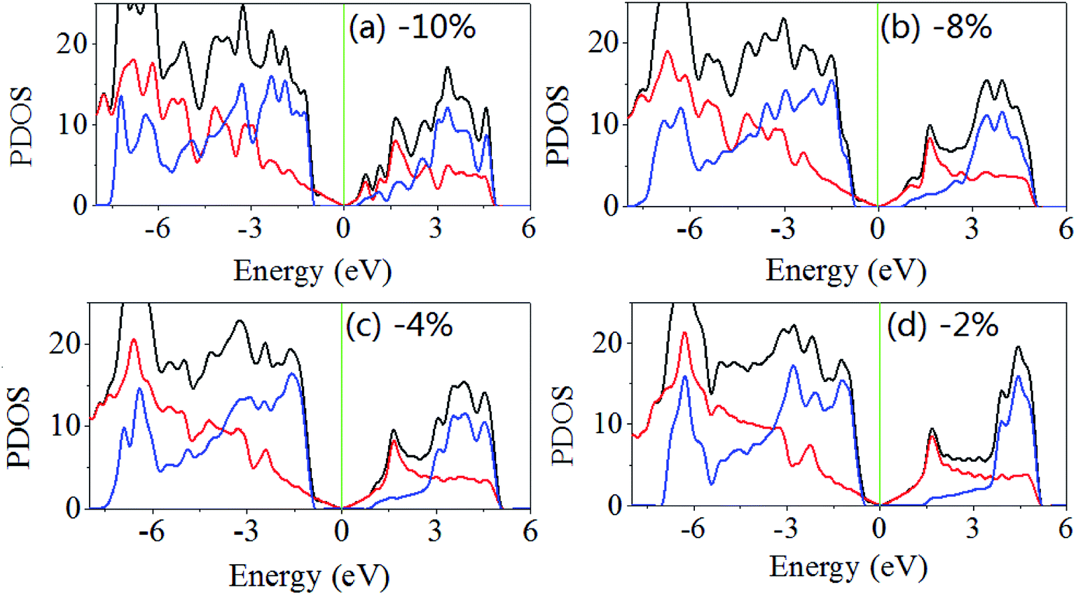
Then, the electronic properties of the GaN/graphene heterostructure are modulated when the uniaxial (x-direction) and biaxial (x- and y-direction) strain are applied. For uniaxial strain, the band gap is reduction with increasing applied strain (both tensile and compressive). As shown in Fig. 4, the band gaps are 1.930, 1.928, 1.900 and 1.814 eV when the uniaxial strains are −2%, −4%, −8% and −10%. It is also found that the Fermi level shifts to near the valence band maximum and away from the conduction band minimum, but the difference between Fermi level and the conduction band minimum maintains larger than that between Fermi level and the valence band maximum. When the uniaxial strains are 2%, 4% and 8%, the band gaps of GaN/graphene heterostructure are 1.915, 1.724 and 1.273 eV. Although the Fermi level shifts to near the conduction band minimum, the difference between Fermi level and the valence band maximum is almost not change with increasing applied the uniaxial tensile strain.
 | ||
| Fig. 4 Density of states the GaN/graphene heterostructure with different applied uniaxial strain along x-direction. The negative value represents the compressive strain. | ||
The same results are obtained when the biaxial strain is applied. As shown in Fig. 5, when the biaxial strains are −2%, −4%, −8% and −10%, the band gaps are 1.896, 1.843, 1.528 and 1.384 eV. The Fermi level shifts to near the valence band maximum and away from the conduction band minimum, and when the biaxial strain less than 8% the difference between Fermi level and the valence band maximum is large than that between Fermi level and the conduction band minimum. When increasing applied the biaxial tensile strain, the difference between Fermi level and the conduction band minimum decreases rapidly but the difference between Fermi level and the valence band maximum changes slightly.
 | ||
| Fig. 5 Density of states of GaN/graphene heterostructure with different applied biaxial strain in-plane (x and y, equally). The negative value represents the compressive strain. | ||
To quantitatively characterize the Schottky barrier height, the evolution of ΦSB,P and ΦSB,N of GaN/graphene heterostructure as function of strain is shown in Fig. 6. The magnitude of ΦSB,P gradually increases and magnitude of ΦSB,N decreases when the uniaxial strain increases to −1%, and then the magnitude of ΦSB,P gradually decreases but magnitude of ΦSB,N are almost not change. Consequently, the value of ΦSB,P is negative when the uniaxial strain is −1%, where the contact type transforms from the p-type Schottky contact to ohmic contact. In contrast, with increasing the biaxial strain, the contact Schottky barrier transforms from n-type transforms from the p-type when the biaxial strain is up to −8%, and then to ohmic contact when the biaxial strain is above 0%.
 | ||
| Fig. 6 Evolution of Schottky barriers of ΦSB,P and ΦSB,N in GaN/graphene heterostructure as a function of the applied strain: (a) uniaxial and (b) biaxial. | ||
4. Conclusions
In conclusion, the structural and electronic properties of GaN/graphene heterostructure are investigated by using first-principles calculation. The results showed that the electronic properties of the GaN/graphene heterostructure are well preserved owing to a weak vdW interaction between GaN and graphene. The SBH in the GaN/graphene heterostructure can be efficiently modulated by applying strain. The band gap of GaN in heterostructure decreases with increasing applied uniaxial and biaxial strains (both tensile and compressive). Moreover, the contact type transforms from the p-type Schottky contact to ohmic contact for GaN/graphene heterostructure with increasing the uniaxial strain, while the contact Schottky barrier transforms from n-type transforms to the p-type and then to ohmic contact with increasing the biaxial strain. These results suggest that graphene can be a very promising material for the metal electrode, and it can enhance the contact performance while still maintaining the electronic properties of GaN.Conflicts of interest
There are no conflicts to declare.Acknowledgements
This work was supported by National Natural Science Foundation of China (Grant No. 51274163), Shanxi Province Key Laboratory Research Project (Grant No. 13JS076), Key Scientific and Technological Innovation Team in Shanxi Province (Grant No. 2012KCT-25), Project of special funds for Key Discipline Project in Shanxi Province (Grant No. 2011HBSZS009).References
- D. Xiao, G. B. Liu, W. X. Feng, X. D. Xu and W. Yao, Phys. Rev. Lett., 2012, 108(19), 196802 CrossRef PubMed.
- Z. Y. Zhu, Y. C. Cheng and U. Schwingenschlogl, Phys. Rev. B: Condens. Matter Mater. Phys., 2011, 84(15), 153402 CrossRef.
- Q. L. Fang, X. M. Zhao, Y. H. Huang, K. W. Xu, T. Min and F. Ma, J. Mater. Chem. C, 2019, 7(12), 3607–3616 RSC.
- M. L. Sun, J.-P. Chou, J. F. Gao, Y. Cheng, A. Hu, W. C. Tang and G. Zhang, ACS Omega, 2018, 3(8), 8514–8520 CrossRef CAS.
- M. L. Sun, J.-P. Chou, L. H. Shi, J. F. Gao, A. Hu, W. C. Tang and G. Zhang, ACS Omega, 2018, 3(6), 5971–5979 CrossRef CAS.
- Q. L. Fang, X. M. Zhao, Y. H. Huang, K. W. Xu, T. Min, P. K. Chu and F. Ma, Phys. Chem. Chem. Phys., 2018, 20(1), 553–561 RSC.
- H. Shu, F. Li, C. Hu, P. Liang, D. Cao and X. Chem, Nanoscale, 2016, 8(36), 2918–2926 RSC.
- S. K. Behera and P. Deb, RSC Adv., 2017, 7(50), 31393–31400 RSC.
- J. E. Padilha, A. Fazzio and A. J. R. da Silva, Phys. Rev. Lett., 2015, 114(6), 066803 CrossRef CAS PubMed.
- H. C. Diaz, J. Avila, C. Y. Chen, R. Addou, M. C. Asensio and M. Batzill, Nano Lett., 2015, 15(2), 1135 CrossRef PubMed.
- H. V. Phuc, N. N. Hieu, B. D. Hoi and C. V. Nguyen, Phys. Chem. Chem. Phys., 2018, 20(26), 17899–17908 RSC.
- P. T. T. Le, N. N. Hieu, L. M. Bui, H. V. Phuc, B. D. Hoi, B. Amin and C. V. Nguyen, Phys. Chem. Chem. Phys., 2018, 20(44), 27856–27864 RSC.
- K. D. Pham, N. N. Bieu, H. V. Phuc, I. A. Fedorov, C. A. Duque, B. Amin and C. V. Nguyen, Appl. Phys. Lett., 2018, 113(17), 171605 CrossRef.
- H. V. Phuc, V. V. Ilyasov, N. N. Hieu, B. Amin and C. V. Nguyen, J. Alloys Compd., 2018, 750(25), 765–773 CrossRef CAS.
- K. Ren, M. L. Sun, Y. Luo, S. Wang, Y. J. Xu, J. Yu and W. C. Tang, Phys. Lett. A, 2019, 383(24), 1487–1492 CrossRef CAS.
- K. Ren, M. L. Sun, Y. Luo, S. Wang, Y. J. Xu, J. Yu and W. C. Tang, Appl. Surf. Sci., 2019, 476(15), 70–75 CrossRef CAS.
- U. Kuhl and H. J. Stöckmann, Phys. Rev. Lett., 1998, 80(15), 3232–3235 CrossRef CAS.
- C. R. Dean, L. Wang, P. Maher, C. Forsythe, F. Ghahari, Y. Gao, J. Katoch, M. Ishigami, P. Moon and M. Koshino, et al., Nature, 2013, 497(7451), 598–602 CrossRef CAS.
- Q. L. Fang, Y. H. Huang, Y. P. Miao, K. W. Xu, Y. Li and F. Ma, J. Phys. Chem. C, 2017, 121(12), 6605–6613 CrossRef CAS.
- Q. L. Fang, X. M. Zhao, Y. H. Huang, K. W. Xu, T. Min, P. K. Chu and F. Ma, J. Mater. Chem. C, 2018, 6(16), 4523–4530 RSC.
- P. Rivera, K. L. Seyler, H. Yu, J. R. Schaibley, J. Yan, D. G. Mandrus, W. Yao and X. Xu, Science, 2016, 351(6274), 688–691 CrossRef CAS PubMed.
- Y. M. Li, J. Li, L. K. Shi, D. Zhang, W. Yang and K. Chang, Phys. Rev. Lett., 2015, 115(15), 166804 CrossRef PubMed.
- S. Pimputkar, J. S. Speck, S. P. DenBaars and S. Nakamura, Nat. Photonics, 2009, 3(4), 180–182 CrossRef CAS.
- E. Kioupakis, P. Rinke, A. Janotti, Q. Yan and C. G. Van de Walle, Energy Conversion: Solid-State Lighting, in Computational Approaches to Energy Materials, ed. A. Walsh, A. A. Sokol and C. R. A. Catlow, John Wiley & Sons Ltd., Oxford, U.K., 2013, pp. 231–259 Search PubMed.
- J. Verma, P. K. Kandaswamy, V. Protasenko, A. Verma, H. Grace Xing and D. Jena, Appl. Phys. Lett., 2013, 102(4), 041103 CrossRef.
- K. Ren, S. K. Wang, Y. Luo, Y. J. Xu, M. L. Sun, J. Yu and W. C. Tang, RSC Adv., 2019, 9(9), 4816–4823 RSC.
- Z. Y. Al Balushi, K. Wang, R. K. Ghosh, R. A. Vila, S. M. Eichfeld, J. D. Caldwell, X. Qin, Y.-C. Lin, P. A. DeSario, G. Stone, S. Subramanian, D. F. Paul, R. M. Wallace, S. Datta, J. M. Redwing and J. A. Robinson, Nat. Mater., 2016, 15(11), 1166–1171 CrossRef CAS.
- G. Kresse and J. Hafner, Phys. Rev. B: Condens. Matter Mater. Phys., 1993, 47(1), 558–561 CrossRef CAS PubMed.
- G. Kresse and J. Hafner, Phys. Rev. B: Condens. Matter Mater. Phys., 1994, 49(20), 14251–14269 CrossRef CAS.
- P. E. Blöchl, Phys. Rev. B: Condens. Matter Mater. Phys., 1994, 50(24), 17953–17979 CrossRef PubMed.
- J. P. Perdew, K. Burke and M. Ernzerhof, Phys. Rev. Lett., 1996, 77(18), 3865–3868 CrossRef CAS PubMed.
- Q. Chen, H. Hu, X. J. Chen and J. L. Wang, Appl. Phys. Lett., 2011, 98(5), 053102 CrossRef.
- S. Grimme, J. Comput. Chem., 2006, 27(15), 1787–1799 CrossRef CAS.
- K. Momma and F. Izumi, J. Appl. Crystallogr., 2008, 41, 653–658 CrossRef CAS.
- K. S. Arunima and G. H. Richard, Appl. Phys. Lett., 2014, 105(5), 051604 CrossRef.
- L. Liu, P. Jewook, A. S. Devid, F. M. Kevin, W. C. Kendal, W. Deng, B. Leonardo, C. I. Juan, A. P. Li and G. Gu, Science, 2014, 343(6167), 163–167 CrossRef CAS PubMed.
- W. Hu, T. Wang, R. Zhang and J. Yang, J. Mater. Chem. C, 2016, 4(9), 1776–1781 RSC.
- J. E. Padilha, A. Fazzio and A. J. R. da Silva, Phys. Rev. Lett., 2015, 114(6), 066803 CrossRef CAS PubMed.
- W. Hu, T. Wang and J. Yang, J. Mater. Chem. C, 2015, 3(18), 4756–4761 RSC.
- B. Liu, L.-J. Wu, Y.-Q. Zhao, L.-Z. Wang and M.-Q. Cai, Phys. Chem. Chem. Phys., 2016, 18(29), 19918–19925 RSC.
- Y. Cai, G. Zhang and Y.-W. Zhang, J. Phys. Chem. C, 2015, 119(11), 13929–13936 CrossRef CAS.
- C. Xia, B. Xue, T. Wang, Y. Peng and Y. Jia, Appl. Phys. Lett., 2015, 107(19), 193107 CrossRef.
- Y. Wang and Y. Ding, Phys. Chem. Chem. Phys., 2015, 17(41), 27769–27776 RSC.
- G. Xiao, L. L. Wang, Q. Y. Rong, H. Q. Xu and W. Z. Xiao, Phys. B, 2017, 524, 47–52 CrossRef CAS.
- J. J. Guo, Z. P. Zhou, T. X. Wang, Z. S. Lu, Z. X. Yang and C. Liu, Curr. Appl. Phys., 2017, 17(12), 1714–1720 CrossRef.
- M. L. Sun, J. P. Chou, Q. Q. Ren, Y. M. Zhao, J. Yu and W. C. Tang, Appl. Phys. Lett., 2017, 110(17), 173105 CrossRef.
| This journal is © The Royal Society of Chemistry 2019 |