
 Open Access Article
 This Open Access Article is licensed under a
 Creative Commons Attribution 3.0 Unported Licence
Electrodeposition of amorphous WO3 on SnO2–TiO2 inverse opal nano-framework for highly transparent, effective and stable electrochromic smart window†
Tam Duy Nguyen*ab,
Loo Pin Yeoab,
Daniel Mandler bc,
Shlomo Magdassibc and
Alfred Iing Yoong Tok*ab
bc,
Shlomo Magdassibc and
Alfred Iing Yoong Tok*ab
aSchool of Materials Science and Engineering, Nanyang Technological University, 50 Nanyang Avenue, Singapore 639798. E-mail: tamnguyen@ntu.edu.sg; MIYTok@ntu.edu
bSingapore-HUJ Alliance for Research and Enterprise, NEW-CREATE Phase II, Campus for Research Excellence and Technological Enterprise (CREATE), Singapore 138602
cInstitute of Chemistry, The Hebrew University of Jerusalem, Jerusalem 9190401, Israel
First published on 29th May 2019
Abstract
In recent years, there has been significant advancement in smart window technologies due to their effectiveness in reducing energy consumption of indoor lighting and air-conditioning in buildings. Electrochromic (EC) materials, in particular, have been widely studied as they provide a simple method for tuning or modulating visible light and infrared (IR) transmittance. In this work, a novel hybrid, multi-layered SnO2–TiO2–WO3 inverse opal (IO) nanostructure has been fabricated via dip-coating and electrodeposition process. This hybrid nanostructure allows an electrochromic smart window for effective near infrared (NIR) modulation, with high visible transparency and durable EC cycling stability. The visible transparency of as-fabricated hybrid multi-layered SnO2–TiO2–WO3 IO was measured to be in the range of 67.2–88.0% in the bleached state and 67.0–74.4% in the colored state, respectively. Furthermore, the hybrid nanostructure is also able to modulate up to 63.6% NIR radiation at the wavelength of 1200 nm and maintain approximately 82.6% of its NIR blockage capability after 750 reversible cycles. The hybrid multi-layered SnO2–TiO2–WO3 IO nanostructure in this study can potentially be an effective and stable EC material for advanced smart window technology.
Introduction
Electrochromic (EC) materials are defined by their ability to change their optical properties reversibly through the application of an electrical current or voltage.1,2 Many promising applications that have been proposed, e.g. smart glass, electrochromic mirrors, and electrochromic display devices, rely on the phenomenon of electrochromism. EC smart window technology, which is able to electrically modulate the transmittance of solar radiation, is one of the most widely investigated methods to assist in the reduction of energy consumption in indoor lighting and air-conditioning.3 This is especially relevant now as more high-rise buildings, are placing enormous strains on energy demands for indoor cooling and heating. Amongst the various EC materials, transition metal oxide WO3 is one of the earliest studied materials and still possesses the best EC performance to date.1 Upon the electrochemical insertion/extraction of small cations such as H+ or Li+, WO3 exhibits corresponding reversible changes in optical property (colored/bleached) (eqn (1), M = H, Li,…):4–8| [WO3 + M+ + e−]bleached ↔ [MWO3]colored | (1) |
Various material structures and designs have been investigated to improve the overall EC performance of WO3, such as nanoparticles,9–15 thin films,16–26 nanorods27–29 etc. The crystal structure of WO3 is also another factor affecting the performance, with many studies reporting that amorphous WO3 has better EC efficiency than its crystalline form due to higher ion storage capacity at the same applied voltage.30–34 Recently, a modification technique based on three-dimensional inverse opal (IO) structures has been widely used to improve the overall performance of WO3 EC material, owing to an enhancement in light absorption with its continuous and periodic structure. In addition, its large specific surface area also increases the active area and improves charge transfer kinetics during redox reactions.35–41
Since the high visible transparency is one of the fundamental properties of glass window, it is necessary to shift the radiation modulation to the IR (or NIR) range. On the other hand, the IR (or NIR) modulation is also found to be more effective for the heat management in the field of smart window, as nearly 50% of solar energy comes from IR radiation. However, many studies on WO3 EC materials have achieved a large IR (or NIR) modulation, but have failed to get high visible transparency especially in the colored state. For example, Zhou et al. reported Ag/WO3 nanowires which enable approximately 59% NIR modulation at 1100 nm, and approximately 57.1% transparency at 500 nm.26 The bilayer WO3 IO structure synthesized by Li et al. showed 57.6% NIR modulation at 1100 nm, but only 27.3% transparency at 500 nm.40 The hybrid TiO2–WO3 IO structure synthesized by Ling et al. also achieved about 62.5% NIR modulation at 1100 nm, but only 22.7% transparency at 500 nm.41 The second issue that the WO3-based smart window system needs to overcome is the low device lifespan. Long-term EC performance of WO3 materials is found to be suffered from degradation due to the accumulation of trapped ions in the host structure.42–47 To improve the stability, many modification methods have been reported, including tuning of the fabrication process,48 optimizing periodicity and degree of crystallinity,49 and varying of the film thickness.50 Wen et al. reported that ion-trapping-induced degradation, which is commonly believed to be irreversible, can be successfully eliminated by constant current-driven de-trapping.51 However, doping or compositing with metal cations or metal oxides, e.g. Nb,52 Mo,53 and most commonly with Ti,41,54–60 are the most effective methods to improve EC cycle stability of WO3. Overall, it is still a challenge to develop an optimal material structure and design that can satisfy all requested features of a modern smart window technology, e.g. high visible transparency, effective NIR modulation and long-term EC stability.
In this study, we aim to achieve all such features in a WO3-based nanostructure using double-layered SnO2–TiO2 IO framework to produce a multi-layered structure. The polystyrene (PS) opal was used as the initial template to fabricate the SnO2 and SnO2–TiO2 IO framework, after which the electrodeposition method was employed to obtain the hybrid multi-layered SnO2–TiO2–WO3 IO nanostructures. The morphology, crystal structure and surface chemistry of the as-fabricated multi-layered SnO2–TiO2–WO3 IO nanostructures were characterized by Field Emission Scanning Electron Microscopy (FESEM), X-ray diffraction (XRD), Scanning Transmission Electron Microscopy (STEM) coupled with energy-dispersive X-ray spectroscopy (EDX), and X-ray photoelectron spectrometer (XPS), respectively. The optical properties and NIR modulation performance of hybrid multi-layered SnO2–TiO2–WO3 IO nanostructures were examined by Ultraviolet-Visible-NIR (UV-Vis-NIR) spectroscopy under constant potential supply. It was found that the addition of an ultra-thin TiO2 layer on SnO2 IO framework could effectively improve the long-term EC cycling stability of SnO2–TiO2–WO3 IO nanostructure, while maintaining the effective NIR modulation and high visible transparency in both the colored and bleached states. This study introduces a novel EC material structure for stable and effective NIR-active smart window applications.
Experimental
Synthesis of hybrid multi-layered SnO2–TiO2–WO3 inverse opal
Fig. S1† illustrates the fabrication procedure of hybrid multi-layered SnO2–TiO2–WO3 IO nanostructure. Mono-dispersed polystyrene (PS) spheres (Thermo Fisher Scientific) were diluted in DI water and sonicated for 30 min. Clean FTO glasses (1.5 × 2.5 cm2) were immersed in the PS dispersion horizontally at 60 °C for 3 days to achieve a self-assembled PS opal template on the FTO glass substrate. In this work, two initial PS opal sizes were used in the fabrication process (392 and 520 nm).The SnO2 IO was obtained by dip-coating the PS opal template in an aqueous SnO2 precursor.61 The precursor solution was prepared by mixing 15 mL of ethylene glycol (EG) (Sigma-Aldrich) and 3 mmol of SnCl4·5H2O (Sigma-Aldrich) in a glass beaker under continuous stirring, then heated up to 120 °C for 1 h. After cooling of the mixture, 35 mL of ethanol (Sigma-Aldrich) was added into the solution to reduce the viscosity. The PS opal template was dipped twice into the resultant solution under vacuum for 3 min each time and left to dry at 60 °C for 20 min. Vacuum dipping, in this case, assisted the infiltration of the precursor into the PS opal structure. This was followed by calcination at 500 °C for 2 h (ramping rate 1 °C min−1) to obtain the SnO2 IO. Similarly, a thin TiO2 layer was deposited onto the SnO2 IO surface by dipping into the TiO2 precursor. The standard recipe of the TiO2 precursor solution for the dip-coating process was prepared by mixing 1 mL of titanium tetra-butoxide (Sigma-Aldrich), 0.4 mL of hydrochloric acid (37%, Sigma-Aldrich), 16 mL of ethanol (Sigma-Aldrich), and 10 mL of DI water, respectively. The SnO2 IO framework was vacuum-dipped into the precursor solution once for 45 seconds and then dried at 60 °C for 20 min. The dip-coated samples were heated at 500 °C for 2 hours at a heating rate of 1 °C min−1 to obtain the double-layered SnO2–TiO2 IO framework.
Finally, WO3 electrodeposition was carried out on the SnO2–TiO2 IO structure to fabricate the hybrid multi-layered SnO2–TiO2–WO3 IO nanostructure. The WO3 precursor solution was prepared by mixing 1.03 g of Na2WO4·2H2O (Sigma-Aldrich) and 0.65 mL of H2O2 (Sigma-Aldrich) in 250 mL of DI water. After that, 2 mL of HClO4 (Sigma-Aldrich) was gradually added into the solution until the pH reached the value of 1.2.62 The electrodeposition process was conducted at a constant potential of −0.7 V for 200 seconds. SnO2–WO3 and TiO2–WO3 IO nanostructures were also prepared as the references using the same parameters. The obtained samples were rinsed with DI water and dried with nitrogen gas.
Characterization
The morphologies of the obtained samples were characterized by FESEM (JEOL 7600F). The crystal structure of SnO2–TiO2–WO3 IO was characterized by an X-ray diffractometer (Shimadzu XRD-6000, with the λ Cu-Kα = 0.15418 nm). The atomic compositions and core–shell structure were identified by a STEM (JEOL 2100F STEM equipped with INCA EDS detector). The surface chemistry is characterized by a Kratos AXIS Supra X-ray photoelectron spectrometer.The spectro-electrochemical properties of obtained samples were measured using a Solartron potentiostat (Model 1470E) and a UV-Vis-NIR spectrophotometer (Shimadzu UV 3600). The UV-Vis spectra of all samples were recorded in the wavelength range of 300 to 1600 nm at potentials of −0.3 and +0.8 V. The dynamic optical transmittance was also recorded for the SnO2–TiO2–WO3 IO samples in the wavelength range of interest under repeating square wave potentials oscillating between +0.8 and −0.3 V at a time step of 120 s and 80 s respectively. It was recorded for more than 750 reversible cycles to characterize its long-term stability.
Results and discussion
Morphology, crystal structure and surface chemistry
Fig. 1 shows the FESEM images of as-synthesized SnO2, SnO2–TiO2 and hybrid multi-layered SnO2–TiO2–WO3 IO nanostructure with initial PS opal size of 392 nm. The SnO2 IO framework (Fig. 1a) is homogenously fabricated after the removal of PS template. The diameter of the SnO2 IO pores is approximately 250 nm, which is smaller than that of the initial PS opal diameter (392 nm) due to shrinkage in the SnO2 framework following the calcination process at 500 °C. The SnO2 IO framework is arranged in a hexagonal array and the openings that connect the adjacent pores can be clearly observed. The distance between two adjacent pores is measured to be approximately 260 nm. With the coating of a thin layer of TiO2, there is no significant change in the morphology of the double-layered SnO2–TiO2 IO framework (Fig. 1b). However, following WO3 electrodeposition, a uniformly deposited WO3 layer can be clearly observed on the surface of the double-layered SnO2–TiO2 IO framework (Fig. 1c), forming a hybrid multi-layered SnO2–TiO2–WO3 IO nanostructure. The HRTEM image also confirms the inverse opal structure of as-fabricated SnO2–TiO2–WO3 nanostructures, with the void space of SnO2 framework approximated at 270 nm (Fig. 1d). Samples fabricated from 520 nm initial PS opal template have similar morphologies to the 392 nm samples, except with bigger void space dimensions (Fig. S2†). | ||
| Fig. 1 FESEM images of SnO2 IO (a), SnO2–TiO2 IO (b), and hybrid multi-layered SnO2–TiO2–WO3 IO nanostructure (c) with initial pore-size of 392 nm and electro-deposition duration of 200 seconds. All images were acquired under the same magnification. (d) HRTEM image of hybrid multi-layered SnO2–TiO2–WO3 IO nanostructure. | ||
Fig. 2 shows the XRD patterns of FTO substrate, SnO2 IO, TiO2 IO and hybrid multi-layered SnO2–TiO2–WO3 IO samples. It is observed that both FTO substrate and SnO2 IO exhibit characteristic diffraction peaks at 2θ = 26.7, 33.8, 38.0, 51.7, 55.0, 61.7, 66.1, 78.7°, which correspond to the planes of (110), (101), (200), (211), (220), (310), (301) and (321) of SnO2 (ICDD 01-070-4176), respectively. There is a dissimilarity in the (200) plane peak intensity of both samples, which may be due to the different preferred crystal orientation in SnO2 IO structure as compared to the bare FTO glass. The XRD pattern of TiO2 IO indicates the formation of anatase TiO2, with characteristic diffraction peaks at 2θ = 25.4, 37.9, 48.1, 54.0, 62.8°, corresponding to the planes of (101), (004), (200), (105), and (211) of TiO2 (ICDD 96-101-0943), respectively. The XRD pattern of multi-layered SnO2–TiO2–WO3 IO shows only the formation of SnO2 and TiO2 crystal with a lack of distinct WO3 peaks, which implies the amorphous nature of the electrodeposited WO3 layer.
 | ||
| Fig. 2 XRD patterns of FTO, SnO2 IO, TiO2 IO and hybrid multi-layered SnO2–TiO2–WO3 IO nanostructure. | ||
The STEM image coupled with EDX mapping, as shown in Fig. 3a, reveals the multi-layered structure of as-fabricated SnO2–TiO2–WO3 IO. The distribution of SnO2, TiO2 and WO3 layers can be observed in the multi-layered IO nanostructure mapping, which clearly shows that the inner SnO2–TiO2 framework is surrounded by a layer of amorphous WO3. As shown in Fig. 3b, the bulk elemental composition of as-fabricated SnO2–TiO2–WO3 IO is measured to be 53.9, 5.0 and 41.1 at% for Sn, Ti and W, respectively. This indicates that the thickness of the TiO2 layer is very thin as compared to the SnO2 and WO3 layers.
 | ||
| Fig. 3 STEM images coupled with EDX mapping of hybrid multi-layered SnO2–TiO2–WO3 IO nanostructure (a) and bulk elemental composition obtained from EDX analysis. | ||
The surface chemistry of hybrid multi-layered SnO2–TiO2–WO3 IO nanostructure is characterized by XPS measurement. Fig. 4 presents the wide scan XPS spectra and surface elemental compositions of SnO2–WO3, TiO2–WO3 and hybrid multi-layered SnO2–TiO2–WO3 IO nanostructures. The wide scan spectra (Fig. 4a) demonstrate the presence of O1s, W4f and Sn3d peaks in all samples, while the peak of Ti2p is negligible due to the low content of TiO2 as mentioned in the above EDX bulk analysis. By quantification analysis, the surface elemental composition of SnO2–WO3 IO is composed of approximately 1.3, 25.4 and 73.3 at% of Sn, W and O, respectively. For TiO2–WO3 IO, this value is 0.8, 27.2 and 72.0 at% for Ti, W and O, respectively. For hybrid multi-layered SnO2–TiO2–WO3 IO, it is measured to be about 0.1, 0.3, 17.2 and 82.4 at% for Sn, Ti, W and O, respectively. The higher amount of W as compared to Sn and Ti reveals the dominance of WO3 layer on the surface of hybrid multi-layered SnO2–TiO2–WO3 IO. The bulk EDX analysis, however, shows that the amount of W (41.1 at%) and Ti (5 at%) is much lower than Sn (53.9 at%) in the hybrid multi-layered SnO2–TiO2–WO3 IO. The results of both analyses correspond well with the expected arrangement in the multi-layered structure of hybrid SnO2–TiO2–WO3 IO.
 | ||
| Fig. 4 Wide scan XPS spectra (a) and surface elemental composition (b) of SnO2–WO3, TiO2–WO3, and hybrid multi-layered SnO2–TiO2–WO3 IO nanostructure. | ||
Fig. 5 presents the fine scan XPS spectra of O1s, W4f, Ti2p and Sn3d components of hybrid multi-layered SnO2–TiO2–WO3 IO. By curve-fitting analysis, the O1s spectrum of hybrid SnO2–TiO2–WO3 IO is located in the metal oxide binding energy range (∼530.8 eV). The W4f spectrum is located at the binding energy of approximately 36.0 eV, confirming the WO3 chemical state, with well separated spin–orbit components (Δmetal = 2.17 eV). The Ti2p spectrum also confirms the TiO2 chemical state (∼459.1 eV). The fine scan XPS spectra of SnO2–WO3 and TiO2–WO3 IO nanostructure can also be found in the ESI (Fig. S4).†
 | ||
| Fig. 5 The fine XPS spectra of O1s (a), W4f (b), Ti2p (c), and Sn3d (d) components of hybrid multi-layered SnO2–TiO2–WO3 IO nanostructure. | ||
Optical properties and NIR modulation performance
Since FTO glass allows less than 30% IR transmittance beyond 1600 nm, this work will focus only on the NIR modulation within the range of 700–1600 nm, while the visible transparency is examined between 300–700 nm.41,61 Fig. 6 shows the UV-Vis spectra of SnO2–WO3, TiO2–WO3 and hybrid multi-layered SnO2–TiO2–WO3 IO recorded at constant potentials of +0.8 V and −0.3 V from 300 to 1600 nm in 0.1 M LiClO4/PC electrolyte. It has been reported that the WO3 IO structure has much higher electrochromic performance than that of WO3 thin film.41,61 Therefore, in this work, only IO structures obtained from initial PS sizes of 392 (Fig. 6a) and 520 nm (Fig. 6b) are characterized. In the bleached state, all IO samples demonstrate high transmittance in both NIR and visible regions. Upon applying a negative voltage in the colored state (−0.3 V), all samples show a significant reduction in NIR transmittance while maintaining highly transparent in the visible region. The ability to modulate NIR transmittance over a wide range while remaining transparent satisfies the desired optical properties of hybrid multi-layered SnO2–TiO2–WO3 IO for smart window applications. For both tested pore sizes, the visible transparency of hybrid multi-layered SnO2–TiO2–WO3 IO is mostly similar to SnO2–WO3 IO, and significantly higher than that of TiO2–WO3 IO. | ||
| Fig. 6 UV-Vis-NIR spectra of SnO2–WO3, TiO2–WO3, and hybrid multi-layered SnO2–TiO2–WO3 IO nanostructure at bleached and colored state in 0.1 M LiClO4/PC electrolyte. Each UV-Vis-NIR spectrum is obtained from the average of three independent scans. | ||
The detailed electrochromic performance of SnO2–WO3, TiO2–WO3 and hybrid multi-layered SnO2–TiO2–WO3 IO nanostructures are presented in the UV-Vis spectra in Fig. 7. Data at several wavelengths were specifically selected for better comparison of the modulation effect: 400, 500, 600 nm (Fig. 7a and b) in the visible region and 800, 1200, 1600 nm (Fig. 7c and d) in the NIR region. In Fig. 7a, 392 nm SnO2–WO3 IO indicates a visible transparency of 70.8–89.8% during the bleached state and 62.2–70.0% during the colored state. The transparency of 392 nm TiO2–WO3 IO is lower at 54.6–78.2% during the bleached state and only 52.8–56.7% during the colored state. The hybrid multi-layered SnO2–TiO2–WO3 IO shows a similar transparency as SnO2–WO3 IO: 67.2–88.0% in the bleached and 67.0–74.4% in the colored states. The same trend of visible transparency was observed for all samples of 520 nm initial PS opal size (Fig. 7b). In comparison with other research, the visible transparency of as-fabricated hybrid multi-layered SnO2–TiO2–WO3 IO nanostructure is found to be much higher, especially in the colored state. Zhou et al. reported Ag/WO3 nanowires with approximately 57.1% transparency at 500 nm.26 The bilayer WO3 IO structure synthesized by Li et al. showed only 27.3% transparency at 500 nm.40 The hybrid TiO2–WO3 IO structure synthesized by Ling et al. also achieved only 22.7% transparency at 500 nm.41 This significant improvement in visible light transparency is due to the excellent optical transparency of the SnO2 framework as compared to TiO2.
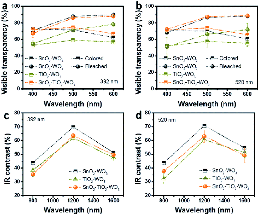 | ||
| Fig. 7 Visible transparency (a and b) and NIR contrast (c and d) between colored and bleached state of SnO2–WO3, TiO2–WO3, and hybrid multi-layered SnO2–TiO2–WO3 IO nanostructure. | ||
The NIR contrast between the bleached and colored states of SnO2–WO3, TiO2–WO3 and hybrid multi-layered SnO2–TiO2–WO3 IO nanostructures is presented in Fig. 7c and d. In general, the SnO2–WO3 IO demonstrates the highest NIR modulation capability, while the hybrid multi-layered SnO2–TiO2–WO3 IO reveals better NIR modulation than the TiO2–WO3 IO. The 392 nm SnO2–WO3 IO (Fig. 7c) shows 44.0, 69.7 and 51.2% NIR modulation at 800, 1200 and 1600 nm respectively while TiO2–WO3 IO shows 38.5, 61.2 and 47.5% NIR modulation at 800, 1200 and 1600 nm, respectively. For the hybrid multi-layered SnO2–TiO2–WO3 IO, the NIR modulation is recorded to be approximately 35.5, 63.6 and 49.6% at 800, 1200 and 1600 nm, respectively. For the samples with 520 nm initial PS opal size (Fig. 7d), the NIR contrast at 800, 1200 and 1600 nm is measured to be 43.8, 70.7 and 54.6% for SnO2–WO3 IO, 32.1, 60.6 and 51.2% for TiO2–WO3 IO, about 37.8, 63.1 and 49.1% for hybrid multi-layered SnO2–TiO2–WO3 IO, respectively. The results imply that the NIR modulation performance of SnO2–WO3 IO structure is not influenced by the presence of an ultra-thin TiO2 layer on SnO2 surface. In comparison with other reports, as-fabricated hybrid multi-layered SnO2–TiO2–WO3 IO demonstrates comparable NIR modulation performance. The Ag/WO3 nanowires reported by Zhou et al. showed approximately 59% NIR modulation at 1100 nm;26 the bilayer WO3 IO structure synthesized by Li et al. showed approximately 57.6% NIR modulation.40 The hybrid multi-layered SnO2–TiO2–WO3 IO demonstrated 56.9 and 57.6% NIR modulation at 1100 nm for 392 and 520 nm initial PS opal sizes, respectively. Therefore, the hybrid multi-layered SnO2–TiO2–WO3 IO nanostructure developed in this study can provide two promising advantages in the smart windows technology: (1) large thermal radiation modulation and (2) high visible transparency. These advantages will be beneficial for the optimization of in-door lighting and thermal management.
The electro-optical response time in switching between the bleached and colored states of SnO2–WO3, TiO2–WO3 and hybrid multi-layered SnO2–TiO2–WO3 IO nanostructures is presented in Fig. 8a–c. The switching time is recorded to be approximately 21.6 and 21.1 s for the SnO2–WO3 and TiO2–WO3 IO, respectively. The switching time taken for the hybrid multi-layered SnO2–TiO2–WO3 IO is slightly longer, i.e. 24.5 s. Fig. 8d–f show the UV-Vis kinetics spectra of SnO2–WO3, TiO2–WO3 and hybrid multi-layered SnO2–TiO2–WO3 IO at 1033 nm for 750 reversible cycles. The electrochromic capacity of SnO2–WO3 IO was found to reduce gradually over 750 cycles for both the bleached and colored states. It is estimated that the electrochromic performance reduces by 9.3 and 35.6% in the bleached and colored states, respectively. The electrochromic cycling stability of TiO2–WO3 IO shows improvement, with only 4.7 and 21.4% reduction in stability in the bleached and colored states respectively after 750 cycles. The novel hybrid multi-layered SnO2–TiO2–WO3 IO indicates the most significant improvement in EC stability. After 750 cycles, only 1.5 and 19.4% reduction in stability were recorded during the bleached and colored states, respectively. These results suggest that the presence of a thin TiO2 layer on SnO2 IO framework can significantly improve EC stability, and thus maintain the NIR modulation capability in hybrid multi-layered SnO2–TiO2–WO3 IO nanostructure.
 | ||
| Fig. 8 Electro-optical response time between bleached and colored state (a–c) and kinetics stability (d–f) of SnO2–WO3, TiO2–WO3, and hybrid multi-layered SnO2–TiO2–WO3 IO nanostructure for over 750 cycles. | ||
It was reported that lithium accumulates as OLi in the WO3 films, but such phenomenon does not occur in WO3–TiO2 films.54 This ion-trapping may be the cause of degradation in the electrochromic performance during bleaching of WO3-based EC materials. Consequently, there is an improved EC stability in TiO2–WO3 structures. In the current study, the results in Fig. 8d–f indicate that the kinetics of ion extraction process (bleached state) is stable for over 750 cycles and only the ion insertion process (colored state) is affected. This implies that there is a reduction in the amount of Li+ ions that can be intercalated into the SnO2–WO3 IO structure after each cycle. This may due to the crystallization of amorphous WO3 layer following the reversible cycling test as observed in a previous study.61 Arvizu et al. also reported that the addition of Ti significantly promoted the amorphous nature of the films and stabilized their electrochemical cycling performance and dynamic range for electrochromism.56 This could be the origin for the stable EC performance of as-fabricated hybrid multi-layered SnO2–TiO2–WO3 IO.
Conclusions
In this work, a novel hybrid multi-layered SnO2–TiO2–WO3 inverse opal (IO) nanostructure is fabricated as an EC material for smart window application via electrodeposition of amorphous WO3 on a double-layered SnO2–TiO2 IO framework. The as-fabricated hybrid nanostructure integrates the high visible transparency of SnO2, effective near infrared (NIR) modulation of amorphous WO3, and durable EC cycling stability of TiO2. It is measured that the novel hybrid multi-layered SnO2–TiO2–WO3 IO is able to modulate up to 63.6% NIR radiation at the wavelength of 1200 nm, while still allowing high visible transparency of approximately 67.2–88.0% and 67.0–74.4% in the bleached and colored states, respectively. Furthermore, it can also maintain approximately 82.6% of its NIR blockage capability after 750 reversible cycles. The smart window technology based on this hybrid multi-layered SnO2–TiO2–WO3 IO nanostructure WO3 can effectively assist in light and thermal management in buildings, thus reducing energy consumption of indoor lighting and air-conditioning.Conflicts of interest
There are no conflicts to declare.Acknowledgements
This research is supported by grants from the National Research Foundation, Singapore under its Campus of Research Excellence and Technological Enterprise (CREATE) Program.Notes and references
- C. G. Granqvist, Handbook of Inorganic Electrochromic Materials, Elsevier, 1st edn., 1995 Search PubMed
.
- Electrochromic Materials and Devices, ed. R. J. Mortimer, D. R. Rosseinsky and P. M. S. Monk, Wiley-VCH, 2015 Search PubMed
- C. G. Granqvist, Thin Solid Films, 2014, 564, 1–38 CrossRef CAS
- A. Hjelm, C. G. Granqvist and J. M. Wills, Phys. Rev. B: Condens. Matter Mater. Phys., 1996, 54, 2436–2445 CrossRef CAS PubMed
- G. A. de Wijs and R. A. de Groot, Phys. Rev. B: Condens. Matter Mater. Phys., 1999, 60, 16463–16474 CrossRef CAS
- N. Bondarenko, O. Eriksson and N. V. Skorodumova, Phys. Rev. B: Condens. Matter Mater. Phys., 2015, 92, 165119 CrossRef
- C. A. Triana, C. G. Granqvist and G. A. Niklasson, J. Appl. Phys., 2015, 118, 024901 CrossRef
- H. Hamdi, E. K. H. Salje, P. Ghosez and E. Bousquet, Phys. Rev. B, 2016, 94, 245124 CrossRef
- H. Takeda and K. Adachi, J. Am. Ceram. Soc., 2007, 90, 4059–4061 CAS
- M. Layani, P. Darmawan, W. L. Foo, L. Liu, A. Kamyshny, D. Mandler, S. Magdassi and P. S. Lee, Nanoscale, 2014, 6, 4572–4576 RSC
- S. Y. Lee, J. Y. Kim, J. Y. Lee, H. J. Song, S. Lee, K. H. Choi and G. Shin, Nanoscale Res. Lett., 2014, 9, 294 CrossRef PubMed
- E. L. Runnerstrom, A. Llordés, S. D. Lounis and D. J. Milliron, Chem. Commun., 2014, 50, 10555–10572 RSC
- H. Ling, L. Liu, P. S. Lee, D. Mandler and X. Lu, Electrochim. Acta, 2015, 174, 57–65 CrossRef CAS
- H. Ling, G. Ding, D. Mandler, P. S. Lee, J. Xu and X. Lu, Chem. Commun., 2016, 52, 9379–9382 RSC
- B. Zhou, W. Feng, G. Gao, G. Wu, Y. Chen and W. Li, Mater. Res. Express, 2017, 4, 115702 CrossRef
- J. S. E. M. Svensson and C. G. Granqvist, Thin Solid Films, 1985, 126, 31–36 CrossRef CAS
- S. Morandi, G. Ghiotti, A. Chiorino and E. Comini, Thin Solid Films, 2005, 490, 74–80 CrossRef CAS
- S. R. Bathe and P. S. Patil, Sol. Energy Mater. Sol. Cells, 2007, 91, 1097–1101 CrossRef CAS
- A. Karuppasamy and A. Subrahmanyam, Thin Solid Films, 2007, 516, 175–178 CrossRef CAS
- M. B. Johansson, B. Zietz, G. A. Niklasson and L. Österlund, J. Appl. Phys., 2014, 115, 213510 CrossRef
- H. Ling, J. Lu, S. Phua, H. Liu, L. Liu, Y. Huang, D. Mandler, P. S. Lee and X. Lu, J. Mater. Chem. A, 2014, 2, 2708–2717 RSC
- Y. Xin, H. Zhou, X. Ni, Y. Pan, X. Zhang, J. Zheng, S. Bao and P. Jin, RSC Adv., 2015, 5, 57757–57763 RSC
- V. R. Buch, A. K. Chawla and S. K. Rawal, Mater. Today: Proc., 2016, 3, 1429–1437 Search PubMed
- M. Meenakshi, R. Sivakumar, P. Perumal and C. Sanjeeviraja, AIP Conf. Proc., 2016, 1731, 080070 CrossRef
- G. Cai, P. Darmawan, X. Cheng and P. S. Lee, Adv. Energy Mater., 2017, 7, 1602598 CrossRef
- K. Zhou, H. Wang, S. Zhang, J. Jiu, J. Liu, Y. Zhang and H. Yan, J. Mater. Sci., 2017, 52, 12783–12794 CrossRef CAS
- J. Wang, E. Khoo, P. S. Lee and J. Ma, J. Phys. Chem. C, 2009, 113, 9655–9658 CrossRef CAS
- J. Zhang, J.-p. Tu, G.-h. Du, Z.-m. Dong, Y.-s. Wu, L. Chang, D. Xie, G.-f. Cai and X.-l. Wang, Sol. Energy Mater. Sol. Cells, 2013, 114, 31–37 CrossRef CAS
- C.-H. Lu, M. H. Hon, C.-Y. Kuan and I.-C. Leu, Jpn. J. Appl. Phys., 2014, 53, 06JG08 CrossRef CAS
- H. R. Zeller and H. U. Beyeler, Appl. Phys., 1977, 13, 231–237 CAS
- S. Hashimoto and H. Matsuoka, J. Appl. Phys., 1991, 69, 933–937 CrossRef CAS
- A. A. Joraid, Curr. Appl. Phys., 2009, 9, 73–79 CrossRef
- M. M. El-Nahass, M. M. Saadeldin, H. A. M. Ali and M. Zaghllol, Mater. Sci. Semicond. Process., 2015, 29, 201–205 CrossRef CAS
- G. Yuan, C. Hua, L. Huang, C. Defranoux, P. Basa, Y. Liu, C. Song and G. Han, Appl. Surf. Sci., 2017, 421, 630–635 CrossRef CAS
- S.-L. Kuai, G. Bader and P. V. Ashrit, Appl. Phys. Lett., 2005, 86, 221110 CrossRef
- L. Liu, S. K. Karuturi, L. T. Su, Q. Wang and A. I. Y. Tok, Electrochem. Commun., 2011, 13, 1163–1165 CrossRef CAS
- H.-N. Kim, H. Yoo and J. H. Moon, Nanoscale, 2013, 5, 4200–4204 RSC
- H. Zhang, G. Duan, G. Liu, Y. Li, X. Xu, Z. Dai, J. Wang and W. Cai, Nanoscale, 2013, 5, 2460–2468 RSC
- P. Labouchere, A. K. Chandiran, T. Moehl, H. Harms, S. Chavhan, R. Tena-Zaera, M. K. Nazeeruddin, M. Graetzel and N. Tetreault, Adv. Energy Mater., 2014, 4, 1400217 CrossRef
- H. Li, J. F. Wang, G. Vienneau, G. B. Zhu, X. G. Wang, J. Robichaud, B.-L. Su and Y. Djaoued, RSC Adv., 2017, 7, 46406–46413 RSC
- H. Ling, L. P. Yeo, Z. Wang, X. Li, D. Mandler, S. Magdassi and A. I. Y. Tok, J. Mater. Chem. C, 2018, 6, 8488–8494 RSC
- J. P. Randin, J. Electron. Mater., 1978, 7, 47–63 CrossRef CAS
- D. Chatzikyriakou, N. Krins, B. Gilbert, P. Colson, J. Dewalque, J. Denayer, R. Cloots and C. Henrist, Electrochim. Acta, 2014, 137, 75–82 CrossRef CAS
- R. Todo, Y. Abe, M. Kawamura and K. H. Kim, ECS Trans., 2014, 58, 125–129 CrossRef
- V. Kotok,
 , V. Solovov and O. Yurlova, Technology Audit and Production Reserves, 2017, 3, 6 CrossRef
 - K. Zhou, H. Wang, J. Liu and H. Yan, Int. J. Electrochem. Sci., 2018, 13, 7335–7346 CrossRef CAS
- Z. Guo, Y. Chen and N. L. Lu, Multifunctional Nanocomposites for Energy and Environmental Applications, Wiley-VCH, Weinheim, 2018 Search PubMed
- J. Yuan, B. Wang, H. Wang, Y. Chai, Y. Jin, H. Qi and J. Shao, Appl. Surf. Sci., 2018, 447, 471–478 CrossRef CAS
- S. Sallard, T. Brezesinski and B. M. Smarsly, J. Phys. Chem. C, 2007, 111, 7200–7206 CrossRef CAS
- K. D. Lee, J. Korean Phys. Soc., 2001, 38, 33–37 CAS
- R.-T. Wen, C. G. Granqvist and G. A. Niklasson, Nat. Mater., 2015, 14, 996 CrossRef CAS PubMed
- S. R. Bathe and P. S. Patil, J. Phys. D: Appl. Phys., 2007, 40, 7423–7431 CrossRef CAS
- J. M. O. R. de León, D. R. Acosta, U. Pal and L. Castañeda, Electrochim. Acta, 2011, 56, 2599–2605 CrossRef
- S. Hashimoto and H. Matsuoka, J. Electrochem. Soc., 1991, 138, 2403–2408 CrossRef CAS
- Y.-C. Nah, A. Ghicov, D. Kim, S. Berger and P. Schmuki, J. Am. Chem. Soc., 2008, 130, 16154–16155 CrossRef CAS PubMed
- M. A. Arvizu, C. A. Triana, B. I. Stefanov, C. G. Granqvist and G. A. Niklasson, Sol. Energy Mater. Sol. Cells, 2014, 125, 184–189 CrossRef CAS
- S. R. Bathe and P. S. Patil, J. Mater., 2014, 2014, 5 Search PubMed
- G. Yang, PhD, National University of Singapore, 2015
- T. Kuroki, Y. Matsushima and H. Unuma, J. Asian Ceram. Soc., 2016, 4, 367–370 CrossRef
- M. D. Peng, Y. Z. Zhang, L. X. Song, L. N. Wu, Y. L. Zhang and X. F. Hu, Surf. Eng., 2017, 33, 305–309 CrossRef CAS
- T. D. Nguyen, L. P. Yeo, T. C. Kei, D. Mandler, S. Magdassi and A. I. Y. Tok, Adv. Opt. Mater., 2019, 7, 1801389 CrossRef
- G. Cai, M. Cui, V. Kumar, P. Darmawan, J. Wang, X. Wang, A. Lee-Sie Eh, K. Qian and P. S. Lee, Chem. Sci., 2016, 7, 1373–1382 RSC

Footnote |
| † Electronic supplementary information (ESI) available: Additional characterization data. See DOI: 10.1039/c9ra03084k |
| This journal is © The Royal Society of Chemistry 2019 |