DOI:
10.1039/C9RA02792K
(Paper)
RSC Adv., 2019,
9, 15678-15685
Three-dimensional graphene networks and RGO-based counter electrode for DSSCs
Received
13th April 2019
, Accepted 4th May 2019
First published on 20th May 2019
Abstract
Graphene is considered to be a potential replacement for the traditional Pt counter electrode (CE) in dye-sensitized solar cells (DSSCs). Besides a high electron transport ability, a close contact between the CE and electrolyte is crucial to its outstanding catalytic activity for the I3−/I redox reaction. In this study, reduced graphene oxide (RGO) and three-dimensional graphene networks (3DGNs) were used to fabricate the CE, and the graphene-based CE endowed the resulting DSSC with excellent photovoltaic performance features. The high quality and continuous structure of the 3DGNs provided a channel amenable to fast transport of electrons, while the RGO afforded a close contact at the interface between the graphene basal plane and electrolyte. The obtained energy conversion efficiency (η) was closely related to the mass fraction and reduction degree of the RGO that was used. Corresponding optimization yielded, for the DSSCs based on the 3DGN–RGO CE, a value of η as high as 9.79%, comparable to that of the device using a Pt CE and hence implying promising prospects for the as-prepared CE.
Introduction
Dye-sensitized solar cells (DSSCs) based on various carbon materials have attracted increasing attention because of their high performance measures.1–10 Wu et al. used VC-embedded mesoporous carbon to replace Pt in the counter electrode (CE), and the resulting energy conversion efficiency (η) was comparable to that of the Pt-based device.7 Chen et al. reported novel CEs based on NixPy/CNTs, N and P co-modified CNTs, and Fe1−xS/Fe3C-encapsulated N-CNTs; they revealed that both the optimized defects of the CNTs and proper active phases (Ni2P and Fe1−xS) served as the catalytically active sites to boost the I3−/I redox reaction.8–10 Graphene, due to its displaying the fastest electron mobility (200![[thin space (1/6-em)]](https://www.rsc.org/images/entities/char_2009.gif) 000 cm2 V−1 S−1 for a single-layer sample in theory) of all the carbon allotropes, is considered to be a potential candidate to further enhance the performances of CEs. On the one hand, graphene has been anticipated to act in the photoanode as a channel that can rapidly transport photo-induced electrons from dye molecules to the conductive substrate (indium tin oxide, ITO), and this material is considered able to enhance the adsorbability for the dyes and to endow the resulting devices with a high incident photon-to-current conversion efficiency (IPCE).1–5 On the other hand, some attempts have been made to replace the Pt counter electrode (CE) with graphene because of its high stability and outstanding catalysis of the I3−/I redox reaction in the electrolyte.6 Chen et al. prepared a CE based on reduced graphene oxide (RGO) by applying an in situ photoelectrochemical reduction method; they found that the η of the resulting DSSCs was closely related to the degree of reduction of the RGO that was used, and this relationship provided a path to improving the corresponding photovoltaic performances.11 Ma et al. reported a graphene/SWCNT-based CE, and the value of η resulting from this modification increased from 7.56% to 8.31%.8 Furthermore, they optimized the structure of the CE to further improve the η to 8.7%, indicating a potential to replace the Pt electrode.12
000 cm2 V−1 S−1 for a single-layer sample in theory) of all the carbon allotropes, is considered to be a potential candidate to further enhance the performances of CEs. On the one hand, graphene has been anticipated to act in the photoanode as a channel that can rapidly transport photo-induced electrons from dye molecules to the conductive substrate (indium tin oxide, ITO), and this material is considered able to enhance the adsorbability for the dyes and to endow the resulting devices with a high incident photon-to-current conversion efficiency (IPCE).1–5 On the other hand, some attempts have been made to replace the Pt counter electrode (CE) with graphene because of its high stability and outstanding catalysis of the I3−/I redox reaction in the electrolyte.6 Chen et al. prepared a CE based on reduced graphene oxide (RGO) by applying an in situ photoelectrochemical reduction method; they found that the η of the resulting DSSCs was closely related to the degree of reduction of the RGO that was used, and this relationship provided a path to improving the corresponding photovoltaic performances.11 Ma et al. reported a graphene/SWCNT-based CE, and the value of η resulting from this modification increased from 7.56% to 8.31%.8 Furthermore, they optimized the structure of the CE to further improve the η to 8.7%, indicating a potential to replace the Pt electrode.12
Although some progress has been achieved for DSSCs based on graphene CEs, their reported η values are still lower than those for DSSCs based on Pt CEs.1–3,5,13 Two explanations for this relatively poor performance may be put forward. First, the high defect density and discontinuous structure of the widely employed RGO lead to an extra loss of photocurrent, and at the same time the relatively low conductivity induces a low fill factor (FF). In order to avoid the negative influence from the discontinuous structure of the graphene basal plane in the RGO, Jang's group fabricated a CE based on a p-doped three-dimensional graphene nanonetwork (3DRGO), and the resulting electrocatalytic activity was reported to be comparable to that of a Pt electrode.14 Recently, our group employed three-dimensional graphene networks with low defect density levels and a natural continuous structure (3DGNs, prepared by using the chemical vapor deposition (CVD) method to provide a network amenable to fast transport of electrons) to prepare the CE, and the obtained high performance confirmed the above-mentioned point of view,15 which is in line with the report from Yang et al.16 However, the obtained photovoltaic performance was still far poorer than that predicted. The electrocatalytic activity of graphene towards the I3−/I redox reaction is well known to be determined by the number of available sites, which arise from the defects of the graphene basal plane.17 Therefore, the absence of good wettability (which promotes close contacts at the interface) of the graphene basal plane in the electrolyte has been put forward as the second explanation for the relatively poor performance. In the recent review from the Chen group, pivotal factors determining the catalytic performance of various carbon materials were shown,18 with these factors including interfacial resistance between the conductive substrate and CE, transport abilities of the electrolyte ions, electrons and charges, the I3−/I redox potential, density of electron trap states, and rate of recombination of photo-induced electrons. Due to the absence of surface functional groups, the catalytic activity of the 3DGNs for the I3−/I redox reaction is degraded.
Therefore, how to utilize the advantages of the 3DGNs and RGO at the same time deserves further study. Most recently, we prepared a photoanode co-modified with 3DGNs and RGO for use in DSSCs, and the FF and η markedly improved as a result of this modification, implying the feasibility of achieving synergistic effects of 3DGNs and RGO.4,5 However, there have been hardly any studies of using them to fabricate a CE. In the current study, a series of CEs co-modified with 3DGNs and RGO were prepared and used for fabricating DSSCs, and the corresponding photovoltaic performances were evaluated and compared to that when using a Pt CE. The electrocatalytic activity of the resulting CE was measured from cyclic voltammetry curves, J–V profiles and Tafel spectroscopy results. After optimization, a value of η as high as 9.79% was achieved for the resulting DSSCs, comparable to that obtained when using a Pt CE.
Results and discussion
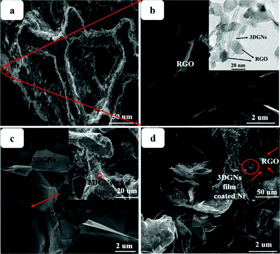
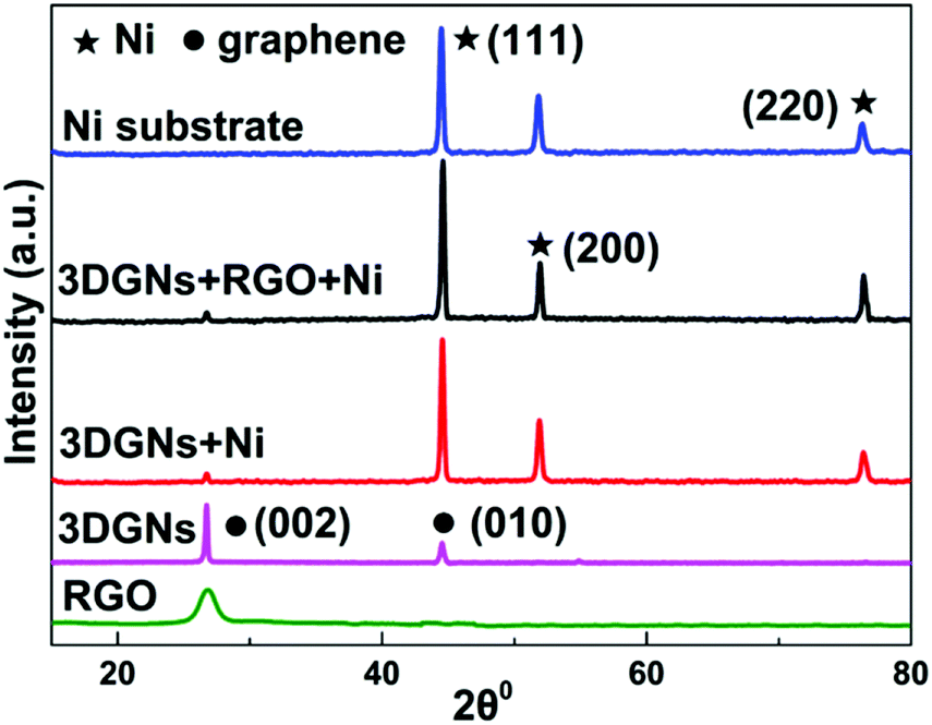
SEM images of various CEs are shown in Fig. 1. The morphology of the RGO-coated Ni substrate prepared using the LBL assembly method is shown in Fig. 1a, and RGO sheets were observed on the surface. The high-magnification image corresponding to the red circle in Fig. 1a is displayed in Fig. 1b. The morphology of the 3DGN-coated Ni electrode is shown in Fig. 1c, and the 3DGN film was identified as the corrupted part at the grain boundary of the Ni substrate due to their different thermal expansion coefficients. The Ni served as the electron collector, while the 3DGNs was expected to provide a perfect highway for electron transport, which was shown to be the case in our previous reports.19,20 The appearance of the RGO–3DGN-based electrode was similar to that of the 3DGN CE, but also showed some extra tablet-shaped objects on the surface (Fig. 1d), which were the loaded RGO nanosheets. The specific fields of these images are marked by the red circles in their insets (Fig. 1c and d). The TEM image acquired of the mixture of RGO and 3DGNs (with Ni substrate removed using hydrochloric acid) is shown in the inset of Fig. 1b. Here, the RGO was observed to be loaded on the surface of the 3DGNs, in line with the SEM images. XRD curves of the pristine Ni substrate, RGO, 3DGNs the resulting CEs are shown in Fig. 2. Diffraction peaks belonging to the (111), (200) and (220) crystal planes of the Ni substrate were observed at 44.5°, 51.6° and 76.3° (JCPDS card: 04-0850), while the signals characteristic of the (002) and (010) crystal planes of the graphene specimens were seen at 26.6° and 44.5° from the 3DGNs (JCPDS card: 41-1487),21 indicating good long-range order of the sample. On the contrary, no (010) diffraction peak of the employed RGO was observed, demonstrating its relatively high defect density and poor continuity due to the harsh conditions of the oxidation–reduction processes. As for the graphene-modified CEs, the signals derived from the 3DGNs and RGO were quite a bit weaker than that of the Ni substrate, attributed to their low mass fractions, in line with the previous report.22
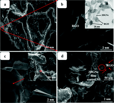 |
| | Fig. 1 SEM images of the (a and b) RGO- (c) 3DGN- and (d) RGO–3DGN-based CEs. The insets display TEM images of the RGO–3DGNs and low-magnification views, and the positions of the high-magnification images are marked in red circles. | |
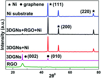 |
| | Fig. 2 XRD patterns of the Ni substrate, RGO, 3DGN, 3DGN-modified CEs, and 3DGN–RGO-co-modified CE. | |
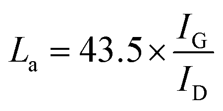
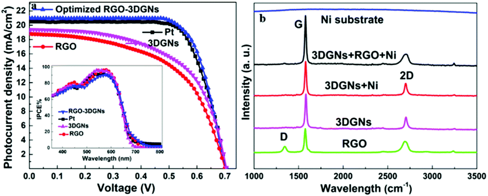
J–V curves of the DSSCs based on these as-prepared CEs are displayed in Fig. 3a. Inspection of these data revealed, for the device using the RGO–3DGN-based CE, a short-circuit current (Jsc) of 20.6 mA cm−2, comparable to that from using a Pt CE and ∼8% higher than those of other graphene-based devices. The open-circuit voltage (Voc) values of all the devices, however, were all similar (∼700 mV). Yet the fill factor (FF) of the DSSCs including the RGO–3DGN CE was also ∼10% higher than those of the other graphene-modified devices (Table 1), indicating the lower resistance resulting from using the RGO–3DGN CE. Considering the otherwise identical conditions (same photoanode, electrolyte and adsorbability for dye molecules), the above-mentioned disparities must have resulted from the different CEs tested. The IPCE curves of the various CE-based devices, shown in the inset of Fig. 3a, were found to be similar, confirming the identical performances of the used photoanodes.15 Raman curves of these CEs were recorded (Fig. 3b) to obtain information on the microstructures of the graphene samples used. Only a broad swell was observed for the Ni substrate, with this result due to its Raman-inactive nature. Therefore, the Raman curves of the as-prepared CEs were similar to those of the original graphene samples. The integrated intensities of the three fingerprint signals, namely the G, D and 2D peaks, were closely related to the morphology and quality of the used RGO and 3DGNs. Specifically, the intensity of the G band was closely related to the thickness of the sample, while the intensity of the D band was highly dependent on its defect density.29 The average size (nm) of the graphene sample can be determined from the integrated intensity ratio IG/ID according to the equation30,31
| |
 | (1) |
 |
| | Fig. 3 (a) J–V curves of DSSCs made using various CEs. The IPCE curves are shown in the inset. (b) Raman curves of the RGO, 3DGNs and the as-prepared CE. | |
Table 1 Photovoltaic performances of the DSSCs made using various CEs. The performances of previously reported DSSCs based on graphene CE are listed for comparison. All of the measurements were recorded under AM-1.5G one sun and the active areas are ca. 0.15 cm2 for all of the cells
| Parameters |
Jsc (mA cm−2) |
Voc (mV) |
FF (%) |
η (%) |
| Pt |
20.5 ± 0.1 |
704 ± 2 |
66.3 ± 0.2 |
9.56 ± 0.11 |
| RGO |
18.8 ± 0.2 |
699 ± 2 |
59.2 ± 0.2 |
7.78 ± 0.23 |
| 3DGNs |
19.4 ± 0.1 |
706 ± 3 |
58.9 ± 0.2 |
8.06 ± 0.12 |
| RGO–3DGNs |
20.6 ± 01 |
701 ± 2 |
65.2 ± 0.2 |
9.42 ± 0.10 |
| Optimized RGO–3DGNs |
21.0 ± 0.2 |
705 ± 2 |
66.1 ± 0.2 |
9.79 ± 0.11 |
| Graphene nanoplatelets17 |
17.20 |
683 |
57.0 |
6.72 |
| Functionalised graphene23 |
13.16 |
640 |
60.0 |
5.00 |
| Ru–GO24 |
16.13 |
770 |
67.0 |
8.30 |
| CoS2–RGO25 |
16.35 |
700 |
67.0 |
7.70 |
| PVP–RGO26 |
14.80 |
860 |
70.0 |
8.90 |
| Co3O4–RGO27 |
15.70 |
760 |
67.7 |
8.10 |
| NiCo2S4–RGO28 |
16.40 |
750 |
66.1 |
8.10 |
Defect density can be roughly defined as (1/La)2 in cm−2.30–32 The results we calculated were based on the IG/ID ratios from various profiles, and are listed in the Table 2. For the 3DGNs, the D peak almost disappeared, indicative of low defect density and good continuity, which would favor the formations of channels enabling fast transport of electrons. But this tendency was apparently counteracted by the poor levels of interface contacts between the graphene basal plane and electrolyte, leading to a photovoltaic performance similar to that resulting from using the RGO CE (Fig. 3).
Table 2 Calculated defect densities of the used graphene samples
| Samples |
Parameters |
| ID/IG |
Defect density (cm−2) |
| RGO |
0.335 |
5.93 × 10⁹ |
| 3DGNs |
0.05 |
1.32 × 10⁸ |
The surface functional groups of the RGO have been indicated to act as a bridge to create a close contact between the graphene basal plane and electrolyte, although these functional groups have also been shown to degrade the intrinsic electrical properties of graphene.5,14,15 Recently, our group found that the surface defects of the 3DGNs can play a similar role and endow the material with a wettability at its interface better than those of other materials such as 3DGNs–TiO2 photocatalysts and 3DGNs–epoxy resin composite thermal interface materials.19,33,34 However, a complex process is needed to control the defect density of the resulting 3DGNs.29 In contrast, the degree of reduction and types of functional groups on the RGO surface are easy to control, e.g., by adjusting the progressions of the oxidation and reduction. Naturally, realizing the functions of the 3DGNs and RGO at the same time in a well-designed CE would be meaningful. In other words, the presence of the RGO was anticipated to improve the electron transport ability at the interface between the graphene basal plane and electrolyte, while the 3DGNs were shown to act as an electron highway promoting the I3−/I redox reaction. The mechanism probably involved the functional groups of the RGO and defects of the 3DGNs acting as the active sites to adsorb the iodide ions and promote the triiodide reduction reaction because of the lowered adsorption energy and the reduced redox potential barrier. Meanwhile, the continuous construct of the 3DGNs formed a highway for fast electron transport and provided abundant electrons to promote the I3−/I redox reaction through the close contact at the interface area with the functional groups of the RGO. Moreover, the good interface condition between the Ni and 3DGNs was also advantageous for the electron transport.35,36 As expected, the combination of the RGO and 3DGNs brought about a remarkable enhancement of the performance of the resulting DSSCs (Table 1, a η as high as 9.42% was achieved), implying the achieved synergy of the 3DGNs and RGO.
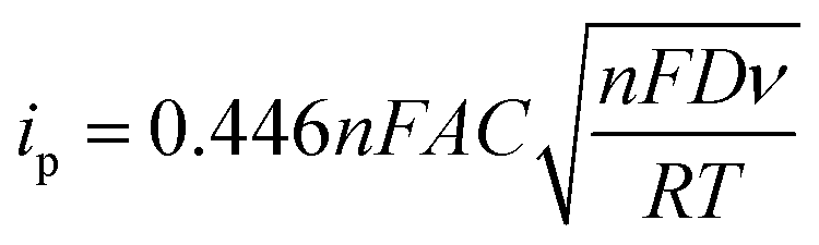
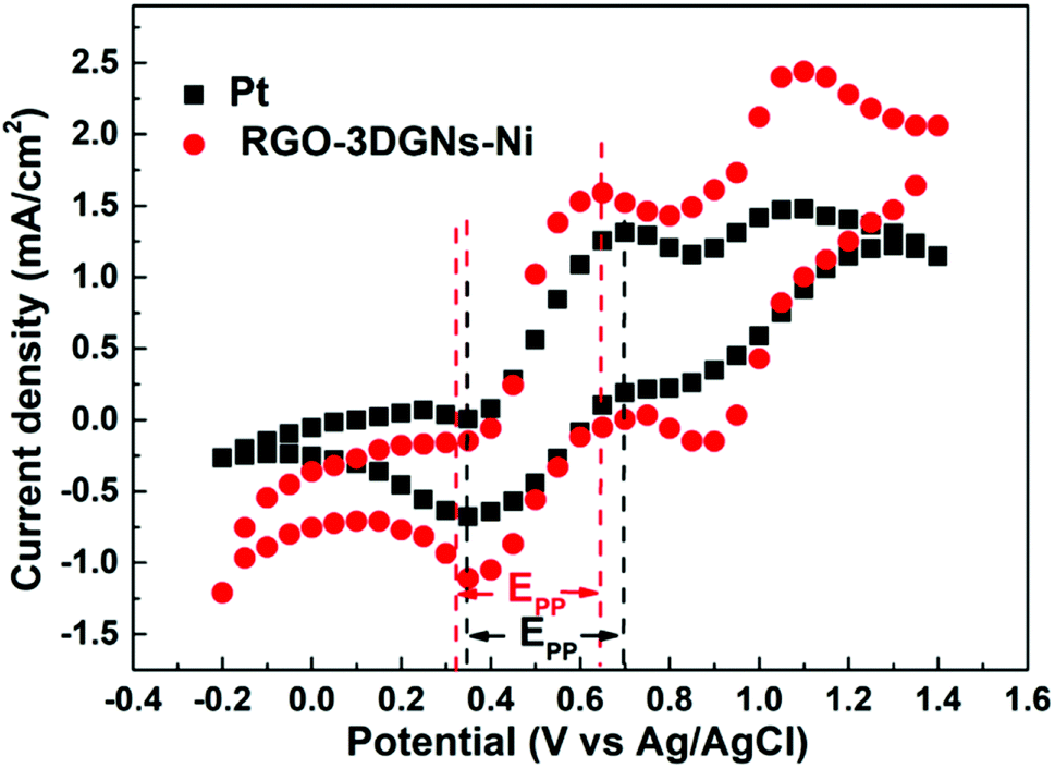
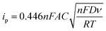
Cyclic voltammetry is widely used to analyze the electrocatalytic activities of CEs.37–39 As shown in Fig. 4, two pairs of redox signals were observed for both the Pt- and the 3DGN–RGO-based CEs. The two peaks located at relatively negative potentials (described as Red1 and Ox1) were assigned to the reduction of I3−, while the more positive peaks were generated by the oxidation of the I2. Considering that the main function of the CE was to reduce the I3− to I−, the values of the Red1 and Ox1 promoted the electrocatalytic performance of the CE. Cathodic current density (Jred1) and peak-to-peak potential separation (Epp, potential difference between the Red1 and Ox1) have been shown to be the determinants of the resulting electrocatalytic behaviors of various CEs. A higher Jred1 demonstrates a faster reduction, while a lower Epp indicates a better reversibility of the redox reaction (which inversely correlates with the electrochemical rate constant). Based on the resulting profiles, the Epp value of the 3DGN–RGO-based CE was slightly less than that of the Pt CE, while the Jred1 of the 3DGN–RGO-based CE was greater than that of the Pt CE, manifesting the high electrocatalytic activity and fast redox kinetics of the former (specific values are listed in the Table 3). The lower Epp was induced by the sufficient available sites for the redox reaction from the defects and functional groups of the RGO,40 while the high Jred1 resulted from the ability of the 3DGNs to rapidly collect and transport electrons. Therefore, the synergy between the 3DGNs and RGO achieved the improved electrocatalytic performances. Furthermore, the relationship between the scan rate, peak current density and diffusion of iodide ions can be calculated based on the Randles–Sevcik equation41
| |
 | (2) |
In this equation,
A,
C,
n,
D,
F,
T and
ν represent electrode area (cm
−2), I
3 concentration (mol cm
−2), number of electrons, diffusion coefficient (cm
2 s
−1), Faraday constant, temperature and scan rate (V s
−1), respectively. The comparable peak currents of the 3DGN–RGO CE and Pt CE indicated their similar diffusion coefficients, confirming the good catalytic activity of the 3DGNs–RGO CE for reducing the I
3− species. Therefore, the combination of the 3DGNs and RGO in the CE not only boosted the electron transport at the interface area, but also promoted the transport of iodide ions. Moreover, the stability performances of the RGO–3DGNs–Ni CE with scan rates of 50 mV s
−1 and 100 mV s
−1 were recorded. Constant peak current densities were observed after 50 cycles, and the specific values are listed in the
Table 4. The degradations of the
Jred1,
Jox1,
Jred2 and
Jox2 were less than 7%, confirming the high stability of the RGO–3DGN–Ni-based CE in the iodide-based electrolyte system.
 |
| | Fig. 4 Cyclic voltammetry curves of various devices. | |
Table 3 The data abstracted from the CV and EIS curves
| CEs |
Jred1 (mA cm−1) |
Epp (mV) |
Rs (Ω cm2) |
RCt (Ω cm2) |
| Pt |
−0.774 |
357.5 |
18.71 |
9.44 |
| RGO–3DGNs–Ni |
−1.112 |
320.8 |
18.90 |
9.61 |
Table 4 The stability of the RGO–3DGN–Ni CE with 50 mV s−1 and 100 mV s−1 scan rates
| Scan rates (mV s−1) |
Parameters |
| Jred1 (mA cm−1) |
Jox1 (mA cm−1) |
Jred2 (mA cm−1) |
Jox2 (mA cm−1) |
| 50 (first time) |
−1.112 |
1.59 |
−0.148 |
2.44 |
| 50 (50 cycles) |
−1.045 |
1.49 |
−0.139 |
2.29 |
| 100 (first time) |
−1.118 |
1.60 |
−0.151 |
2.44 |
| 100 (50 cycles) |
−1.056 |
1.49 |
−0.140 |
2.27 |
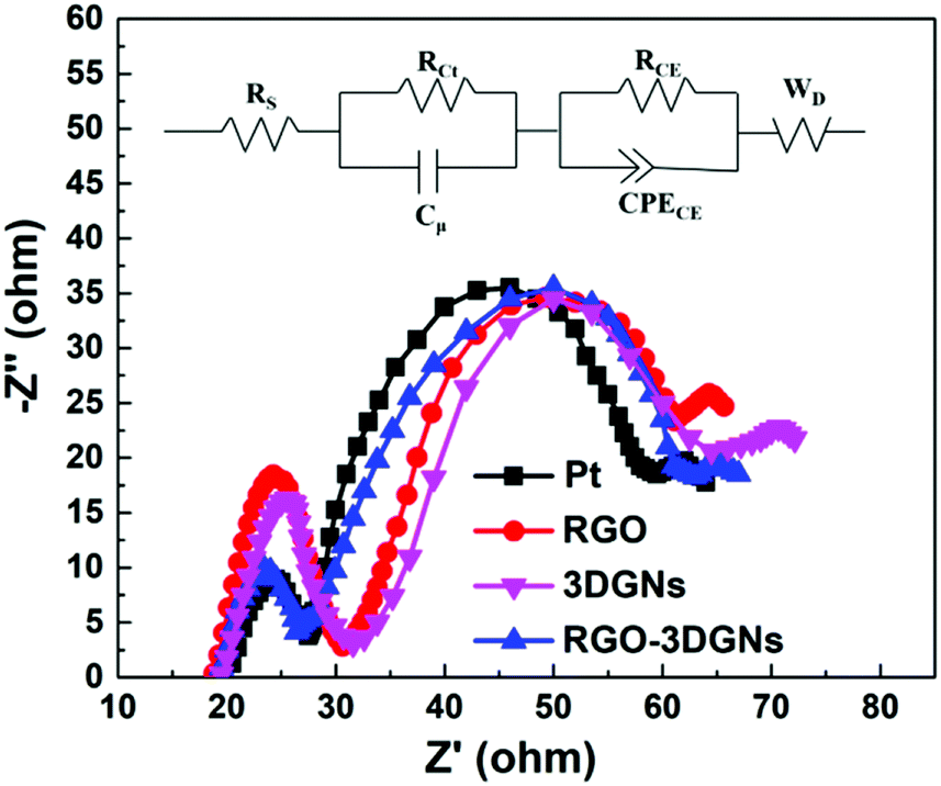
In order to confirm this point, the EIS profiles of various CE-assisted devices were recorded. Two semicircles located at high-frequency and middle-frequency regions were observed in all of the curves (Fig. 5). Similar intensities and diameters of the semicircles in the middle-frequency area indicated that the charge transfer impedance in the photoanode was almost the same, attributed to the identical RGO–TiO2 photoanode having been used.34 In contrast, marked differences were observed for the corresponding signals in the high-frequency area, indicating the significant differences in the charge transport impedance at the CE–electrolyte interface. The EIS results confirmed that the RGO and 3DGNs acted synergistically in the CE, and the electron impedances of the 3DGN–RGO CE and Pt CE were comparable. The equivalent circuit model is displayed in the inset of Fig. 5, and the specific values of the Rs and RCt from the Pt- and RGO–3DGN–Ni-based devices are listed in Table 3. Therein, the Rs was induced by the conductive substrate and CE, while the resistances RCE and CPECE were generated by impedance at the photoanode–electrolyte interface. In general, resistance RCt in parallel with the capacitance Cμ is associated with the impedance at the interface between the CE and electrolyte (with RCt representing the charge-transfer resistance and Cμ the chemical capacitance at the interface), and the Warburg diffusion impedance (WD) is related to the ion diffusion of the electrolyte in DSSCs. The RCt values of the devices based on the RGO–3DGN CE and Pt CE were derived from the equivalent circuit model and found to be comparable, with values, respectively, of 9.61 Ω and 9.44 Ω, indicative of good levels of contact between the RGO–3DGN CE and electrolyte.
 |
| | Fig. 5 EIS profiles of various devices. The equivalent circuit model is displayed as an inset. | |
The relative amount of the RGO included was optimized to further enhance the performance of the resulting CE. The photovoltaic performance improved as the amount of RGO was increased up to about 6%, but then remained about the same with further increases in the amount of RGO. These results were easily explained by a low relative amount of the RGO not having been able to provide sufficient linkers to connect the graphene basal plane and electrolyte, and excess RGO not having further increased the level of interface contact due to the scale of the interface field having been limited and the total photocurrent having been restricted by the intensity of the illumination. The wettability levels of the graphene basal plane and other materials (including inorganic and organic matters) have, according to our recent study, been shown to be also determined by the types of the surface functional groups of the RGO.19,33,34 By adjusting the oxidation and reduction processes, control of the identities and total amounts of surface functional groups can be achieved (as described in relatively high detail in our previous report).42 After optimizing the mass fraction (6%) and reduction degree (Celement/Cfunctional = 2.1:1, Celement:Chydroxyl:Cepoxy:Ccarboxyl = 68:22:2:8) of the employed RGO, a η as high as 9.79% was obtained, comparable with 9.56% value for the device using a Pt electrode and higher than the values previously reported for DSSCs based on graphene CE (the specific photovoltaic performance measures are listed in Table 1 for comparison).23–28,43,44 The detailed C1s XPS curves of the original graphene oxide (GO) and resulting RGO specimens are shown in Fig. 6. The signals located at 284.7 and 288.7 eV were attributed to the sp2-bonded carbon atoms and carbon atoms from the HC–C![[double bond, length as m-dash]](https://www.rsc.org/images/entities/char_e001.gif) O, respectively.45 And the two weaker signals at 287.4 eV and 285.9 eV were ascribed to the CO and C–OH.42 According to the integral intensities of these peaks, the relative amount of elemental carbon increased from 42% for the GO to 68% for the optimized RGO (and the relative amounts of the carbon atoms from various chemical states were abstracted). The sample with a high relative quantity of hydroxyl groups displayed a better performance, implying that this functional group improved the interface contact level between the graphene basal plane and electrolyte, and promoted the I3−/I− redox reaction. Even with all of the above-described advances, there remains a large upside potential for the 3DGN–RGO-based CE because its performance was still limited in the current study by the added adhesive, and thus further optimizations in this regard are underway.
O, respectively.45 And the two weaker signals at 287.4 eV and 285.9 eV were ascribed to the CO and C–OH.42 According to the integral intensities of these peaks, the relative amount of elemental carbon increased from 42% for the GO to 68% for the optimized RGO (and the relative amounts of the carbon atoms from various chemical states were abstracted). The sample with a high relative quantity of hydroxyl groups displayed a better performance, implying that this functional group improved the interface contact level between the graphene basal plane and electrolyte, and promoted the I3−/I− redox reaction. Even with all of the above-described advances, there remains a large upside potential for the 3DGN–RGO-based CE because its performance was still limited in the current study by the added adhesive, and thus further optimizations in this regard are underway.
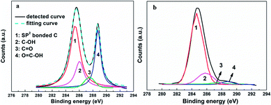 |
| | Fig. 6 XPS curves of the (a) original GO and (b) well-designed RGO samples. | |
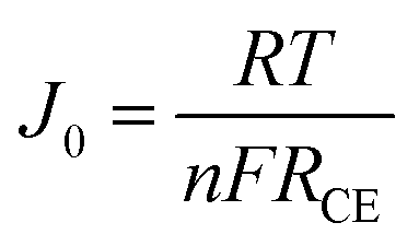
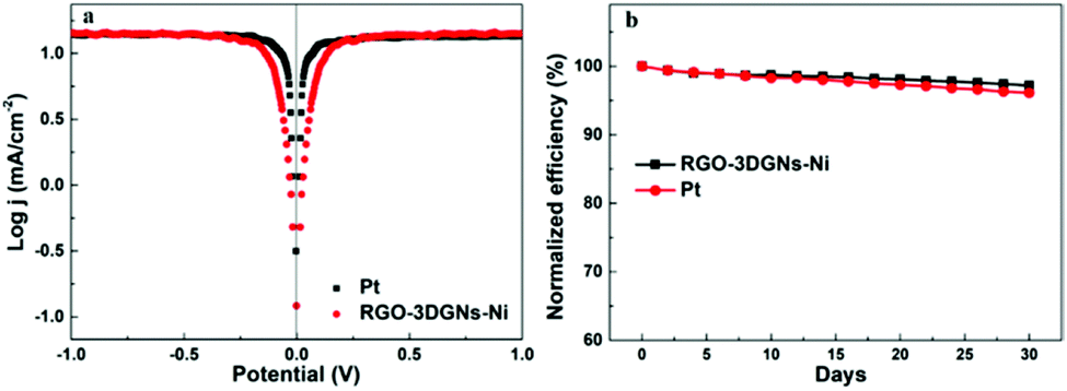
In order to further evaluate the charge transfer performances of the 3DGN–RGO-based CE at the interface with the I3−/I− redox couple, a Tafel polarization curve was recorded with a symmetric cell configuration, and the corresponding profile of the Pt CE was also recorded for comparison (Fig. 7a). In the Tafel field (at medium overpotential with a sharp slope), the exchange current density was derived from the intersection of the cathodic branch when the over-potential was zero. J0 is in general closely related to RCE, and the specific relationship is expressed by the equation46
| |
 | (3) |
where
J0,
R,
T,
F,
n and
RCE represent the exchange current density, molar gas constant, absolute temperature, Faraday constant, number of electrons, and charge-transfer resistance, respectively.
J0 of the 3DGN–RGO-based CE was in this way calculated to be slightly higher than that of the Pt CE, indicating the lower
RCE (which was to a good extent in line with the EIS results) and confirming the good electrocatalytic activity of 3DGN–RGO-based CE, comparable to that of the Pt CE.
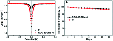 |
| | Fig. 7 (a) Tafel profiles of the DSSC based on the RGO–3DGN CE and that based on the Pt CE. (b) Stability of the RGO–3DGN-CE-based DSSCs. | |
The long-term stability of the 3DGN–RGO CE-based DSSC was tested, and Fig. 7b shows the changes of the efficiency over the course of 30 days. After a month, the efficiency of this DSSC retained 97.2% of its initial value, a bit better than the 96.1% of the initial value retained by the DSSC using a Pt CE, and indicating the high stability of the 3DGN–RGO-based CE in the electrolyte.
Experimental
Materials
Chloroplatinic acid, hydrochloric acid, indoline, protonic polyethyleneimine (PEI) aqueous solution, iodine and potassium iodide were obtained commercially from Aladdin Co. Natural graphite power, phosphorus pentoxide, hydrogen peroxide, polytetrafluoroethylene (adhesive), sodium dodecyl sulfate (SDS) and sulfuric acid were purchased from a Shanghai chemical reagent plant. Deionized water was used to prepare all aqueous solutions.
Preparation
The preparation of the 3DGNs and RGO has been reported in our previous reports.33,47,48 The RGO- and 3DGN-based CEs were fabricated as follows. For RGO CE, the Ni substrate was immersed alternately into an aqueous solution of PEI (10 min) and an RGO solution (15 min), and these two steps were repeated 100 times to prepare the RGO electrode. (The PEI was then removed from the electrode by irradiating it with UV light for 6 h.) The 3DGN CE was prepared using the CVD method, with foam Ni used as the template.22 As for the RGO–3DGN CE, specified quantities of RGO sheets (with mass fractions ranging from 1–10 wt%) were each loaded using an adhesive onto the surface of a 3DGN CE (with mass fraction of the 3DGN set at 4 wt% by controlling the CVD reaction time). The photoanode was prepared as follows. RGO (2 wt%) was manually stirred together with a TiO2 solution, and then the resulting mixture was combined with ethanol under an ultrasonic processing (30 min). Afterward, the obtained paste was moved to a conductive glass by applying a doctor-blade approach. The thicknesses of the resulting CEs and photoanodes were 40 μm and 15 μm. The preparation of the resulting DSSCs have been described in the previous reports.4,5,47 Briefly, the prepared photoanodes were immersed into 0.5 mmol of an indoline dye solution with a 1:1 (volume) mixture of acetonitrile and butanol and kept in that state for 30 h. The photoanode and CE were assembled into sandwich-type cells and fixed using a crocodile clip. An electrolyte consisting of an acetonitrile solution, 0.5 mol LiI and 0.05 mol I2 was injected into the space between the electrodes. In order to confirm the reproducibility of the obtained high performance levels, each kind of CE was prepared four times, and the resulting properties of each device were abstracted based each on the average of three repeats of the measurement.
Characterizations
Morphology images were recorded using a scanning electron microscope (SEM, FEI Sirion 200 scanning electron microscope). Raman spectra were recorded using a LabRam-1B Raman microspectrometer at 514.5 nm (Horiba Jobin Yvon, France). X-ray diffraction (XRD) patterns were acquired using a Bruker D8 Advance (Cu Kα radiation 0.154 nm). X-ray photoelectron spectroscopy (XPS) profiles were measured on an RBD upgraded PHI– 5000C ESCA system (PerkinElmer). Photovoltaic measurements were taken on a CHI 660D electrochemical analyser (Shanghai CH Instrument Company, China). J–V curves were recorded using a PGSTAT 30 potentiostat (Netherlands). The IPCE profiles were recorded on a Newport 1918-c power meter. Cyclic voltammogram, Tafel polarization and electron impedance spectroscopy data were collected by using an Autolab (PGSTAT302N electrochemical workstation system, Metrohm). The cyclic voltammograms were acquired with a regular three-electrode system where Ag/AgCl and Pt were adopted as the references, and the scan rates were 50 mV s−1 and 100 mV s−1.
Conclusions
RGO–3DGN-based CEs were prepared to replace the Pt CE and to endow the resulting DSSCs with high photovoltaic performance. Here, the 3DGNs provided a network amenable to fast transport of electrons, the RGO acted as a bridge to achieve the close contact between the graphene basal plane and electrolyte, and synergy between the 3DGNs and RGO accelerated the I3−/I− the redox reaction. The mass fraction of the RGO was found to be a vital factor influencing the resulting properties, and the obtained performances were also highly dependent on the total amount and types of its surface functional groups. Optimizing the 3DGN–RGO CE yielded a η as high as 9.79%, comparable to that using a Pt electrode, and revealing the potential prospects of the 3DGN–RGO CE in the DSSC field of study.
Conflicts of interest
There are no conflicts to declare.
Acknowledgements
This work is supported by National Natural Science Foundation of China (No. 51506012, 51574044, 51706023), Natural Science Foundation of Jiangsu Province (No. BK20150266).
Notes and references
- L. C. Chen, C. H. Hsu, P. S. Chan, X. Y. Zhang and C. J. Huang, Nanoscale Res. Lett., 2014, 9, 380–386 CrossRef PubMed
 .
. - Z. K. Yue, G. Z. Wu and X. Chen, Mater. Lett., 2017, 192, 84–87 CrossRef CAS .
- Y. E. Shin, Y. J. Sa and S. Park, Nanoscale, 2014, 6, 9734–9741 RSC .
- B. Tang, G. J. Ji, Z. W. Wang, H. Q. Chen, X. F. Li, H. G. Yu, S. Li and H. Liu, RSC Adv., 2017, 7, 45280–45286 RSC .
- B. Tang, H. G. Yu, H. P. Peng, Z. W. Wang, S. Li, T. T. Ma and W. Q. Huang, RSC Adv., 2018, 8, 29220–29227 RSC .
- D. Tasis, Catalysts, 2017, 7, 234–252 CrossRef .
- M. X. Wu, X. Lin, Y. D. Wang, L. Wang, W. Guo, D. D. Qi, X. J. Peng, A. Hagfeldt, M. Grätzel and T. L. Ma, J. Am. Chem. Soc., 2012, 134, 3419–3428 CrossRef CAS PubMed .
- M. Chen, L. L. Shao, Y. X. Guo and X. Q. Cao, Chem. Eng. J., 2016, 304, 303–312 CrossRef CAS .
- M. Chen, L. L. Shao, Z. Y. Yuan, Q. S. Jing, K. J. Huang, Z. Y. Huang, X. H. Zhao and G. D. Zou, ACS Appl. Mater. Interfaces, 2017, 9, 17949–17960 CrossRef CAS .
- M. Chen, G. C. Wang, L. L. Shao, Z. Y. Yuan, X. Qian, Q. S. Jing, Z. Y. Huang, D. L. Xu and S. X. Yang, ACS Appl. Mater. Interfaces, 2018, 10, 31208–31224 CrossRef CAS .
- C. Chen, M. C. Long, C. H. Zhang and W. M. Cai, Nanoscale Res. Lett., 2012, 7, 101–105 CrossRef .
- M. Jie, S. Wei, L. Cheng, Z. Jie and Y. Fei, J. Chem. Eng., 2017, 319, 155–162 CrossRef .
- M. Jie, L. Cheng, Y. Fei and J. H. Chen, ChemSusChem, 2014, 7, 3304–3311 CrossRef PubMed .
- H. J. Ahn, I. H. Kim, J. C. Yoon, S. I. Kima and J. H. Jang, Chem. Commun., 2014, 50, 2412–2415 RSC .
- B. Tang and G. X. Hu, J. Power Sources, 2012, 220, 95–102 CrossRef CAS .
- W. Yang, X. W. Xu, Y. L. Gao, Z. Li, C. Y. Li, W. P. Wang, Y. Chen, G. Q. Ning, L. Q. Zhang, F. Yang, S. L. Chen, A. J. Wang, J. Kong and Y. F. Li, Nanoscale, 2016, 8, 13059–13066 RSC .
- S. S. Nemala, K. S. Aneja, P. Bhargava, H. L. M. Bohm, S. Mallick and B. Sivasambu, Electrochim. Acta, 2018, 285, 86–93 CrossRef CAS .
- M. Chen and L. L. Shao, Chem. Eng. J., 2016, 304, 629–645 CrossRef CAS .
- B. Tang, H. Q. Chen, Y. F. He and Z. W. Wang, Compos. Sci. Technol., 2017, 150, 54–64 CrossRef CAS .
- Y. F. Hung, C. Cheng, C. K. Huang and C. R. Yang, Nanomaterials, 2019, 9, 376–390 CrossRef PubMed .
- B. Tang and G. X. Hu, Chem. Vap. Deposition, 2014, 20, 14–22 CrossRef CAS .
- B. Tang, H. Q. Chen, H. P. Peng, Z. W. Wang and W. Q. Huang, Nanomaterials, 2018, 8, 105–131 CrossRef PubMed .
- J. D. R. Mayhew, D. J. Bozym, C. Punckt and I. A. Aksay, ACS Nano, 2010, 4, 6203–6211 CrossRef PubMed .
- V. D. Dao, L. L. Larina, J. K. Lee, K. D. Jung, B. T. Huy and H. S. Choi, Carbon, 2015, 81, 710–719 CrossRef CAS .
- H. Yuan, J. Liu, Q. Jiao, Y. Li, X. Liu, D. Shi, Q. Wu, Y. Zhao and H. Li, Carbon, 2017, 119, 225–234 CrossRef CAS .
- Y. C. Liu, P. Zhai, M. N. Lu, C. C. Lee, K. S. K. Reddy, Y. Tingare, C. Y. Yeh and T. C. Wei, Energy Technol., 2017, 5, 756–764 CrossRef CAS .
- T. Jiang, S. Yang, P. Dai, X. Yu, Z. Bai, M. Wu, G. Li and C. Tu, Electrochim. Acta, 2018, 261, 143–150 CrossRef CAS .
- K. S. Anuratha, M. Ramaprakash, S. K. Panda and S. S. Mohan, Ceram. Int., 2017, 43, 10174–10182 CrossRef CAS .
- B. Tang, P. F. Zhou and D. W. Wu, J. Changzhou Univ., Nat. Sci. Ed., 2017, 29, 48–54 Search PubMed .
- N. Salisu, Z. H. Mohd, A. Y. Nor and Z. Zulkarnain, Nanomaterials, 2017, 7, 182–199 CrossRef PubMed .
- B. Tang, G. X. Hu and H. Y. Gao, Int. J. Heat Mass Transfer, 2015, 85, 420–429 CrossRef CAS .
- B. Tang, X. F. Li, W. Q. Huang, H. G. Yu and X. Ling, Nanoscale Res. Lett., 2018, 13, 276–283 CrossRef PubMed .
- B. Tang, H. Q. Chen, Y. F. Sun, M. G. Lin, Z. W. Wang, H. G. Yu, T. T. Ma and S. Li, RSC Adv., 2018, 8, 27811–27817 RSC .
- B. Tang, S. L. Wang, J. Zhang, Z. W. Wang, Y. F. He and W. Q. Huang, Int. Mater. Rev., 2018, 63, 204–225 CrossRef CAS .
- M. Chen, G. Zhao, L. L. Shao, Z. Y. Yuan, Q. S. Jing, K. J. Huang, Z. Y. Huang, X. H. Zhao and G. D. Zou, Chem. Mater., 2017, 29, 9680–9694 CrossRef CAS .
- S. C. Hou, X. Cai, H. W. Wu, X. Yu, M. Peng, K. Yan and D. H. Zou, Energy Environ. Sci., 2013, 6, 3356–3362 RSC .
- Q. G. He, Y. L. Tian, J. J. Wu, J. Liu, G. L. Li, P. H. Deng and D. C. Chen, Nanomaterials, 2019, 9, 429–444 CrossRef PubMed .
- S. M. Mohamed, M. Moaaed and A. M. B. Nasser, Catalysts, 2019, 9, 139–148 CrossRef .
- H. T. Chih, H. F. Po, M. L. Chia and L. S. Shiao, Coatings, 2018, 8, 21–33 CrossRef .
- S. N. Siva, S. A. Karanveer, B. Parag, B. H. L. Mallika, M. Sudhanshu and B. Sivasambu, Electrochim. Acta, 2018, 285, 86–93 CrossRef .
- H. Y. Yuan, W. F. Chi, W. C. Huang, W. S. Wang, C. J. Shih and C. H. Tsai, Org. Electron., 2016, 31, 207–216 CrossRef .
- Y. F. Sun, Y. F. He, B. Tang, C. B. Tao, J. M. Ban and L. Jiang, RSC Adv., 2017, 7, 55790–55795 RSC .
- J. Ma, W. Shen and F. Yu, J. Power Sources, 2017, 351, 58–66 CrossRef CAS .
- B. Tang, G. X. Hu, H. Y. Gao and Z. X. Shi, J. Power Sources, 2013, 234, 60–68 CrossRef CAS .
- Y. F. Sun, B. Tang, W. Q. Huang, S. L. Wang and Z. W. Wang, Appl. Therm. Eng., 2016, 103, 892–900 CrossRef CAS .
- B. L. Pang, S. Lin, Y. T. Shi, Y. Y. Wang, Y. J. Chen, S. Ma, J. G. Feng, C. K. Zhang, L. Y. Yu and L. F. Dong, Electrochim. Acta, 2019, 297, 70–76 CrossRef CAS .
- Y. F. Sun, Y. H. Cao, W. Q. Huang and B. Tang, Mater. Lett., 2016, 165, 178–180 CrossRef CAS .
- B. Tang, Z. W. Wang, W. Q. Huang, S. Li, T. T. Ma, H. G. Yu and X. F. Li, Nanoscale Res. Lett., 2017, 12, 527–533 CrossRef PubMed .
|
| This journal is © The Royal Society of Chemistry 2019 |
Click here to see how this site uses Cookies. View our privacy policy here. 
 Open Access Article
 This Open Access Article is licensed under a Creative Commons Attribution-Non Commercial 3.0 Unported Licence
 a,
Haogang Yua,
Weiqiu Huang
a,
Haogang Yua,
Weiqiu Huang