
 Open Access Article
 This Open Access Article is licensed under a Creative Commons Attribution-Non Commercial 3.0 Unported Licence
The effect of excess selenium on the opto-electronic properties of Cu2ZnSnSe4 prepared from Cu–Sn alloy precursors†
Teoman Taskesen *,
Devendra Pareek,
Janet Neerken,
Johannes Schoneberg,
Hippolyte Hirwa,
David Nowak,
Jürgen Parisi and
Levent Gütay
*,
Devendra Pareek,
Janet Neerken,
Johannes Schoneberg,
Hippolyte Hirwa,
David Nowak,
Jürgen Parisi and
Levent Gütay
Laboratory for Chalcogenide-Photovoltaics (LCP), Energy and Semiconductor Research Laboratory (EHF), Institute of Physics, Carl von Ossietzky University of Oldenburg, Carl-von-Ossietzky-Straße 9-11, D-26111 Oldenburg, Germany. E-mail: teoman.taskesen@uni-oldenburg.de
First published on 3rd July 2019
Abstract
For the fabrication of a kesterite-type CZTSe absorber material, stacked elemental-alloy layers (SEAL) precursor consisting of Cu–Sn alloy and elemental Zn layers offer the possibility of enhanced process control due to their advantages such as improvement of material homogeneity and suppression of the commonly observed Sn loss. In this study, the impact of selenium amounts during the annealing of a SEAL-type precursor with the configuration of Zn/Cu–Sn/Zn was demonstrated. The obtained results demonstrate how the selenium amount can indirectly be used to influence the absorber composition in the described annealing process and its direct impact on the opto-electronic properties of solar cells. This occurs due to the placement of elemental Sn in the vicinity of the sample during annealing that acts as a further source of SnSe2 vapor during the high-temperature stage of the process depending on the degree of selenium excess. The results show that higher selenium amount increases the band gap of kesterite; this is directly accompanied by a shift of the defect activation energies. Optimization of this effect can lead to widening of the space-charge width up to 400 nm, which improves the charge carrier collection. The described optimization strategy leads to device efficiencies above 11%.
Introduction
Cu2ZnSn(S,Se)4 is one of the promising absorber materials that can be used in a single-junction solar cell or as a part of a tandem device structure in the thin film photovoltaic industry in the future. This quaternary material has attracted attention due to its environmentally friendly constituent elements and the steady development of solar cell performance, reaching device efficiencies above 12%.1,2In recent years, scientific studies have shown that there are several challenges regarding this material that can be considered as critical pre-requisites before reaching its industrial relevance. The most dominant obstacle that is currently being discussed is the open-circuit voltage deficit Voc-def caused by the existence of a large number of defects in the absorber itself.3 This mainly results in the formation of band tails in the material and non-radiative recombination through deeper defect states within the band gap.4
Moreover, one of the reasons for the existence of these defects is the quaternary structure of kesterite. The presence of 4–5 elements in the crystal lattice can cause numerous possible types of anti-site and vacancy defects. Some of these or their combinations, referred to as defect clusters, have been reported to have an impact on the band gap, doping, and non-radiative recombination in kesterite absorbers.5 In addition, Cu and Zn are chemically similar elements and can easily switch positions in the lattice; this creates unavoidable defect formations, often referred to as the Cu–Zn disorder. Recently, a significant effort has been reported to overcome this obstacle by adding a larger atom, such as silver, cadmium, or barium, into the crystal lattice for exchanging the concerned elements.6 This approach has been shown to be useful to improve the device properties by reducing the band tails; however, it has not solved the general problem of Voc-def.
The preferential formation of specific defects in the absorber is often related to its composition. This can be illustrated in the pseudo-ternary phase diagram, where different regions in the diagram indicate the preferential formation of specific defects and clusters. In addition to the final absorber composition in the diagram, the route through the diagram during processing can be expected to affect the type of defects and clusters formed. In particular, the formation of Sn(S,Se)2–x during the synthesis of kesterite can be quite harmful to the device performance. Sn(S,Se)2–x can easily escape from the absorber at high synthesis temperatures due to its high volatility, causing a change in the absorber composition and defect landscape. This effect is usually referred to as “Sn loss” in kesterite. The accompanying possible formation of Sn-related deep defects within the band gap of the absorber would cause significant bulk recombination. Moreover, one of the approaches proposed to prevent this Sn loss is the use of precursors in which Sn is mainly embedded in the Cu–Sn alloy configuration, which in combination with a properly designed selenization procedure can suppress the formation of volatile Sn(S,Se)2−x; this would ultimately help to maintain a constant Sn amount throughout the annealing process.7,8 An appropriate configuration of alloy precursors during kesterite processing is also known to improve the thin film homogeneity;9,10 moreover, using this alloy structure, reproducible and resilient kesterite absorber processing with device efficiencies above 11% can be achieved.11,12
In this study, we report the optimization of the selenium amount during the annealing process for precursor stacks with Cu–Sn alloy layers. We have discussed the crucial impact of excess Se on the material properties and fine-tuning of the Se amount for improving the opto-electronic properties of the Cu2ZnSnSe4 (CZTSe) material that finally results in the enhanced performance of solar cell devices.
Experimental
The CZTSe absorbers were fabricated by a sequential growth process: the deposition of precursors and subsequent annealing under a chalcogen atmosphere. The precursor layer stacking order was Mo/Zn/Cu–Sn/Zn, with the total layer thickness of 850 nm (Mo = 550 nm and Zn/Cu–Sn/Zn = 300 nm). To study the impact of selenium, the amount of selenium in the semi-closed graphite susceptor was varied between 20 mg and 210 mg. Moreover, 10 cm of an elemental Sn wire was placed in the graphite susceptor in all the cases. A single-step annealing process was performed in a conventional tube furnace at the heating rate of 10 °C min−1 followed by 20 minutes of dwelling at 530 °C. The samples were naturally cooled down after the process. The prepared CZTSe absorber layers were further processed to solar cells. The final device structure was Mo/CZTSe/CdS/i-ZnO/Al:ZnO. The detailed processing parameters can be found in the literature.11,12The absorbers and the final devices were then characterized in terms of their material properties and device performances by the usual methods including current–voltage (IV), external quantum efficiency (EQE), capacitance–voltage (CV), energy-dispersive X-ray spectroscopy (EDX), scanning electron microscopy (SEM), Raman spectroscopy, and photoluminescence (PL) measurements as described in previous studies.11,12
For thermal admittance spectroscopy (TAS) measurements, the devices were mounted in a cold finger closed-cycle cryostat at a pressure below 10−4 mbar. Prior to the measurements, the sample was left at room temperature and in the dark for 2 hours to reach a relaxation state. For the measurements, the devices were first cooled at 50 K, and the temperature was then ramped from 50 K to 330 K in steps of 10 K. The temperature of the devices was monitored by a Pt-100 sensor mounted on top of the devices. Using the Solartron SI-1260 impedance gain/phase analyzer, the admittance was measured at zero bias with the excitation frequency of Vac = 30 mV for the frequencies ranging from 10 Hz to 1 MHz. A parallel equivalent circuit model was used to separate the conductance and the capacitance.
Results and discussion
To understand the influence of selenium amount on the overall composition of the absorber, EDX measurements were performed on bare absorbers, which were selenized using selenium in different amounts. Fig. 1 depicts the atomic ratios of Cu/Zn, Cu/Sn, and Zn/Sn as a function of the amount of selenium; two main features are observed in this graph. The first feature is related to the Zn content. As can be seen in Fig. 1, the Cu/Zn ratio does not change for the samples with the Se amount in the range of 80–210 mg. Speculating that the amount of Cu is stable during the annealing process, a constant Cu/Zn ratio suggests that the selenium amount does not have any direct influence on the resulting content of Zn, which is a volatile species in its elemental form. However, when selenium is present in low amounts (i.e., between 20 mg and 50 mg, marked by a circle in Fig. 1), upon decreasing the amount of selenium, the Cu/Zn ratio decreases, and the Zn/Sn ratio increases. These trends indicate higher Zn content in the samples selenized with low selenium amounts. For further understanding, Raman measurements were performed for the sample selenized using 20 mg of selenium (Fig. 2). The Raman spectrum obtained using a green laser (532 nm) shows sharp Raman peaks at 196 cm−1 and 174 cm−1, confirming the presence of the kesterite CZTSe phase as the main phase with no clear indications of secondary phases even at this low amount of Se. However, the Raman spectrum obtained under excitation by a blue laser (457.9 nm) shows a clear peak at 250 cm−1, revealing that there is a non-negligible portion of the ZnSe phase on the absorber surface that is not present for higher Se amounts. This suggests that the kesterite formation reaction is only partially completed at this low selenium amount. This phase segregation of ZnSe on the absorber surface (also indicated by bright spots adjacent to the large grains in the SEM image in Fig. 2) explains the enhanced Zn detection during the EDX measurements for the samples grown in this low selenium regime.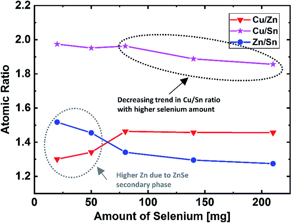 | ||
| Fig. 1 Atomic ratios of Cu/Zn, Cu/Sn, and Zn/Sn as a function of the selenium amount used during the selenization process. | ||
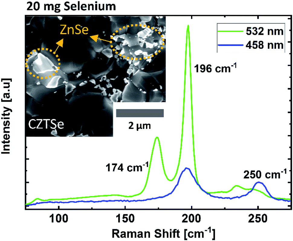 | ||
| Fig. 2 SEM images and Raman spectra obtained using green and blue lasers for the CZTSe absorber selenized with 20 mg of selenium. | ||
The second feature observed in Fig. 1 is the decreasing trend of the Cu/Sn ratio with the increasing selenium amount. To confirm that this change corresponds to the composition of the kesterite phase itself (and not to the segregated secondary phases), the intensity ratios of the main kesterite Raman bands I1 (196 cm−1) and I2 (174 cm−1) have been determined. In literature, this ratio has been reported to correlate with the Cu/(Zn + Sn) ratio in the kesterite phase, and the decreasing [I2]/[I1] ratio can be attributed to a compositional change towards lower Cu/(Zn + Sn) ratio (relatively Cu-poor kesterite).13 Fig. 3(a) and (b) display the behavior of the [I2]/[I1] Raman band ratios, which show a decreasing trend with the increasing selenium amounts; this indicates a compositional shift towards lower Cu/(Zn + Sn) ratio. These results are consistent with the observed trend in the EDX measurements. As discussed earlier, the Cu and Zn contents can be considered to be constant for high Se amounts, i.e. ≥80 mg. Thus, it can be concluded that the trend of the Cu/Sn ratio and accordingly that of the Cu/(Zn + Sn) ratio must result mainly from a varied Sn content. This is further supported by the similar trend observed for the Zn/Sn ratio for the higher Se amount of ≥80 mg.
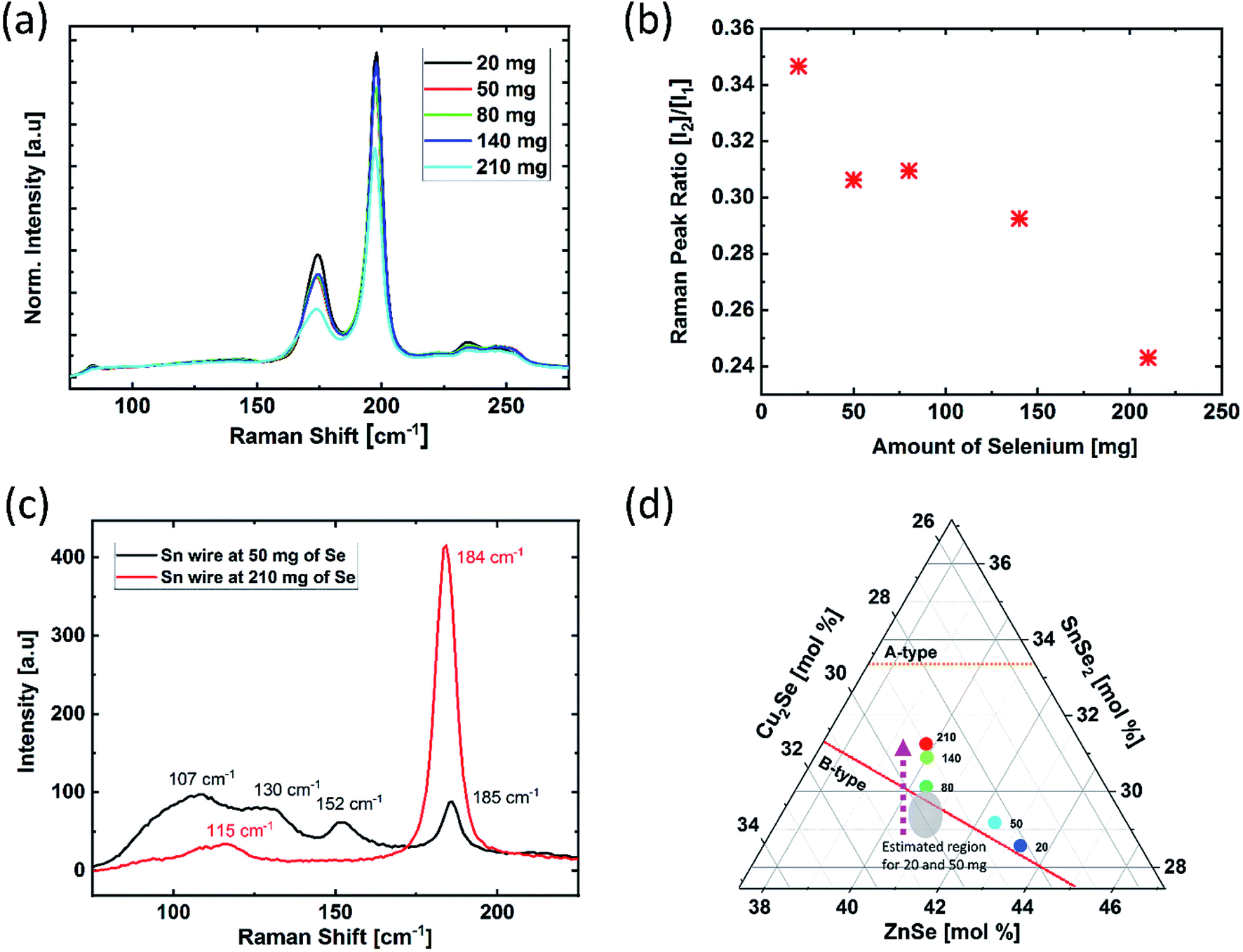 | ||
| Fig. 3 (a) Raman spectra of the absorbers synthesized with various selenium amounts. (b) Raman [I2]/[I1] band intensity ratio as a function of selenium amount. A lower [I2]/[I1] ratio indicates a decrease in the Cu/(Zn + Sn) ratio. (c) The Raman spectra of the elemental Sn-wire after reaction at 400 °C with two different selenium amounts. (d) The compositional pseudo-ternary phase diagram demonstrating the shift from the B-type towards the A-type zone with the varying selenium amount. The estimated regions of 20 mg and 50 mg samples without the influence of secondary phases during the EDX measurements are marked by a grey circle. | ||
The change in the Sn content can be explained by the combination of two possible reasons. The first reason is related to the incomplete formation reaction due to the limited amount of selenium. As abovementioned, we used a Cu–Sn alloy layer in the precursor stack. During selenization, once Se starts to evaporate, its vapor reaches the precursor layer and reacts with the available structure of the precursor. At this point, most of Sn in the precursor layer is bound in the Cu–Sn alloy, and effectively, no elemental Sn is available. Hence, the kesterite formation reaction takes place with the suppressed formation of SnSe2−x (which is prone to evaporation), and the Sn loss is directly prevented, which we have described in detail elsewhere;7,8 however, at extremely low selenium amounts, the overall selenization reaction slows down due to insufficient vapor pressure of selenium; this leaves more time for the metallic precursor stack to undergo the re-alloying reactions that can ultimately lead to the Cu–Sn alloy disintegration and formation of elemental Sn.7,8 In this case, the SnSe2−x phases can start to form and escape from the absorber layer; this leads to a net loss in the Sn amount at the end of the annealing process. However, the first reason can only explain the higher Cu/Sn ratio in the absorber selenized with selenium at a very low amount (i.e. <80 mg).
For all the cases where the selenium vapor pressure is higher than that required for the completion of the kesterite formation reaction (i.e. selenium amount ≥80 mg), selenization would tend to start from a stable alloy configuration in the precursor (i.e. without alloy disintegration), which suppresses the formation of SnSe2−x and prevents Sn loss; this would result in a stable Sn content.7 Based on this understanding, we can explain the second reason as follows: with excess amounts of selenium, the trend of increasing Sn content and decreasing Cu/Sn ratio can be explained by the incorporation of additional Sn at higher temperatures (T > 500 °C) during the annealing process. As abovementioned in the experimental section, in addition to the elemental Se pellets, we placed an elemental Sn-wire inside the graphite susceptor. This elemental Sn acts as an additional source of the SnSe2−x vapor during the high-temperature stage of the annealing process.7,8 As the effect of the Se amount on this mechanism of additional Sn incorporation was not previously investigated, we performed two annealing experiments in which we interrupted the selenization process at 400 °C and performed a Raman analysis on the initial elemental Sn-wire used in the susceptor. Fig. 3(c) illustrates the Raman spectra of the elemental Sn-wires after reaction using 50 mg and 210 mg of selenium. The results show that in the case of a lower selenium amount (50 mg), elemental Sn has reacted mostly to form the SnSe phase, whereas in the case of a high selenium amount (210 mg), we mainly observed SnSe2; as reported in the literature, SnSe2 has a significantly higher vapor pressure than SnSe, which then leads to enhanced Sn incorporation into the absorber due to higher Se amounts in the susceptor. Hence, this mechanism explains the general trend of the decreasing Cu/Sn ratio for higher selenium amounts.
By combining these two mechanisms, enhanced Sn content is observed after the annealing processes with higher selenium amounts. This means that the absorbers become more Cu-deficient, as also observed from the Raman peak ratios; this shifts the material composition from the range of the B-type line towards the range of the A-type line with the increasing selenium amount (shown in Fig. 3(d)).14 This compositional shift may also lead to a change in the predominantly expected defect clusters from [2ZnCu + ZnSn] to [ZnCu + VCu]. The consequences of this possible change of the predominant defect clusters have been discussed later in more detail.
Herein, note that the selenium amount also induces some morphological changes in the absorber film. A higher amount of selenium leads to a larger CZTSe grain size and lateral homogeneity in the absorber film, similar to other studies reported in the literature.15 These changes can be explained by a more homogenous distribution of the composition, particularly that of the Cu2−xSe phase, along the sample during the growth of kesterite in the case of higher selenium amounts. More details are presented in the ESI.†
After the compositional and structural analysis, all the absorbers were processed to solar cells. The device parameters obtained via the IV measurements are presented in Fig. 4. The presented set of results clearly shows the impact of selenium amount on the achieved device performance of the solar cells. At first, the solar cells prepared with 20 mg Se showed poor device performance, which could be expected due to the incomplete formation reaction and the presence of ZnSe phases on the absorber surface, as explained earlier. Furthermore, it can be seen that the device performance increases for higher amounts of Se up to 210 mg and then starts to decrease. An additional data point of 280 mg selenium was added to observe the trend beyond the main sample series. The results indicate the optimum amount of Se in our process configuration to be at around 210 mg, at which the power conversion efficiency exceeds 11%. The device properties of the main sample series were then examined in detail to further understand the reason behind efficiency improvement.
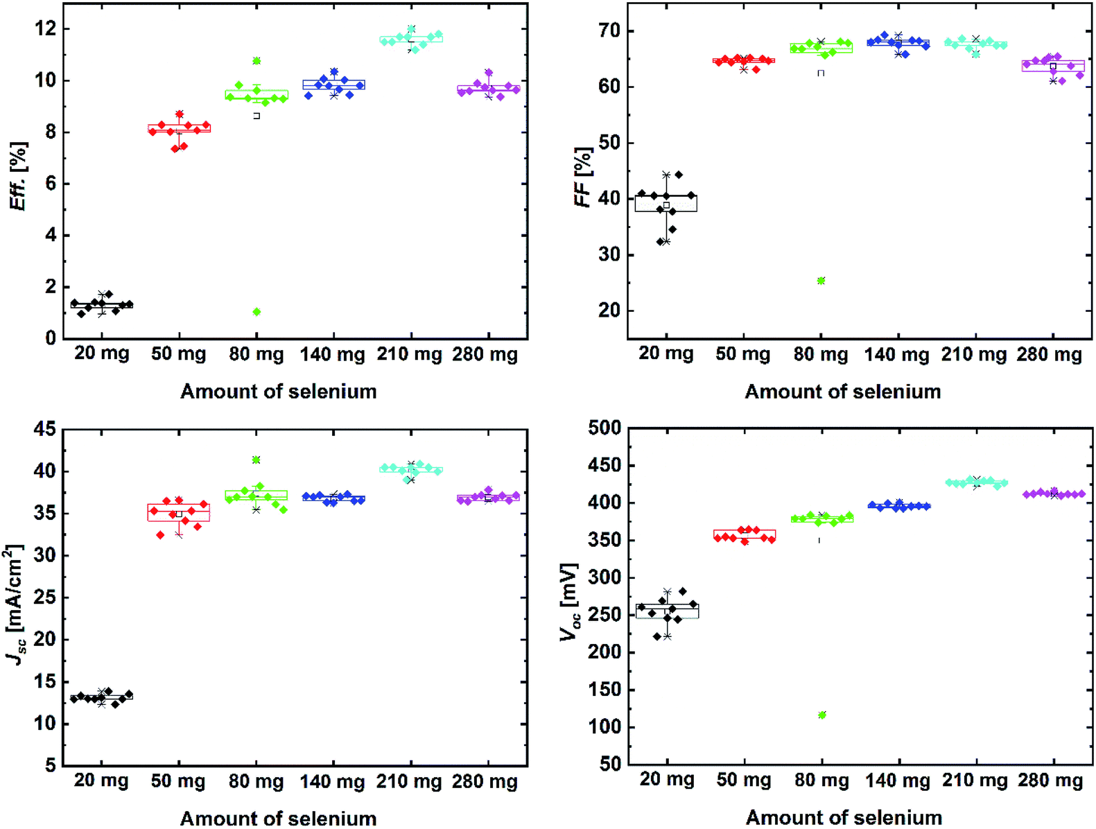 | ||
| Fig. 4 Device parameters obtained from the I–V measurements using a calibrated solar simulator under the standard test conditions. Each sample contains 9 devices with the device area of ∼0.22 cm2 each. An additional data point with 280 mg of selenium was added to observe the following trend. | ||
The most apparent change observed from the device parameters is for Voc, which shows a clear increase with the increasing Se amount, with the maximum amount of 210 mg. In literature, it is reported that an increase in the selenium vapor pressure reduces the band tails in the band structure of kesterite; this leads to improvements in the open-circuit voltage.16 To observe whether Voc improved regardless of the band gap variations, the Voc-def values were determined according to the Shockley–Queisser limit, as presented in Table 1. The comparison of data shows that the obtained Voc-def values of the devices does not change with the selenium amount but rather remain at the same level. The fill factors of the investigated devices seem to be only slightly influenced by the changes in the Se amount. The trend of the fill factor could also be correlated to its dependence on Voc. These findings point out that the improvement of device efficiency with the increasing selenium amount must be related to current enhancement in the device.
| Amount of Se [mg] | Voc-def [V] | Eg [eV] | EPL [eV] | Eg − EPL [eV] |
|---|---|---|---|---|
| 50 | 0.35 | 0.95 | 0.95 | 0.00 |
| 80 | 0.34 | 0.97 | 0.96 | 0.01 |
| 140 | 0.35 | 1.00 | 1.00 | 0.00 |
| 210 | 0.34 | 1.02 | 1.02 | 0.00 |
| 280 | 0.37 | 1.03 | 1.03 | 0.00 |
To investigate the current collection behavior in the devices, we performed EQE measurements for all the samples. Fig. 5(a) depicts the EQE spectra of the devices. At 20 mg Se, the solar cell exhibits a low overall EQE and severe losses at long wavelengths, which can be attributed to significant collection losses induced by the recombination and transport barriers. This behavior is in agreement with the poor device performance. Starting from 50 mg, one noticeable change is an increasing trend of the band gap towards higher selenium amounts. The band gap of the absorber (obtained by fitting of EQE2 vs. energy) increased from 0.95 eV up to 1.03 eV with the increasing selenium amount (Table 1). The increase in the band gap with the increasing selenium amount can be attributed to the change in the predominantly expected defect clusters from [2ZnCu + ZnSn] to [ZnCu + VCu] due to the compositional shift, as abovementioned, since these defect clusters have been reported to cause different band edge energies in kesterite.5 For a deeper investigation of the band gap shift and its possible impact on radiative recombination, we performed PL spectroscopy for all the samples. The normalized PL spectra are depicted in Fig. 5(b). Herein, two major changes are observed in the data. The first change that is visible in the PL spectrum is for annealing with 20 mg selenium. It can be clearly seen that in addition to the main PL peak at 0.95 eV, the 20 mg selenium sample contains additional PL emissions at higher energies. In literature, these emissions have been reported to indicate the ZnSe secondary phase.17 With an increase in the selenium amount to 50 mg, the intensity of this contribution is significantly reduced and disappears for 80 mg of selenium; this is in agreement with the abovementioned Raman and EDX data. The second major change observed is the blue-shift of the main PL peak with the increasing amount of selenium. The main PL peak energy for the lowest amount of selenium (20 mg) is 0.95 eV and increases up to 1.03 eV for 280 mg of selenium, which follows the same trend as observed for the band gap obtained from EQE (Table 1). In addition to this, the difference between the PL peak energy and band gap (determined by the EQE-spectrum) is equal to 0 and does not change with the amount of selenium (Table 1). This means that the main PL emission originates from the band-to-band transition for all the samples regardless of the selenium amount. Furthermore, we can conclude that there is no indication that the amount of Se can have any significant impact on band tail related radiative recombination below the band gap in the present study.
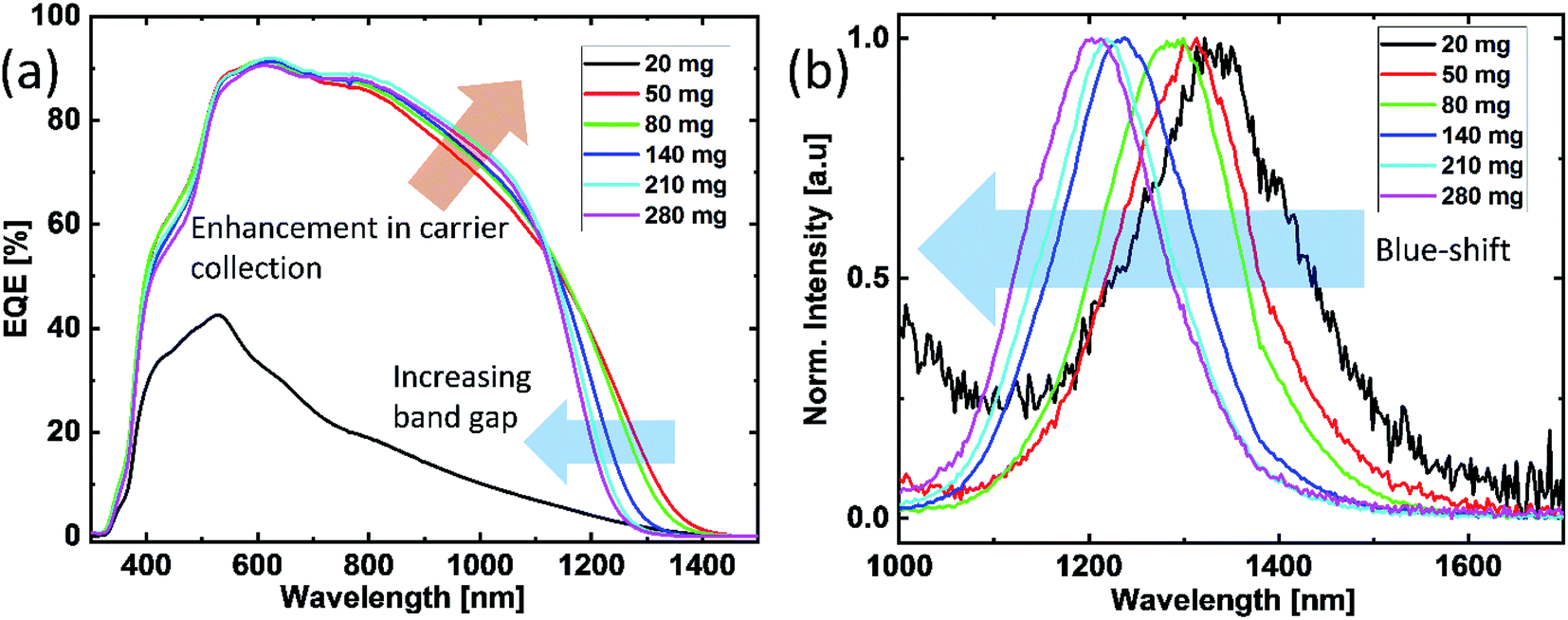 | ||
| Fig. 5 (a) EQE spectra of the devices. Higher selenium amount increases the band gap and current collection at longer wavelengths. (b) Photoluminescence spectra of the solar cells, obtained at room temperature. | ||
In addition to these effects of the band gap increase, the EQE spectra (Fig. 5(a)) in the range of 800–1100 nm indicate an enhanced charge carrier collection for the samples with higher selenium amounts. This could result from an increased space-charge width or minority carrier diffusion length. The space-charge widths of the devices are derived from the C–V measurements, as presented in Fig. 6. The device with 50 mg selenium displays a space-charge width of about 150 nm. With increasing amount of selenium, the space-charge width also increases and reaches a value of about 400 nm, which appears to be rather high when compared to those in the literature.18 This remarkable increase can explain the enhancement in the current collection at longer wavelengths, which is visible in EQE. Even though a noticeable decrease in the current is expected due to a higher band gap, the increase in the space-charge width actually over-compensates the effect expected from the increased band gap and leads to an overall improvement of the device performance. It is worth mentioning that the enhancement in current collection is more pronounced in the I–V measurement than that seen in the EQE spectrum. This slight difference in Jsc and EQE can be related to the photo-doping of the layers, which then behave slightly different under the light bias, as reported in literature.19 More information related to this context can be found in the ESI.†
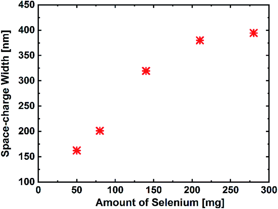 | ||
| Fig. 6 The average space-charge width from 9 devices for each selenium amount, obtained by capacitance–voltage measurements. | ||
To investigate the influence of different degrees of selenium excess on the resulting defect landscape in the material, the activation energies were determined from the TAS measurements by following the procedure developed by T. Walter (Fig. 7(a)).20 The results show that the activation energy for lowest selenium amount (50 mg) is 85 meV, increasing to 200 meV for the highest Se-containing sample. Considering the fact that the band gap also increases with the increasing selenium amount, these activation energies are most likely related to the same defect state that stays on the same energy level relative to the vacuum level, whereas the band edges shift away. This conclusion is additionally confirmed by the Meyer–Neldel rule. As shown in Fig. 7(b), a Meyer–Neldel type relationship between the thermal pre-factor and the activation energy is found as expected for processes originating from the same thermally activated process.21,22 This means that this defect level is not linked to the band edge like it is in the case for many shallow defects. We attribute this defect to the CuZn anti-site, which has the activation energy of 110 meV (±50 meV). In literature, both the theoretical and the experimental studies have reported that this defect is considered to be the dominantly occurring defect in CZTSe, independent of the absorber composition.23 These results suggest that when the band gap of kesterite increases with the increasing selenium amount, the band edge energy of the valence band shifts down, increasing its energetic distance from the acceptor defect position (in other words, the valence band position moves further away from the acceptor defect state), i.e. increases activation energy for this defect state. As a consequence, a decrease in the free carrier concentration at room temperature is expected due to less ionization of this defect. To confirm this, we have determined the effective carrier concentration from the CV measurements, which reflects the net doping at room temperature, as presented in Fig. 8. The results show that the carrier concentration decreases from 2.3 × 10¹⁶ to 5.0 × 10¹⁵ with the increasing selenium amount, as expected from the increased activation energy. This finding can also explain the trend observed for the space-charge width, where low free carrier concentration results in a wider space-charge region. As a consequence, the charge carrier collection is improved, leading to higher device efficiencies.
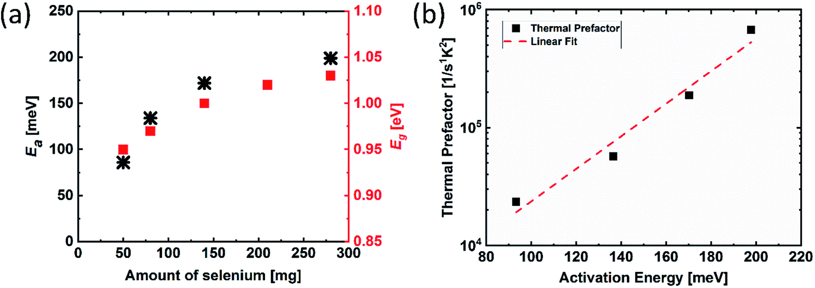 | ||
| Fig. 7 (a) Activation energy determined from TAS as a function of selenium amount. (b) The relation between thermal pre-factor and activation energy. The defect activation energy is determined by following the procedure developed by T. Walter. | ||
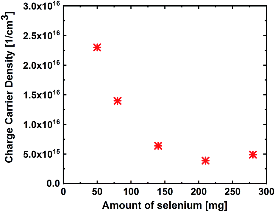 | ||
| Fig. 8 Effective carrier concentration determined from the capacitance–voltage measurements on the solar cells. | ||
Conclusion
In this study, we focused on the optimization of the selenization procedure in a sequential growth process. We have presented the importance of selenium excess during the annealing process and its influence on the absorber properties, in the case of a SEAL-type precursor containing a Cu–Sn alloy layer, and additional elemental Sn placed in the susceptor during annealing. The findings demonstrate that an increase in selenium amount results in enhanced incorporation of Sn into the absorber via SnSe2 vapor pressure created by the additional Sn source. A compositional shift of kesterite from the B-type zone towards the more A-type zone due to Sn incorporation was observed, which possibly changed the predominantly expected defect clusters from [2ZnCu + ZnSn] to [ZnCu + VCu], increasing the band gap of kesterite from 0.95 eV to 1.03 eV. As a consequence of the band gap increase, the valence band edge moved further away from the acceptor defect state; this decreased the effective carrier concentration at room temperature. Lower free-carrier concentration resulted in a wider space charge width, extending up to 400 nm, with the increasing selenium amount, which ultimately increased the charge carrier collection. Thus, due to the combined enhancement of Voc and Jsc, the device performance increased above 11% with the increasing selenium amount.The present study also partially shows the impact of using an additional Sn source during the selenization process at high temperatures and demonstrates the indirect control of this Sn source by adjusting the Se excess in the reaction volume. The addition of Sn into the susceptor can be used as a tool to tune the material composition and properties, opening up a new optimization parameter.8 It is finally essential to note that the changes occurring in the absorber with chalcogen are not only important during the fabrication of the kesterite film, but can also be significant for the post-treatment steps; at post-treatment temperatures above 220 °C, selenium depletion can start to occur in the absorbers, and also, the possible changes in the predominant defect clusters, band gap, and composition have to be taken into account. The approach and findings presented in this study appear to be of a general nature for CZTSe processing and can therefore also be used as a template for optimizing the selenization processes of other configurations.
Conflicts of interest
There are no conflicts to declare.Acknowledgements
The authors gratefully acknowledge the funding received from the German Ministry of Education and Science (BMBF), Grant No. 03SF0530A (“Free-Inca”). The authors thank Dr Erik Ahlswede and co-workers (ZSW Stuttgart) for kindly providing the Mo-substrates. The authors further thank Vincent Steininger and Timo Pfeiffelmann for their contributions to this work.References
- W. Wang, M. T. Winkler, O. Gunawan, T. Gokmen, T. K. Todorov, Y. Zhu and D. B. Mitzi, Adv. Energy Mater., 2014, 4, 1301465 CrossRef.
- S. K. Wallace, D. B. Mitzi and A. Walsh, ACS Energy Lett., 2017, 2, 776–779 CrossRef CAS.
- S. Siebentritt, Nat. Energy, 2017, 2, 840–841 CrossRef.
- G. Rey, G. Larramona, S. Bourdais, C. Choné, B. Delatouche, A. Jacob, G. Dennler and S. Siebentritt, Sol. Energy Mater. Sol. Cells, 2018, 179, 142–151 CrossRef CAS.
- T. Gershon, T. Gokmen, O. Gunawan, R. Haight, S. Guha and B. Shin, MRS Commun., 2014, 4, 159–170 CrossRef CAS.
- J. Li, D. Wang, X. Li, Y. Zeng and Y. Zhang, Adv. Sci., 2018, 5, 1700744 CrossRef PubMed.
- D. Pareek, T. Taskesen, J. M. Prieto, H. Stange, D. Nowak, T. Pfeiffelmann, W. Chen, C. Stroth, M. H. Sayed, U. Mikolajczak, J. Parisi, T. Unold, R. Mainz, and L. Gütay, Presented at 9th European Kesterite Workshop, Ghent, 2018, to be published 2019 Search PubMed.
- T. Taskesen, D. Pareek, D. Nowak, W. Kogler, T. Schnabel, E. Ahlswede and L. Gütay, Z. Naturforsch., 2019 DOI:10.1515/zna-2019-0136.
- M. A. Olgar, J. Klaer, R. Mainz, L. Ozyuzer and T. Unold, Thin Solid Films, 2018, 628, 1–6 CrossRef.
- M. A. Olgar, J. Klaer, R. Mainz, S. Levcenco, J. Just, E. Bacaksiz and T. Unold, Thin Solid Films, 2018, 615, 402–408 CrossRef.
- T. Taskesen, V. Steininger, W. Chen, J. Ohland, U. Mikolajczak, D. Pareek, J. Parisi and L. Gütay, Prog. Photovolt: Res. Appl., 2018, 26, 1003–1006 CrossRef CAS.
- T. Taskesen, J. Neerken, J. Schoneberg, D. Pareek, V. Steininger, J. Parisi and L. Gütay, Adv. Energy Mater., 2018, 8, 1–6 Search PubMed.
- J. Márquez, M. Neuschitzer, M. Dimitrievska, R. Gunder, S. Haass, M. Werner, Y. E. Romanyuk, S. Schorr, N. M. Pearsall and I. Forbes, Sol. Energy Mater. Sol. Cells, 2016, 144, 579–585 CrossRef.
- S. Chen, A. Walsh, X.-G. Gong and S.-H. Wei, Adv. Mater., 2013, 25, 1522–1539 CrossRef CAS PubMed.
- Y. Wei, D. Zhuang, M. Zhao, Q. Gong, R. Sun, L. Zhang, X. Lyu, X. Peng, G. Ren, Y. Wu and J. Wei, J. Alloys Compd., 2018, 755, 224–230 CrossRef CAS.
- B. Shin, Y. Zhu, N. A. Bojarczuk, S. Jay Chey and S. Guha, Appl. Phys. Lett., 2012, 101, 053903 CrossRef.
- Ö. Demircioğlu, J. F. L. Salas, G. Rey, T. Weiss, M. Mousel, A. Redinger, S. Siebentritt, J. Parisi and L. Gütay, Opt. Express, 2017, 25, 5327 CrossRef PubMed.
- Y. S. Lee, T. Gershon, O. Gunawan, T. K. Todorov, T. Gokmen, Y. Virgus and S. Guha, Adv. Energy Mater., 2015, 5, 1401372 CrossRef.
- F. Liu, C. Yan, K. Sun, F. Zhou, X. Hao and M. A. Green, ACS Photonics, 2017, 4, 1684–1690 CrossRef CAS.
- T. Walter, R. Herberholz, C. Müller and H. W. Schock, J. Appl. Phys., 1996, 80, 4411–4420 CrossRef CAS.
- A. Yelon, B. Movaghar and R. S. Crandall, Rep. Prog. Phys., 2006, 69, 1145–1194 CrossRef CAS.
- T. Eisenbarth, T. Unold, R. Caballero, C. A. Kaufmann and H.-W. Schock, J. Appl. Phys., 2010, 107, 034509 CrossRef.
- S. Bourdais, C. Choné, B. Delatouche, A. Jacob, G. Larramona, C. Moisan, A. Lafond, F. Donatini, G. Rey, S. Siebentritt, A. Walsh and G. Dennler, Adv. Energy Mater., 2016, 6, 1502276 CrossRef.
Footnote |
| † Electronic supplementary information (ESI) available. See DOI: 10.1039/c9ra2779c |
| This journal is © The Royal Society of Chemistry 2019 |