DOI:
10.1039/C9RA02601K
(Paper)
RSC Adv., 2019,
9, 18371-18376
Hot electrons generated by intraband and interband transition detected using a plasmonic Cu/TiO2 nanodiode
Received
7th April 2019
, Accepted 3rd June 2019
First published on 11th June 2019
Abstract
The use of metal nanoparticles, including Au, Ag, Cu, and Al, can increase the efficiency of photovoltaic devices by electromagnetic field enhancement, which is driven by the excitation of localized surface plasmon resonance. Direct energy conversion from light into electricity via the decay of surface plasmons causing the excitation of hot electron–hole pairs is also a feasible channel. The generation of hot electrons in metal nanostructures can occur through intraband excitation within the conduction band or through interband transition, which is caused by transitions from other bands to the unoccupied conduction band states. Here, we show the distinction between hot electron generation induced by intraband excitation and interband transition on a plasmonic Cu/TiO2 nanodiode by measuring the current conversion efficiency with a monochromator system. We also show the dependence of the production of photocurrent on the thickness of the Cu layer and the effect of an aluminum oxide protection layer on the hot electron flux versus oxidation of the Cu layer. Our results can provide a better understanding for copper-based hot electron photovoltaics, which could lead to more efficient plasmonic energy conversion.
1. Introduction
Localized surface plasmon resonance (LSPR) can occur via confinement of the collective vibration of free electrons in a metal nanostructure and the electric field of incident light.1,2 Two important effects of LSPR excitation are great enhancement of electric fields near the metal nanoparticle surface and optical absorption by the particle with a maximum at the plasmon resonance frequency.3,4 The most popular plasmonic materials are gold, silver, copper, and aluminium, and the advantages of plasmonic metal structures have been widely used to increase the efficiency of various types of photovoltaics and photocatalysts.5,6 In recent years, however, it has been found that plasmonic nanostructures can directly convert photons into electricity on their own by producing hot electrons.7–10 After light is absorbed into the nanostructure and LSPR appears, the plasmons decay by transferring their energy to the electrons in the metal, resulting in the excitation of highly energetic electrons.11 However, hot electrons are rapidly thermalized with a short lifetime on the order of tens of femtoseconds, and most incident photon energy cannot be harvested. Thus, it is important to extract the hot electrons before they lose this excess energy. There are several proposed structures for using hot electrons, including Schottky or tunnelling barriers that are capable of filtering electrons with high energy.12–15 These novel schemes for solar energy conversion offer many possibilities for realizing ways to exceed the performance of conventional photovoltaics and photocatalytic devices or to completely replace traditional conversion systems.
The generation of hot electrons in metal nanostructures can occur through intraband excitation within the conduction band (from occupied s-band to empty s-band) or through interband transitions, which are caused by transitions from other bands to the unoccupied conduction band states (d-band to empty s-band).1,16 The interband transition energy levels of plasmonic metals are 2.15 eV for Cu, 2.4 eV for Au and 4 eV for Ag.17 Therefore, when silver is illuminated with visible light, hot electrons can only be produced by intraband excitation.18 Gold and copper, on the other hand, are capable of interband excitation in the visible region because it is possible to generate hot electrons with a relatively lower energy than those generated via interband excitation in Ag.19,20 To extract these energetic electrons, n-type semiconductors with a high Fermi level are mainly used as acceptors, such as TiO2, which can form a Schottky barrier with plasmonic metals and has a wide bandgap.21–23 TiO2 is also an excellent electron-accepting material that has a high density of state (DOS) in the conduction band, enabling rapid electron injection. However, not all excited hot electrons are extracted to the TiO2 because of the presence of the Schottky barrier. Thus, with Au/TiO2, the hot electrons generated by the interband transition under visible light have a very low extraction probability because their energy is not sufficient to overcome the Schottky barrier height of around 1 eV created at the interface of the Au/TiO2.24
There are several recent studies where copper is used to replace silver and gold, which are the most widely researched metals in the plasmonic field of study.25–28 As the work function of copper (4.65 eV) is smaller than that of gold (5.1 eV), it can form a Schottky barrier with the TiO2 layer with a lower height. Since the interband transition energy level of copper is also lower than gold, it is possible to produce hot electrons with higher energy. Therefore, it is expected that a Cu/TiO2 structure can detect hot electrons excited from both intraband excitation and interband transition, thereby greatly increasing the extraction efficiency. Furthermore, copper is much less expensive than silver or gold, so the use of copper can develop more cost-effective plasmonic devices. Nevertheless, copper-based plasmonic structures have not been actively studied. In fact, copper is easily oxidized in ambient air and has a major weakness of gradually losing LSPR excitation, which hinders the use of copper to fabricate stable devices. To prevent the oxidation of copper, various studies have been carried out, such as using a capping agent,29,30 deposition of insulating materials on copper,31 and alloying copper with other elements.32
Here, we will verify hot electron detection by measuring the steady-state photocurrent using plasmonic Cu/TiO2 nanodiodes with a randomly connected copper nano-island structure. From the current–voltage curve of the plasmonic Cu/TiO2, information about the electrical characteristics, including the Schottky barrier height, was obtained. Furthermore, we prove LSPR excitation by measuring the incident photon-to-current conversion efficiency (IPCE). To distinguish the extraction of hot electrons by intraband excitation and interband transition, both the absorbance spectrum and IPCE are used. Lastly, we demonstrate a stable Cu/TiO2 photodiode with the deposition of an Al2O3 film that contributes to delaying the degradation of the copper layer.
2. Experimental methods
2.1 Fabrication of Cu/TiO2 nanodiodes
Cu/TiO2 Schottky nanodiodes were fabricated as follows. A 150 nm thick Ti layer was first deposited by an electron beam evaporator on a 500 nm SiO2 wafer, which was wet oxidized on a p-type Si (100) wafer. The Ti deposition was done with a 4 × 7 mm2 mask at 2 × 10⁻⁶ torr with an evaporation rate of 0.5 Å s−1. The Ti film was then heat treated at 500 °C in ambient air for 2 h to make the TiO2 film. Two electrode pads consisting of Ti and Au films were deposited using a 5 × 5 mm2 mask. The Ti and Au films for the electrode pads were 50 and 150 nm thick, respectively, and both were deposited at a rate of 1.0 Å s−1 under 2 × 10⁻⁶ torr. One of the pads is in contact with the TiO2 surface to make an ohmic contact and the other pad is deposited on the SiO2 surface to create a terminal connected with the Schottky contact. To fabricate the Schottky contact, a 5 nm thick plasmonic Cu film was deposited on top of the wafer, crossing the TiO2 and Ti/Au electrode pads using a 2 × 10 mm2 mask. For deposition of the plasmonic Cu layer, the vacuum pressure was 2 × 10⁻⁶ torr and the evaporation rate was 0.2 Å s−1. Lastly, a 10 nm thick Al2O3 protection layer was made at 2 × 10⁻⁶ torr with an evaporation rate of 0.2 Å s−1.
2.2 Characterizations of Cu/TiO2 nanodiodes
The current–voltage (I–V) curves and photocurrents were obtained using a source meter (Keithley Instrumentation 2400) with a 4-point probe station. Incident light was illuminated from a tungsten-halogen lamp (9 mW cm−2) perpendicular to the diode surface. The IPCE was measured at 400–900 nm with a Xe arc lamp source (Newport, TLS-300XU), which was utilized to tune the wavelength. To characterize the absorbance properties of the metal films, thin metal layers were prepared on a transparent quartz substrate and measured with an UV-vis spectrometer (Shimadzu, UV-2600).
3. Results and discussion
3.1 Photoelectrical properties of Cu/TiO2 nanodiode
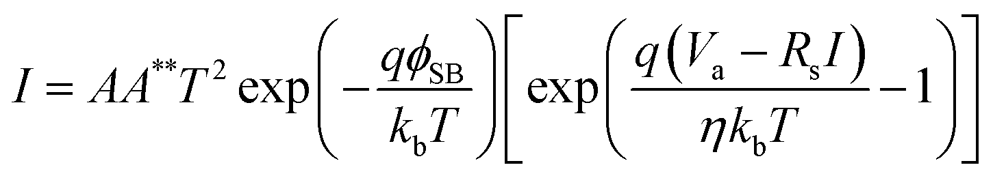
To observe the hot electron flow, a plasmonic Cu/TiO2 nanodiode was fabricated as shown in Fig. 1(a). The nanodiode is composed of two Ti/Au ohmic electrode pads (one at each end), and the active area (Cu/TiO2) is located at the center of the diode. The morphology of the plasmonic Cu film exhibits closely packed and randomly connected Cu nanoclusters. Once hot electrons are generated in the copper film, they travel into the TiO2 layer and make an electrical circuit, which is capable of measuring the steady-state current on the Cu/TiO2 diode. In Fig. 1(b), a short-circuit photocurrent of about 250 nA for the 5 nm Cu film was obtained on the fabricated diode with visible incident light. Since hot electrons generated on the plasmonic Schottky diode can be detected as a current only if they overcome the energy barrier, the height of the Schottky barrier is an important factor determining the photocurrent. Theoretically, we can predict the Schottky barrier height using the Schottky–Mott rule:where ϕSB is the Schottky barrier height, ϕm is the work function of the metal, and χ is the electron affinity of the semiconductor. As the work function of Cu is 4.65 eV, and the electron affinity of TiO2 is 4.0 eV, the Schottky barrier height should be 0.65 eV. To confirm the barrier height of our Cu/TiO2 diode, the I–V curve was measured (Fig. 1(c)). By fitting the results obtained in the I–V curves to the thermionic emission equation, the barrier height can be obtained experimentally. The thermionic emission equation is defined as| |
 | (2) |
where A is the area, A** is the effective Richardson constant, ϕSB is the Schottky barrier height, kb is the Boltzmann constant, T is the temperature, Rs is the series resistance, and η is the ideality factor. Based on eqn (2), the series resistance and ideality factor were determined to be 124.5 Ω and 2.24, respectively. In addition, the Schottky barrier height of Cu/TiO2 was ϕSB = 0.63 ± 0.01 eV, which is comparable with the theoretically predicted value.
 |
| | Fig. 1 (a) Schematic drawing of the plasmonic Cu/TiO2 nanodiode and scanning electron microscope (SEM) image of the plasmonic Cu layer. (b) Steady-state photocurrent measured on the plasmonic Cu/TiO2. (c) Current–voltage curve measured on the plasmonic Cu/TiO2 diode. (Inset) Current–voltage curve and fit of the measured current–voltage data to the thermionic emission equation in log scale. | |
3.2 Hot electron extraction mechanism of Cu/TiO2 nanodiode
To understand the extraction mechanism for hot electron generation on the Cu/TiO2 Schottky nanodiode, the IPCE was measured, which is the current conversion efficiency of hot electrons as a function of incident photon energy (Fig. 2(a)). For comparison, we also probed the nanodiode with Au instead of Cu, which is a widely studied plasmonic metal, but has a higher work function (5.1 eV) and deeper d-band energy level from the Fermi level (2.4 eV) than Cu. In the IPCE of the Au/TiO2 diode, one distinct peak was observed at 600 nm corresponding to LSPR excitation. On the other hand, the Cu/TiO2 diode exhibited clear increases in the IPCE at 450 and 675 nm. These results imply that the Cu/TiO2 diode has two different types of hot electron transfer mechanism. For a more detailed analysis, the absorbance spectrum was measured on both the plasmonic Cu and Au layers. As shown in Fig. 2(b), increased peaks corresponding to the LSPR excitation of Cu and Au were observed at 675 and 600 nm, respectively, which are in accordance with the IPCE results. Furthermore, both materials clearly show an increase in absorbance at wavelengths less than 550 nm for Cu and 480 nm for Au from the interband transition. Note that the increase in absorbance of the Cu and Au means that hot electron production was enhanced. Interestingly, however, in the IPCE of the Au/TiO2 diode, there is a negligible increase in the interband transition region. This is because only a small portion of hot electrons generated by the interband transition in Au could surpass the Schottky barrier height of the Au/TiO2. In contrast to the gold, the Cu/TiO2 diode can convert hot electrons generated by both intra- and interband excitation into photocurrent, enabling efficient detection of the hot electrons. The two types of hot electron transfer processes via intraband excitation and interband transition in Cu/TiO2 are illustrated in the energy band structure (Fig. 2(c)). Since the 3d-band energy level of Cu lies 2.15 eV below the Fermi energy level, at least 2.75 eV of photon energy is required for interband transition hot electrons to be detected as a photocurrent. Meanwhile, the hot electrons excited from the 4s-band have a barrier of around 0.6 eV, so they can be extracted at a relatively lower photon energy. Also, the density of state of the 3d-band is stronger in the narrower energy region, while the 4s-band appears as a weak DOS in the wider energy region. Correspondingly, it is clearly shown in the IPCE of the Cu/TiO2: the sharp IPCE peak at 2.7 eV (460 nm) is higher in the narrower photon energy region than that at 1.9 eV (650 nm).
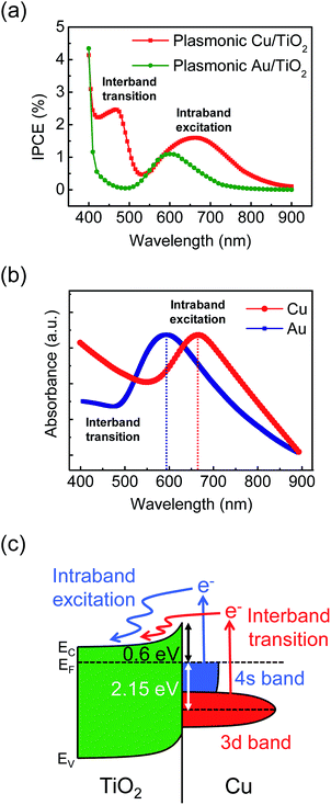 |
| | Fig. 2 (a) IPCE of the plasmonic Cu/TiO2 and Au/TiO2 diodes. (b) Absorbance of the plasmonic Cu and Au. The LSPR peaks at 675 nm for Cu and 600 nm for Au correspond to intraband excitation. The increased absorbance at wavelengths below 550 nm for Cu and 480 nm for Au is attributed to interband transition. (c) Energy band diagram of the Cu/TiO2 structure. Mechanism for hot electron generation from the 4s-band of Cu by intraband excitation and from the 3d-band of Cu by interband transition. | |
3.3 Relationship between hot electron extraction and thickness of Cu film
Fig. 3(a) shows a plot of the photocurrent observed on the Cu/TiO2 diode with Cu film thicknesses of 5–20 nm. The photocurrent of a diode with a thinner Cu layer is higher than that with a thicker Cu film. In general, hot electrons are mainly produced on the metal surfaces that directly absorb light. This means that the bottom of the metal layer, which forms the Schottky interface with the TiO2, is not beneficial for generating hot electrons, while the metal surface is highly beneficial. Furthermore, hot electrons have a short mean free path (∼30 nm for Cu33) because of their rapid cooling dynamics. Therefore, as the thickness of the Cu layer increases, the distance between the Schottky interface and the Cu surface also increases and fewer hot electrons reach the Schottky interface. Therefore, a thick Cu film leads to a low probability for hot electron extraction. Likewise, the IPCE results measured on the Cu/TiO2 also decreased as the thickness of the Cu film increased, maintaining two peaks indicating different mechanisms for hot electron transfer (Fig. 3(b)).
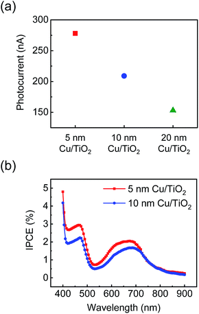 |
| | Fig. 3 (a) Photocurrent and (b) IPCE measured on the Cu/TiO2 diode depending on the thickness of the Cu layer (i.e., 5, 10, and 20 nm). | |
3.4 Enhanced stability of Cu/TiO2 nanodiode with Al2O3 passivation layer
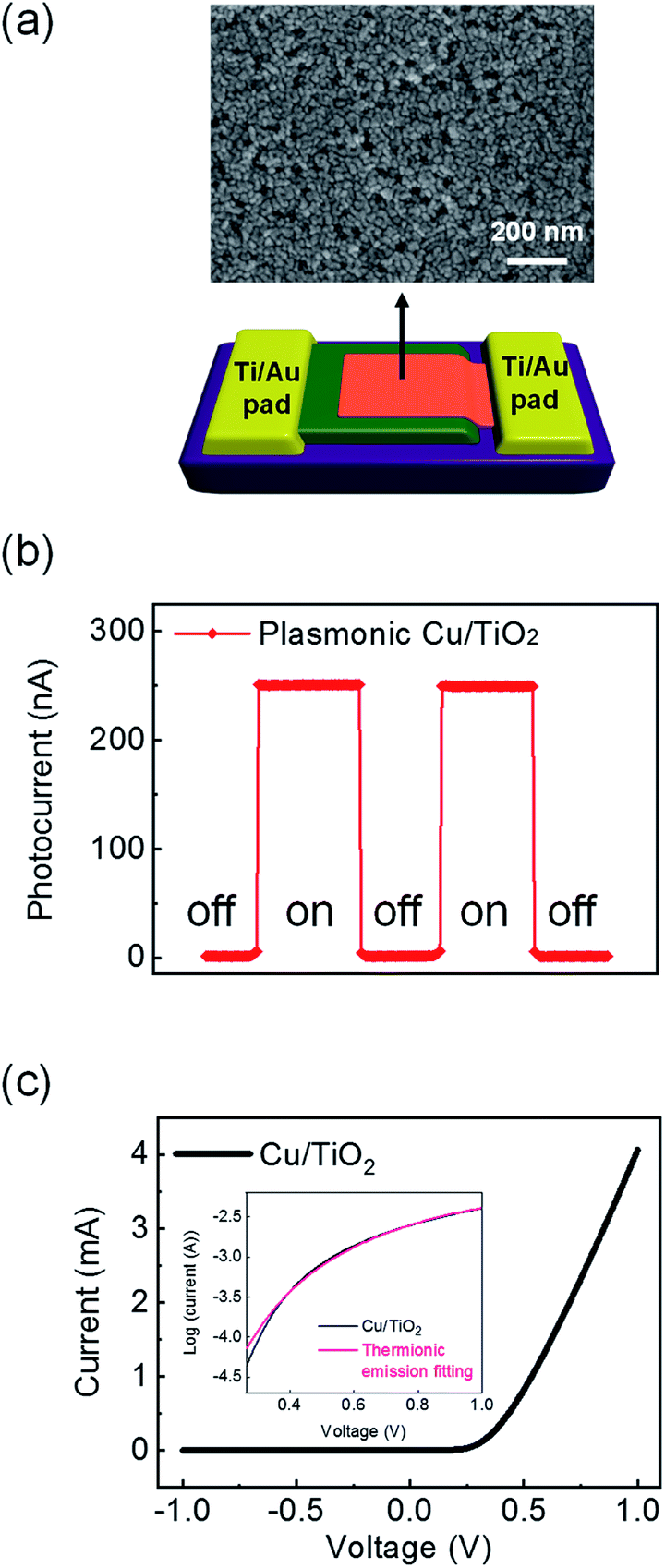
Although copper can exhibit effective plasmonic properties, it has not been widely used because it is easily oxidized in air. Fig. 4(a) shows the degradation of photocurrent with air exposure time measured on the Cu/TiO2 diode with and without a protection layer. Here, an Al2O3 layer was deposited on the Cu film as a protection layer using electron beam evaporation. The photocurrent of the bare Cu/TiO2 diode decreased dramatically to less than 100 nA as it was fully exposed in air. This is because LSPR excitation of the Cu weakened as the Cu layer was oxidized. On the other hand, the photocurrent only slightly decreased, but was saturated at 180 nA with an alumina layer deposited on the copper film. I–V curves were also measured on both diodes (Fig. 4(b)). Based on the measured I–V curves, the Schottky barrier heights of the diodes were calculated using eqn (2). The bare plasmonic Cu/TiO2 showed ϕSB = 0.69 ± 0.01 eV and the Al2O3 coated plasmonic Cu/TiO2 exhibited ϕSB = 0.7 ± 0.01 eV, which means the Schottky barrier height is preserved after deposition of the Al2O3 layer. These results indicate that the alumina film can be used as passivation layer for slowing the degradation of the Cu/TiO2 diode without changing the energetic levels of the diode (i.e., the Schottky barrier height). We note that back-side illumination can lead to enhanced hot electron generation at the metal–dielectric interface. In this case, IPCE will be enhanced if the incident light goes sequentially through the TiO2 to the plasmonic Cu layer, because hot electrons would be mostly generated close to the Schottky barrier height, allowing efficient hot electron capture to occur. Further investigation using a different diode structure could be an interesting subject for a follow-up study.
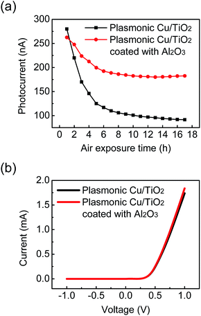 |
| | Fig. 4 (a) Degradation of photocurrent of the plasmonic Cu/TiO2 with and without a protection layer of Al2O3 with air exposure. (b) Current–voltage curves measured on the plasmonic Cu/TiO2 diode (black) and plasmonic Cu/TiO2 diode coated with Al2O3 (red). | |
4. Conclusions
In summary, we fabricated a plasmonic Cu/TiO2 nanodiode to discern hot electron generation via intraband excitation and interband transition on a plasmonic copper film. Based on the electrical measurements, it shows a reasonable Schottky barrier height and photocurrent, which means the diode works well. To distinguish the two different types of transition modes, we measured the IPCE. The plasmonic Cu/TiO2 diode has two distinct IPCE peaks at specific photon energies that are identical to the LSPR absorbance peak and absorbance region for interband transition. However, in the case of the plasmonic Au/TiO2 diode, it only exhibits an intraband transition IPCE peak, while the absorbance spectrum shows both intraband excitation and interband transition. This is because Au has a greater interband transition energy and Schottky barrier height with TiO2 than Cu, which leads to inefficient hot electron extraction from the interband transition. Lastly, we demonstrate a much more stable plasmonic Cu/TiO2 diode in air by depositing an Al2O3 film without changing the Schottky barrier height. These findings imply that there are two different hot electron generation mechanisms in plasmonic metals (intraband excitation and interband excitation), but they can only be detected when the metals absorb incident photons and the excited hot electrons possess sufficient energy to be extracted. Moreover, we expect the stabilized plasmonic properties of Cu with alumina film deposition can suggest designs for efficient Cu-based plasmonic photovoltaics.
Conflicts of interest
There are no conflicts to declare.
Acknowledgements
This work was supported by the Institute for Basic Science (IBS) [IBS-R004].
Notes and references
- C. Clavero, Nat. Photonics, 2014, 8, 95–103 CrossRef CAS.
- L. Novotny and N. van Hulst, Nat. Photonics, 2011, 5, 83–90 CrossRef CAS.
- H. A. Atwater and A. Polman, Nat. Mater., 2010, 9, 205–213 CrossRef CAS PubMed.
- W. R. Erwin, H. F. Zarick, E. M. Talbert and R. Bardhan, Energy Environ. Sci., 2016, 9, 1577–1601 RSC.
- P. Christopher, H. L. Xin and S. Linic, Nat. Chem., 2011, 3, 467–472 CrossRef CAS PubMed.
- U. Aslam, V. G. Rao, S. Chavez and S. Linic, Nat. Catal., 2018, 1, 656–665 CrossRef.
- Y. Tian and T. Tatsuma, Chem. Commun., 2004, 16, 1810–1811 RSC.
- Y. Tian and T. Tatsuma, J. Am. Chem. Soc., 2005, 127, 7632–7637 CrossRef CAS PubMed.
- M. W. Knight, H. Sobhani, P. Nordlander and N. J. Halas, Science, 2011, 332, 702–704 CrossRef CAS PubMed.
- S. Linic, P. Christopher and D. B. Ingram, Nat. Mater., 2011, 10, 911–921 CrossRef CAS PubMed.
- X. G. Li, D. Xiao and Z. Y. Zhang, New J. Phys., 2013, 15, 023011 CrossRef.
- J. Y. Park, L. R. Baker and G. A. Somorjai, Chem. Rev., 2015, 115, 2781–2817 CrossRef CAS PubMed.
- C. Lee, I. I. Nedrygailov, Y. K. Lee, C. Ahn, H. Lee, S. Jeon and J. Y. Park, Nanotechnology, 2015, 26, 445201 CrossRef PubMed.
- E. W. McFarland and J. Tang, Nature, 2003, 421, 616–618 CrossRef CAS PubMed.
- Y. K. Lee, H. Lee, C. Lee, E. Hwang and J. Y. Park, J. Phys.: Condens. Matter, 2016, 28, 254006 CrossRef PubMed.
- J. Lehmann, M. Merschdorf, W. Pfeiffer, A. Thon, S. Voll and G. Gerber, Phys. Rev. Lett., 2000, 85, 2921–2924 CrossRef CAS PubMed.
- G. L. Eesley, Phys. Rev. B, 1986, 33, 2144–2151 CrossRef CAS.
- M. Bernardi, J. Mustafa, J. B. Neaton and S. G. Louie, Nat. Commun., 2015, 6, 7044 CrossRef CAS.
- R. Sundararaman, P. Narang, A. S. Jermyn, W. A. Goddard and H. A. Atwater, Nat. Commun., 2014, 5, 5788 CrossRef CAS.
- A. M. Brown, R. Sundararaman, P. Narang, W. A. Goddard and H. A. Atwater, ACS Nano, 2016, 10, 957–966 CrossRef CAS PubMed.
- Y. K. Lee, C. H. Jung, J. Park, H. Seo, G. A. Somorjai and J. Y. Park, Nano Lett., 2011, 11, 4251–4255 CrossRef CAS PubMed.
- C. Lee, H. Choi, I. I. Nedrygailov, Y. K. Lee, S. Jeong and J. Y. Park, ACS Appl. Mater. Interfaces, 2018, 10, 5081–5089 CrossRef CAS PubMed.
- G. A. Somorjai, H. Frei and J. Y. Park, J. Am. Chem. Soc., 2009, 131, 16589–16605 CrossRef CAS PubMed.
- B. Y. Zheng, H. Q. Zhao, A. Manjavacas, M. McClain, P. Nordlander and N. J. Halas, Nat. Commun., 2015, 6, 7797 CrossRef PubMed.
- T. Yamaguchi, E. Kazuma, N. Sakai and T. Tatsuma, Chem. Lett., 2012, 41, 1340–1342 CrossRef CAS.
- Q. C. Sun, Y. C. Ding, S. M. Goodman, H. H. Funke and P. Nagpal, Nanoscale, 2014, 6, 12450–12457 RSC.
- H. Lee, Y. K. Lee, E. Hwang and J. Y. Park, J. Phys. Chem. C, 2014, 118, 5650–5656 CrossRef CAS.
- Y. K. Lee, J. Lee, H. Lee, J. Y. Lee and J. Y. Park, Appl. Phys. Lett., 2013, 102, 123112 CrossRef.
- P. E. Laibinis and G. M. Whitesides, J. Am. Chem. Soc., 1992, 114, 9022–9028 CrossRef CAS.
- F. Grillo, D. W. Tee, S. M. Francis, H. A. Fruchtl and N. V. Richardson, J. Phys. Chem. C, 2014, 118, 8667–8675 CrossRef CAS.
- P. C. Hsu, H. Wu, T. J. Carney, M. T. McDowell, Y. Yang, E. C. Garnett, M. Li, L. B. Hu and Y. Cui, ACS Nano, 2012, 6, 5150–5156 CrossRef CAS PubMed.
- J. Li, J. W. Mayer and E. G. Colgan, J. Appl. Phys., 1991, 70, 2820–2827 CrossRef CAS.
- J. J. Garramone, J. R. Abel, I. L. Sitnitsky, L. Zhao, I. Appelbaum and V. P. LaBella, Appl. Phys. Lett., 2010, 96, 062105 CrossRef.
|
| This journal is © The Royal Society of Chemistry 2019 |
Click here to see how this site uses Cookies. View our privacy policy here. 
 Open Access Article
 This Open Access Article is licensed under a Creative Commons Attribution-Non Commercial 3.0 Unported Licence
 *abc
*abc