DOI:
10.1039/C9RA02494H
(Paper)
RSC Adv., 2019,
9, 16431-16438
High-aspect-ratio mushroom-like silica nanopillars immersed in air: epsilon-near-zero metamaterials mediated by a phonon-polaritonic anisotropy†
Received
3rd April 2019
, Accepted 20th May 2019
First published on 28th May 2019
Abstract
Epsilon-near-zero metamaterials offer opportunities for intriguing electromagnetic-wave phenomena. Here we experimentally demonstrate that silica perpendicular nanopillars immersed in air exhibit a uniaxial epsilon-near-zero response mediated by phonon polaritons in the mid-infrared range. Unique mushroom-shaped heads on nanopillars play a crucial role to realize SiO2 metamaterials over a large area in our self-assembled fabrication process with block copolymers, polystyrene-block-poly(dimethylsiloxane) (PS-b-PDMS). SiO2 nanopillars having heights of 80 nm, 200 nm, and 300 nm (aspect ratios up to ∼13) are obtained after calcination at 450 °C and the electromagnetic responses are evaluated using a mid-infrared ellipsometric apparatus. For nanopillars with 200 nm height, the permittivity of the perpendicular component ε⊥ approaches to near zero (0.2) while the parallel component ε‖ shows a value of 1.8. The measured uniaxial epsilon-near-zero responses are excellently reproduced by the effective medium theory. Our results, therefore, indicate that SiO2 nanopillars/air uniaxial epsilon-near-zero metamaterials in the mid-infrared range can be amenable to large scale fabrication.
1 Introduction
Researchers have designed electromagnetic metamaterials with unconventional permittivity and permeability values in various frequency ranges. Epsilon-near-zero metamaterials are unique class of materials, which enable the permittivity values lower than that of the free-space.1 They have realized various applications ranging from perfect imaging systems,2 waveform shaping,3 light tunnelling,4,5 perfect absorption,6 and spontaneous emission enhancement.7 Sometimes epsilon-near-zero metamaterials are designed to have anisotropic8,9 or more specifically uniaxial permittivities,10 i.e., the permittivity component in the direction perpendicular to the film is different from that in the direction parallel to the film. Metal and dielectric films are stacked alternately to achieve an epsilon-near-zero permittivity in the parallel direction, and that has been utilized to control thermal emission11 and optical response.12 Alternatively, metallic nanopillar arrays can achieve a uniaxial anisotropy with an epsilon-near-zero permittivity in the perpendicular direction. One pioneering work is Au nanorod arrays obtained by electroplating in porous anodic alumina oxide (AAO) templates.13–16 The Au nanorods also realize the polarization converters17 because the phase delay between p-polarized (perpendicular) and s-polarized (parallel) light is significantly different.
Surface phonon polaritons observed in polar materials, such as hexagonal boron nitride (hBN), SiC, and SiO2, provide strong light–matter interaction in the mid-infrared wavelength range.18–24 Of these materials, SiO2 is a prominent candidate due to ease of synthesis and its numerous potential applications. SiO2 has been widely explored for various application scenarios, such as thermal emission control,25,26 superlenses,27,28 and biosensing.29 Particularly, for thermal emission, when one of the components in such metamaterials is air with small thermal conductivity or vacuum with no thermal conductivity, one can expand design variation in tailoring electromagnetic waves.
In spite of its importance for numerous applications, the mid-infrared device fabrication often suffers from complicated top-down procedures, which are relatively expensive and time-consuming. Self-assembly of block copolymers provides periodically ordered patterns on substrates with relatively simple and low-cost manners.30–32 In these block copolymers, dissimilar polymer chains are covalently linked to each other, and form microphase-separated structures at a molecular level. The long-range periodicity of the obtained microphase-separated structures is greatly enhanced by various external fields, such as vapor33,34 or thermal35 annealing. The formed microphase has been utilized as nanomasks for the subsequent microfabrication,36 profiting from the fact that the pattern feature size is well below the conventional photolithography. A number of well-ordered microphase structures have been realized including in-plane cylinders,37,38 perforated lamella, and vertical cylinders.39,40 Vertical cylinders based on the self-assembly of block copolymers are attracting of great interest because they can be a viable solution to fabricate metamaterials, leading to observe epsilon-near-zero behaviours.
Previously, we have reported a fabrication of SiO2 perpendicular pillar arrays from self-assembled block copolymers, polystyrene-block-poly(dimethylsiloxane) (PS-b-PDMS), using solvent annealing and several etching steps.41 We have speculated that the unique mushroom-shaped heads on nanopillars play a crucial role to maintain a hexagonal regularity during removal of organic components, which was yielded by O2-RIE. The obtained perpendicular pillars are expected to be a platform for SiO2 metamaterials or nanophotonic devices, but its possibility has not been investigated. In this paper, we report a uniaxial epsilon-near-zero behaviour enabled by self-assembled silica nanopillar arrays immersed in air. The electromagnetic response is evaluated at each etching step and the route for SiO2 metamaterials is clearly presented. Mid-infrared ellipsometry has been performed to characterize the effective permittivity of the SiO2 nanopillar arrays. The results validate that self-assembly of block copolymers enables to fabricate metamaterials, having a uniaxial epsilon-near-zero characteristic. The measured uniaxial epsilon-near-zero responses are excellently reproduced by the effective medium theory using retrieved permittivity parameters. We have to mention that there are several pioneering works on manipulating heat flow. Recently, thermal emission and conduction,42 or thermal conduction and convection43 are simultaneously engineered. They have demonstrated sophisticated ways to control two thermal properties out of three (i.e. thermal emission, conduction and convection) and realized promising thermal designs. In this work, we focus on engineering electromagnetic responses (thermal emission) using SiO2 nanopillar arrays with unique mushroom-shaped heads. It would be a great challenge to control two thermal properties with the specific SiO2 metamaterials, however the idea is beyond the scope of this study. The effort to utilize our SiO2 metamaterials is underway to propose an advantageous thermal and optical designs.
2 Experimental
2.1 Pattern formation of mushroom-like silica nanopillars
The overall preparation process of SiO2 cylinder arrays is shown in Fig. 1. Firstly, cylindrical patterns have been formed from the spin-casted film with phase composition of 3–8 wt% PS-b-PDMS dissolved in THF. After solvent annealing in chloroform vapor for 90 min, CF4/O2 RIE (reactive ion etching) has been applied under a CF4 flow rate of 0.1 Pa m3 s−1 and an O2 flow rate of 0.17 Pa m3 s−1 for 60 s at a power of 200 W and chamber pressure of 16 Pa in the case of route B in Fig. 1. With regard to CF4/O2 RIE, the method established by Son et al.39 was modified. O2 plasma treatment has been applied to the film using a plasma reactor (PR300, Yamato Science Co. Ltd.) at 100 W under an O2 flow rate of 0.08 Pa m3 s−1, followed by calcination at 450 °C. The same O2 plasma process has been carried out without O2 RIE on the film fabricated via route A. For route C, the film was calcined at 450 °C after continuous CF4/O2 RIE (without O2 plasma). RIE system (RIE-10NR, Samco Inc.) was employed in this study.
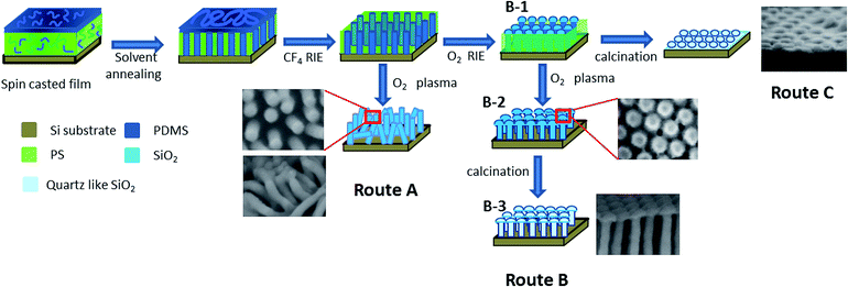 |
| | Fig. 1 Schematic of fabrication routes of SiO2 nanopillar arrays depending on the sequential etching process. | |
2.2 Ellipsometric measurement
We employed ellipsometric technique to evaluate SiO2 nanopillar arrays with the unique mushroom-shaped heads. Ellipsometry is a well-established method to characterize optical responses of thin films.44 In ellipsometry, a difference in light reflection of p- and s-polarizations is detected as the changes in a polarization state. The samples were measured by a mid-infrared ellipsometric spectrometer (IR-VASE, J. A. Woollam). The measured results were represented by two values, namely Ψ and Δ as:| |
 | (1) |
| |
 | (2) |
where rp and rs are the Fresnel reflection coefficients in p- and s-polarizations. Ψ and Δ represent relative amplitude and phase difference of the p-polarized reflection coefficient to the s-polarized counterpart. Thus the tilt of the samples and other artifacts are easily compensated in measurement results and how the permittivities of our samples relate to the two polarizations is observed through eqn (1) and (2). The absolute values of Ψ and Δ do not have significant meaning, thus an optical model is required to analyse measurement data. In this paper, we mainly discuss the frequency responses of our samples with eqn (1) and (2) after showing the p-polarized reflection coefficients (Fig. 2).
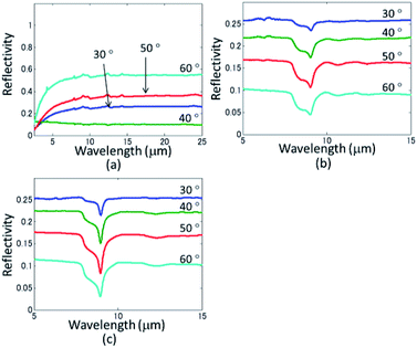 |
| | Fig. 2 P-polarized reflection spectra using FTIR spectroscopy during transition after (a) CF4 and O2 RIE, followed by (b) O2 plasma, and (c) calcination at 450 °C. | |
2.3 Characterization
SEM images of surface and cross-sectional views were obtained using field-emission scanning electron microscopes (Hitachi S-4800 and S-5500, respectively). FT-IR (Fourier-transformed infrared) spectroscopy was conducted on an FT-IR spectrometer (Nicolet iS50, Thermo Fisher Scientific, Inc.) to investigate compositional change of the nanopillars during the fabrication steps. The incident angle from the surface normal was changed from 30° to 60° at every 10°. The finite integration-technique based simulator CST Microwave Studio was utilized in the frequency domain for electromagnetic simulations of our nanostructures. The electromagnetic fields were excited and monitored by Floquet ports, and the reflection coefficients were calculated. From eqn (1) and (2) with the simulated reflection coefficients, we obtained Ψ and Δ.
3 Results and discussion
3.1 Changes of electromagnetic status depending on process
Firstly, we measured FTIR spectra on SiO2 nanopillars obtained thorough route B in Fig. 1 to investigate the electromagnetic status at each etching step. Fig. 2 shows the obtained results of SiO2 nanopillars fabricated from a 5 wt% PS-b-PDMS solution via route B in Fig. 1.
In Fig. 2(a), flat reflection spectra were observed in the wavelength range from 7 to 20 μm after CF4 and O2 RIE (B-1 in Fig. 1). Then in Fig. 2(b), a broad dip has emerged at around 8.5 μm after O2 plasma (B-2 in Fig. 1) at all angles. The obtained dips correspond to fused quartz phonons, which induce an epsilon-near zero response. But at this stage, a hallo-like dent was also detected at around 11 μm, indicating amorphous silica structure remains to some extent. Upon calcination at 450 °C (Fig. 2(c)), the dips at around 8.5 μm become sharper and the hallo-like dent patterns at 11 μm disappear because the permittivity of the SiO2 nanopillars approaches to that of fused quartz. These measured results indicate that calcination step, which is newly added in this study, enables fabrication of the fused quartz-like SiO2 nanopillars from the self-assembly of PS-b-PDMS. Then, we investigate morphological change of SiO2 nanopillars upon the sequential etching steps using SEM (Fig. 3). As was indicated in the previous report, O2 RIE partially melts the thin surface layer of PDMS pillars and yields mushroom-like heads, which is supposed to play a key role to maintain a hexagonal regularity during removal of organic components by O2 plasma.41 The morphology is well observed in cross-sectional SEM images (Fig. 3(a, c and e)) and more detailed explanation for the formation of mushroom-like heads can be found in elsewhere.45 We newly find that mushroom-like heads are effective to maintain the regularity of the pillar structure even at 450 °C calcination. No significant degradation in the hexagonal regularity during calcination is seen in Fig. 3(e) and an average height of 200 nm, corresponding to an aspect ratio of 8.7 unveils for the fused quartz-like SiO2 nanopillars.
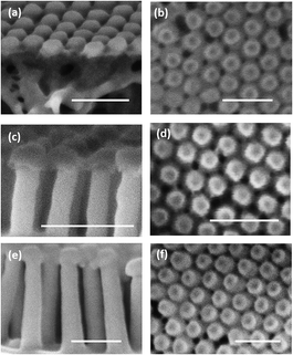 |
| | Fig. 3 (a, c and e) Cross-sectional and (b, d and f) top view SEM images showing the emergence and maintenance of perpendicular cylinders from the 5 wt% PS-b-PDMS solution via route B in Fig. 1. Images were taken (a and b) after CF4 and O2 RIE (B-1 in Fig. 1), (c and d) after O2 plasma for 240 s (B-2 in Fig. 1), and (e and f) after calcination at 450 °C (B-3 in Fig. 1). The scale bars indicate 100 nm, respectively. | |
Here, we investigate other conceivable routes for SiO2 metamaterials consisting from nanopillar arrays (route A and route C in Fig. 1). In the route A, the pillar arrays are fabricated without O2 RIE, leading to significant deterioration of the hexagonal regularity upon the O2 plasma treatment, which is shown in Fig. 4. In the case that the O2 plasma process has been conducted with a short duration (60 s), PS remains in the bottom of the pillars as shown in Fig. 4(a), which acts as a foundation to maintain the hexagonal regularity, instead of adhesion between the adjutant mushroom-like heads (Fig. 3). Then we have lengthened the duration of O2 plasma (120 s), and found that the regularity of the remaining pillar arrays was significantly lowered as the organic remnants were removed (Fig. 4(b)). It should be noted that the higher the PDMS pillars, the more severely the regularity of nanopillar arrays is deteriorated. The observation in this study verified our concept, that the mushroom-like heads are essential on fabrication of the fused quartz-like SiO2 nanopillars using self-assembly of PS-b-PDMS. One may doubt a necessity of the O2 plasma treatment to remove organic remnants and fully oxide the PDMS to the fused quartz. Calcination at 450 °C immediately after the continuous RIEs (route C in Fig. 1) can provide a mushroom-like heads as well as remove the organic components. However, nanopillars with high aspect ratios are not obtained. Nanopillars seem to collapse and form dot arrays upon calcination without the O2 plasma process (Fig. S1 in ESI†). O2 plasma is frequently used for surface modification of plastics, and increase of oxygen content on the surface was reported.46 The thickness of surface oxide layers was studied using XPS depth-profiling technique (Fig. S2 in ESI†). The thick oxide layer was yielded upon the O2 plasm process, which can act as a protecting substance during calcination at 450 °C. It is obvious that the route B in Fig. 1 is an only solution to fabricate SiO2 nanopillar arrays having a hexagonal regularity and fused-quartz-like electromagnetic states.
 |
| | Fig. 4 Cross-sectional SEM images showing the emergence of straight perpendicular cylinders from a 3 wt% PS-b-PDMS solution via route A in Fig. 1. O2 plasma treatment was conducted for (a) 60 s and (b) 120 s. The inset in (a) is a top-view image of the straight shape pillars. The scale bars indicate 100 nm. | |
3.2 Ellipsometry measurement and prediction of the optical anisotropy
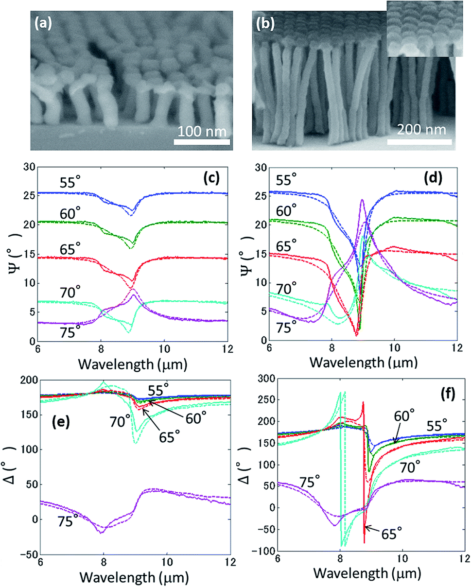
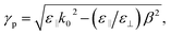
We evaluated the fused-quartz-like nanopillar arrays fabricated from the 5% PS-b-PDMS solution. Ellipsometrical parameters Ψ and Δ were measured by the mid-infrared ellipsometry apparatus and the results were depicted in Fig. 5. Data from 5 different angles, namely 55°, 60°, 65°, 70°, and 75° have been presented. In the spectra for Ψ, the peaks are negative in the case that the incident angle is smaller than the Brewster angle of the silicon and air interface (73°). A strong resonant mode was clearly identified at around 9 μm in Fig. 5(a) which was induced by phonon polariton excitations. The changes in Ψ and Δ come from the phonon polariton excitation in our nanopillars that is seen in Fig. 2. As pointed out in the previous section, the clear dips are detected in the reflectivity (Fig. 2) where the resonant mode is observed in Fig. 5. Note that the depolarization factors measured in the optical ellipsometry are also shown in Fig. S3 in ESI,† and it is smaller than 2% in the wavelength range of interest.
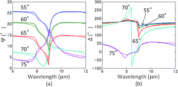 |
| | Fig. 5 Ellipsometrically measured and calculated parameters Ψ (a) and Δ (b). Data are obtained at angles of 55° (blue line), 60° (green line), 65° (red line), 70° (cyan line), and 75° (purple line), respectively. Solid curves are measured results and dotted curves are predicted results by the effective medium theory. | |
Then, we will retrieve a uniaxial permittivity from the measured Ψ and Δ by utilizing the effective medium theory. The permittivity of SiO2 (εQ) is expressed by the Lorentz model.
| |
 | (3) |
where
ω is the angular frequency,
ε∞ is the permittivity at infinite frequency,
A1,2 is the oscillator strength,
ω01,02 is the resonance frequency, and
Γ1,2 is the damping rates for two-poles. Here, we regard the arrays of SiO
2 nanopillars as a thin film with an anisotropic permittivity according to the effective medium theory. The permittivity components in the directions of perpendicular (
ε⊥), and parallel (
ε‖) to the film surface are given by
47| | |
ε⊥ = fεQ + εA (1 − f),
| (4) |
| |
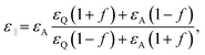 | (5) |
where
f is the volume fraction of the SiO
2 nanopillars within the film, and
εA is the permittivity of air. Together with these values and the height of the SiO
2 nanopillars estimated from the SEM observation, we fit a set of permittivity parameters to explain the experimental results (Table S1 in ESI
†). The calculated
Ψ and
Δ, based on the fitted parameters, are shown as the dotted lines in
Fig. 5. The solid and the dotted curves agree quite well, indicating that the experimental results are well reproduced by the calculated values over the entire substrate.
The predicted permittivities based on the effective medium theory are shown in Fig. 6. We observe an anisotropic nature in the permittivity in Fig. 6(a), where the perpendicular component ε⊥ approaches 0.2 with a parallel component ε‖ of 1.8. The results validate that self-assembly of block copolymers enables to realize a phonon-polaritonic anisotropy, which facilitates uniaxial epsilon-near-zero metamaterials. We have also predicted intrinsic permittivity εQ as shown in Fig. 6(b). It is clear that the resonant wavelength of the obtained nanopillars is almost identical to that of the reported fused quartz, though the resonant amplitude of the nanopillars is smaller than the reported value. This phenomenon may come from the low calcination temperature in this study (450 °C), which leads to a weaker SiO2 bond than nominal fused quartz substrate.
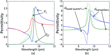 |
| | Fig. 6 Predicted permittivities of SiO2 nanopillars. (a) Perpendicular component (blue solid curve: real part, and green dashed curve: imaginary part) and the parallel component (red solid curve: real part, and cyan dashed curve: imaginary part) of the uniaxial permittivity of the SiO2 nanopillars. (b) Intrinsic permittivity of the SiO2 nanopillars (thick blue curve: real part, and thick green dashed curve: imaginary part). The permittivity of fused quartz in ref. 48 is shown for comparison (thin blue curve: real part, and thin green dashed curve: imaginary part). | |
3.3 Ellipsometric measurements on nanopillars having heights of 80 and 300 nm
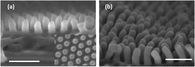
The SiO2 nanopillars with other heights have been also measured by the mid-infrared ellipsometric apparatus to verify our calculations. Changing the content of PS-b-PDMS in the spin-casting solution allows us to tune the height of the SiO2 nanopillars easily via route B in Fig. 1. As was mentioned in the previous section (3.2), the SiO2 nanopillars with a height of around 200 nm are obtained from the 5 wt% PS-b-PDMS solution. Meanwhile, the compositional weight percentages of 3 wt% and 8 wt%, respectively, realize the pillars whose heights are 80 nm and 300 nm as shown in Fig. 7(a) and (b). In both cases, perpendicular cylinder arrays having mushroom-like heads are clearly observed even after 450 °C calcination. An aspect ratio as high as 13 is achieved from the 8 wt% PS-b-PDMS solution after calcination (Fig. 7(b)).
 |
| | Fig. 7 SEM images of the SiO2 nanopillars fabricated from (a) 3 wt% and (b) 8 wt% PS-b-PDMS solutions. Inset in (b) represents the adhesion between mushroom-like heads of adjacent pillars. Ellipsometrically measured and calculated parameters Ψ (c and d) and Δ (e and f) for films fabricated from 3 wt% (c and e) and 8 wt% (d and f) PS-b-PDMS solutions. Data are obtained at angles of 55° (blue line), 60° (green line), 65° (red line), 70° (cyan line), and 75° (purple line), respectively. Solid curves are measured results and dotted curves are predicted results by the effective medium theory. | |
The permittivities for the films fabricated from 3 and 8 wt% of PS-b-PDMS solutions are modelled by the same manner retrieved in the film prepared from the 5 wt% solution. Ellipsometrically measured parameters Ψ and Δ are compared with those obtained from the predicted models (Fig. 7(c–f)). The results show that the modelled permittivity well explains the obtained cylinder arrays with each height. It is well observed that the measured peaks and the dips become steeper as the pillar height increases due to the enhancement of the anisotropy. The experimental results are well reproduced on calculations for SiO2 nanopillars with different heights, which corroborates our predicted model strongly.
Importance of the high-aspect ratio upon optical anisotropy which can expand material designs is shown in previous discussion. Additionally, we would like to compare directly the impact of the aspect ratio of the SiO2 nanopillar arrays on the electromagnetic responses. Uniaxial permittivity media provide the feature of different wavevectors for p- and s-polarized waves. Using the retrieved permittivity components in Fig. 6, we calculate the optical lengths of p- and s-polarized waves along the nanopillars. Fig. 8 shows the relative optical length of the p-polarized wave to the s-polarized wave, the real part of γph–γsh with pillar heights of h = 80 nm, 200 nm, and 300 nm, respectively. In this relation, the perpendicular wavevector components for p-polarization (γp) and s-polarization (γs) are expressed as:
| |
 | (6) |
| |
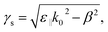 | (7) |
where
β and
k0 are the lateral wavevector component and the free space wavelength. We see that the optical length of the p-polarized wave can be shorter (
ε‖ >
ε⊥) [longer (
ε‖ <
ε⊥)] than that of the s-polarized wave around the wavelength range of phonon polariton excitation, and the optical length difference is enhanced as the pillar height increases.
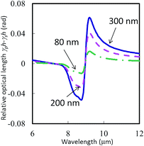 |
| | Fig. 8 Relative optical length of the p-polarized wave to the s-polarized wave in the nanopillar array with heights of 80 nm, 200 nm and 300 nm, respectively. Data are calculated at an angle of 65°. | |
3.4 Validity of the ellipsometric values based on effective medium theory by CST microwave studio simulation
The effective medium theory has been known to work well in the case that the structure is regarded as homogenous medium.49 In this study, the pitch between the pillars is much smaller than the wavelength of interest, while the pillar heights are smaller than the incident wavelength. Thus, we try to validate the calculations utilizing the effective medium theory and CST microwave studio. The results are shown in Fig. 9. In the CST microwave studio simulation, the model is composed of the infinite substrate, pillar array with the hexagonal arrangement, and infinite atmosphere above the structure. The electromagnetically simulated structure is shown in the inset of Fig. 9(d). Note that the mushroom-like head has little influence on the electromagnetic response because the size is small enough as compared to the wavelength of light. There was no significant difference in the calculated results using the effective medium theory (Fresnel equations) and CST microwave studio. Only a slight difference between these two simulations, less than 0.5°, can be found in a magnified image (Fig. 9(c) and (d)). The calculation based on CST Microwave studio reflects Maxwell's equation accurately, without using approximations.50 Thus we have concluded that Fresnel calculation based on the effective medium theory well provides sufficient precision compared to full-wave simulation.
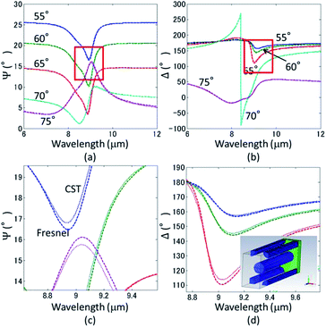 |
| | Fig. 9 Comparison of (a) and (c) ellipsometric spectra Ψ and (b) and (d) Δ obtained by CST microwave studio (dotted curves) and the effective medium theory (bold dotted curves). The pillar height is set at 200 nm. (c) and (d) are the magnified images of the plots indicated by the red squares in (a) and (b). The inset in (d) depicts the simulation model of SiO2 nanopillars in CST microwave studio. | |
4 Conclusions
To conclude, we have demonstrated a bottom-up approach for the large-scale fabrication of metamaterials consisting of SiO2 nanopillar immersed in air with a cost-effective manner. Self-assembly of PS-b-PDMS block copolymers enables to form uniaxial epsilon-near zero metamaterials which are mediated by phonon-polaritons in the mid infrared wavelength region. Unique mushroom-like heads on SiOx perpendicular cylinders play a key role to realize SiO2 nanopillars having the similar permittivity as that of the fused quartz over a large area. Nanopillars having heights of 80, 200, and 300 nm are fabricated and the mid-infrared ellipsometry is conducted. The experimental values are well reproduced on the calculated results utilizing the effective medium theory for nanopillars with various heights. The observed agreements indicate an optical anisotropy of the SiO2 nanopillars. Furthermore, the calculation based on the effective medium theory is validated by the CST microwave studio simulation. Due to the intrinsic property of block copolymers, structural parameters, including the size and spacing of SiO2 nanopillars, can be tailored. Such a character may allow us to control the volume fraction of nanopillars and to design metamaterials with hyperbolic permittivity. This study can potentially be used in a variety of optical and thermal applications, with cost-effective manner, and enables to contribute the progress of nanophotonics to benefit our society.
Conflicts of interest
There are no conflicts of interest to declare.
Acknowledgements
The authors are grateful to K. Nakai, K. Kitazumi and Dr H. Yoda for technical supports and fruitful discussions. The authors also acknowledge Dr H. Wakayama and K. Yatsugi for helpful supports. This work was partially supported by the Toyota Technological Institute Nano Technology Hub of the ‘Nanotechnology Platform Project’ sponsored by the Ministry of Education, Culture, Sports, Science and Technology (MEXT), Japan.
Notes and references
- I. Liberal and N. Engheta, Nat. Photonics, 2017, 11, 149 CrossRef CAS.
- G. Castaldi, S. Savoia, V. Galdi, A. Alù and N. Engheta, Phys. Rev. B: Condens. Matter Mater. Phys., 2012, 86, 115123 CrossRef.
- A. Alù, M. G. Silveirinha, A. Salandrino and N. Engheta, Phys. Rev. B: Condens. Matter Mater. Phys., 2007, 75, 155410 CrossRef.
- B. Edwards, A. Alù, M. E. Young, M. Silveirinha and N. Engheta, Phys. Rev. Lett., 2008, 100, 033903 CrossRef PubMed.
- R. Liu, Q. Cheng, T. Hand, J. J. Mock, T. J. Cui, S. A. Cummer and D. R. Smith, Phys. Rev. Lett., 2008, 100, 023903 CrossRef PubMed.
- S. Feng and K. Halterman, Phys. Rev. B: Condens. Matter Mater. Phys., 2012, 86, 165103 CrossRef.
- S. Vassant, A. Archambault, F. Marquier, F. Pardo, U. Gennser, A. Cavanna, J. L. Pelouard and J. J. Greffet, Phys. Rev. Lett., 2012, 109, 237401 CrossRef CAS PubMed.
- L. Sun, S. Feng and X. Yang, Appl. Phys. Lett., 2012, 101, 241101 CrossRef.
- J. Luo, P. Xu, H. Chen, B. Hou, L. Gao and Y. Lai, Appl. Phys. Lett., 2012, 100, 221903 CrossRef.
- L. V. Alekseyev, E. E. Narimanov, T. Tumkur, H. Li, Y. A. Barnakov and M. A. Noginov, Appl. Phys. Lett., 2010, 97, 131107 CrossRef.
- P. N. Dyachenko, S. Molesky, A. Y. Petrov, M. Störmer, T. Krekeler, S. Lang, M. Ritter, Z. Jacob and M. Eich, Nat. Commun., 2016, 7, 11809 CrossRef CAS PubMed.
- J. Gao, L. Sun, H. Deng, C. J. Mathai, S. Gangopadhyay and X. Yang, Appl. Phys. Lett., 2013, 103, 051111 CrossRef.
- D. P. Lyvers, J. M. Moon, A. V. Kildishev, V. M. Shalaev and A. Wei, ACS Nano, 2008, 2, 2569–2576 CrossRef CAS PubMed.
- L. Dusan, J. G. Shapter, J. G. Mitchell and N. H. Voelcker, Nanotechnology, 2005, 16, 2275 CrossRef PubMed.
- E. Paul, W. R. Hendren, R. Atkinson, G. A. Wurtz, W. Dickson, A. V. Zayats and R. J. Pollard, Nanotechnology, 2006, 17, 5746 CrossRef.
- A. V. Kabashin, P. Evans, S. Pastkovsky, W. Hendren, G. A. Wurtz, R. Atkinson, R. Pollard, V. A. Podolskiy and A. V. Zayats, Nat. Mater., 2009, 8, 867–871 CrossRef CAS PubMed.
- P. Ginzburg, F. J. Rodríguez Fortuño, G. A. Wurtz, W. Dickson, A. Murphy, F. Morgan and R. J. Pollard, et al., Opt. Express, 2013, 21, 14907–14917 CrossRef CAS PubMed.
- P. Li, X. Yang, T. W. W. Maß, J. Hanss, M. Lewin, A.-K. U. Michel, M. Wuttig and T. Taubner, Nat. Mater., 2016, 15, 870–875 CrossRef CAS PubMed.
- R. Hillenbrand, T. Taubner and F. Keilmann, Nature, 2002, 418, 159–162 CrossRef CAS PubMed.
- J. D. Caldwell, L. Lindsay, V. Giannini, I. Vurgaftman, T. L. Reinecke, S. A. Maier and O. J. Glembocki, Nanophotonics, 2015, 4, 44–68 CAS.
- F. Neubrech, D. Weber, D. Enders, T. Nagao and A. Pucci, J. Phys. Chem. C, 2010, 114, 7299–7301 CrossRef CAS.
- J.-J. Greffet, R. Carminati, K. Joulain, J.-P. Mulet, S. Mainguy and Y. Chen, Nature, 2002, 416, 61–64 CrossRef CAS PubMed.
- K. Joulain, J.-P. Mulet, F. Marquier, R. Carminati and J.-J. Greffet, Surf. Sci. Rep., 2005, 57, 59–112 CrossRef CAS.
- B. J. Lee and Z. M. Zhang, J. Appl. Phys., 2006, 100, 063529 CrossRef.
- Y. Zhai, Y. Ma, S. N. David, D. Zhao, R. Lou, G. Tan, R. Yang and X. Yin, Science, 2017, 355, 1062–1066 CrossRef CAS PubMed.
- K. Ito, K. Nishikawa, A. Miura, H. Toshiyoshi and H. Iizuka, Nano Lett., 2017, 17, 4347–4353 CrossRef CAS PubMed.
- J. Kyoung, D. J. Park, S. J. Byun, J. Lee, S. B. Choi, S. Park and S. W. Hwang, Opt. Express, 2014, 22, 31875–31883 CrossRef CAS PubMed.
- W. Cai, D. A. Genov and V. M. Shalaev, Phys. Rev. B: Condens. Matter Mater. Phys., 2005, 72, 193101 CrossRef.
- M. P. Schwartz, S. D. Alvarez and M. J. Sailor, Anal. Chem., 2007, 79, 327–334 CrossRef CAS PubMed.
- X. H. Zhang, J. F. Douglas and R. L. Jones, Soft Matter, 2012, 8, 4980–4987 RSC.
- A. H. Gröschel and A. H. E. Müller, Nanoscale, 2015, 7, 11841–11876 RSC.
- Y. Choo, P. W. Majewski, M. Fukuto, C. O. Osuji and K. G. Yager, Nanoscale, 2018, 1, 416–427 RSC.
- X. D. Gu, I. Gunkel, A. Hexemer, W. Y. Gu and T. P. Russell, Adv. Mater., 2014, 26, 273–281 CrossRef CAS PubMed.
- H. K. Choi, J. Gwyther, I. Manners and C. A. Ross, ACS Nano, 2012, 6, 8342–8348 CrossRef CAS PubMed.
- S. Samant, J. Strzalka, K. G. Yager, K. Kisslinger, D. Grolman, M. Basutkar, N. Salunke, G. Singh, B. Berry and A. Karim, Macromolecules, 2016, 49, 8633–8642 CrossRef CAS.
- C. M. Bates, M. J. Maher, D. W. Janes, C. J. Ellison and C. G. Willson, Macromolecules, 2013, 47, 2–12 CrossRef.
- S. O. Kim, H. H. Solak, M. P. Stoykovich, N. J. Ferrier, J. J. de Pablo and P. F. Nealey, Nature, 2003, 424, 411–414 CrossRef CAS PubMed.
- J. Y. Sik, J. H. Lee, J. Y. Lee and C. A. Ross, Nano Lett., 2010, 10, 3722–3726 CrossRef PubMed.
- J. G. Son, K. W. Gotrik and C. A. Ross, ACS Macro Lett., 2012, 1, 1279–1284 CrossRef CAS.
- G. E. Bhoje, T. Koga, M. K. Endoh, K. Kumar and M. Stamm, Soft Matter, 2014, 10, 7753–7761 RSC.
- Y. Yamada, K. Ito, A. Miura, M. Harada, T. Matsunaga, Y. Kato, T. Matsui, H. Iizuka and H. Wakayama, Eur. Polym. J., 2018, 107, 96–104 CrossRef CAS.
- Y. Li, X. Bai, T. Yang, H. Luo and C.-W. Qiu, Nat. Commun., 2018, 9, 273 CrossRef PubMed.
- Y. Li, K.-J. Zhu, Y.-G. Peng, W. Li, T. Yang, H.-X. Xu, H. Chen, X.-F. Zhu, S. Fan and C.-W. Qiu, Nat. Mater., 2019, 18, 48–54 CrossRef CAS PubMed.
- H. Fujiwara, in Spectroscopic Ellipsometry: Principles and Applications, Wiley, UK, 2007 Search PubMed.
- Q. Xia, K. J. Morton, R. H. Austin and S. Y. Chou, Nano Lett., 2008, 8, 3830–3833 CrossRef CAS PubMed.
- J. Hopkins and J. P. S. Badyal, Macromolecules, 1994, 27, 5498–5503 CrossRef CAS.
- J. J. Saarinen, S. M. Weiss, P. M. Fauchet and J. E. Sipe, J. Appl. Phys., 2008, 104, 013103 CrossRef.
- R. Kitamura, L. Pilon and M. Jonas, Appl. Opt., 2007, 46, 8118–8133 CrossRef CAS PubMed.
- T. C. Choy, in Effective Medium Theory, ed. J. Birman, S. F. Edwards, R. Friend, M. Rees, D. Sherrington and G. Veneziano, Oxford Univ. Press, UK, 2nd edn, 2015 Search PubMed.
- N. C. Dyck, R. C. Denomme and P. M. Nieva, J. Phys. Chem. C, 2011, 115, 15225–15233 CrossRef CAS.
Footnote |
| † Electronic supplementary information (ESI) available: SEM images of SiO2 dot arrays without O2 plasma process, XPS depth profiles, depolarization factors, and the calculated Lorentz parameters. See DOI: 10.1039/c9ra02494h |
|
| This journal is © The Royal Society of Chemistry 2019 |
Click here to see how this site uses Cookies. View our privacy policy here. 
 Open Access Article
 This Open Access Article is licensed under a Creative Commons Attribution-Non Commercial 3.0 Unported Licence
 *a,
Atsushi Miuraa and
Hideo Iizuka
*a,
Atsushi Miuraa and
Hideo Iizuka