
 Open Access Article
 This Open Access Article is licensed under a Creative Commons Attribution-Non Commercial 3.0 Unported Licence
Atomic layer deposition and tellurization of Ge–Sb film for phase-change memory applications
Yewon Kim a,
Byeol Hana,
Yu-Jin Kima,
Jeeyoon Shina,
Seongyoon Kima,
Romel Hidayata,
Jae-Min Parka,
Wonyong Kohb and
Won-Jun Lee*a
a,
Byeol Hana,
Yu-Jin Kima,
Jeeyoon Shina,
Seongyoon Kima,
Romel Hidayata,
Jae-Min Parka,
Wonyong Kohb and
Won-Jun Lee*a
aDepartments of Nanotechnology and Advanced Materials Engineering, Sejong University, Seoul 05006, Republic of Korea. E-mail: wjlee@sejong.ac.kr
bUP Chemical Co., Ltd., Pyeongtaek-Si, Gyeonggi-do 17749, Republic of Korea
First published on 3rd June 2019
Abstract
We studied the atomic layer deposition (ALD) and the tellurization of Ge–Sb films to prepare conformal crystalline Ge–Sb–Te (GST) films and to achieve void-free gap filling for emerging phase-change memory applications. ALD Ge–Sb film was prepared by alternating exposures to GeCl2-dioxane and Sb(SiEt3)3 precursors at 100 °C. The growth rate was 0.021 nm per cycle, and the composition ratio of Ge to Sb was approximately 2.2. We annealed the ALD Ge–Sb films with a pulsed feeding of di(tert-butyl)tellurium. The ALD Ge–Sb films turned into GST films by the tellurization annealing. When the tellurization temperature was raised to 190 °C or higher temperatures, the Raman peaks corresponding to Ge–Sb bond and amorphous Ge–Ge bond disappeared. The Raman peaks corresponding to Ge–Te and Sb–Te bonds were evolved at 200 °C or higher temperatures, resulting in the phase transition temperature of 123 °C. At 230 °C or higher temperatures, the entire film was fully tellurized to form a GST film having a relatively uniform composition of Ge3Sb2Te6, and the carbon impurities in the as-deposited ALD Ge–Sb film were eliminated. As the tellurization temperature increases, the volume of the ALD film is expanded owing to the incorporation of tellurium, resulting in complete filling of a trench pattern by GST film after the tellurization at 230 °C.
Introduction
Since the release of commercial phase change random access memory (PCRAM),1 the interest in PCRAM as a nonvolatile memory device has been increasing. In particular, PCRAM is getting attention as a server's storage class memory because of lower latency and higher endurance compared with NAND flash memory. It is also possible to integrate with higher memory densities than dynamic random-access memory (DRAM) devices.2–4 The confined structure can significantly reduce the thermal interference between the memory cells compared to the conventional mushroom structure,5 thereby significantly increasing the memory density. Alternatively, a three-dimensional (3D) vertical PCRAM structure similar to a 3D vertical NAND structure was also proposed.6 Among the phase change materials, Ge–Sb–Te (GST) compounds were widely studied because of their high crystalline temperature and low melting point, resulting in fast switching speed, low operation energy, and high data retention.7–9 Physical vapor deposition (PVD) has been studied as the method of manufacturing GST.10–12 However, it is hard for the conventional PVD techniques to gapfill the confined structure with a phase change material or to prepare a conformal phase change material film on a 3D vertical PCRAM structure. Besides, the conventional sputtering processes using GST targets result in Te-deficient GST films because of the higher volatility of Te element than those of others.13,14 Atomic layer deposition (ALD) of the phase change material is the ideal solution and has been studied for the last decade.15,16Since the introduction of tellurium silyl compounds, ALD studies using chloride precursors and Te silyl precursors have been accelerated.17 The ALD process of the compound thin film having the composition of Ge–Sb–Te ternary system is complicated. Many famous compositions, such as Ge2Sb2Te5, Ge1Sb2Te4, and Ge1Sb4Te7, are located on the pseudo-binary line between GeTe and Sb2Te3. The supercycles of ALD GeTe and ALD Sb2Te3 were reported to prepare Ge2Sb2Te5 film, and ALD GeTe and ALD Sb2Te3 were possible by using a Te silyl precursor with GeCl2-dioxane complex or SbCl3.17,18 However, the composition ratio of Ge to Sb was sensitive to Ge precursor pulse time as well as the ratio of GeTe subcycle.17 Also, the ALD GST films prepared by supercycle were tellurium-deficient and contained oxygen impurity. Due to the oxygen impurity, the crystallization temperature of the film was higher than that of the PVD Ge2Sb2Te5 film.19 Chlorine-free ALD chemistry was reported using Ge(OMe)4, Sb(OEt)3, Te(SiMe3)2, and Sb(SiMe3)3.20 Since the oxidation state of Ge in Ge(OMe)4 is +4, GeTe2 was obtained by alternating exposures to Ge(OMe)4 and Te(SiMe3)2. The Ge2Sb2Te5 film was prepared by supercycles of ALD GeTe2, Sb2Te3, and Sb. Another chlorine-free ALD chemistry was reported using amide compounds of Ge and Sb.21 Tellurium-deficient film was deposited due to the thermal decomposition of the Ge and Sb precursors. Ge2Sb2Te5 film was prepared by supercycles of ALD Ge–Te, Sb–Te, and Te. Tellurium silyl precursor enables low temperature deposition of GeTe, Sb2Te3, Sb and Te. However, the film grows as a low-density amorphous film because the deposition temperature is low.17 This causes volume shrinkage and void formation due to crystallization during PCRAM use.22 When depositing at higher temperatures using a tellurium alkyl precursor, a crystalline thin film is deposited with a rough surface and the seam inside trenches.23
The way of forming a fully-tellurized crystalline GST film is the tellurization annealing of a Ge–Sb film. Tellurization processes have been reported for CdTe photovoltaic,24,25 and Bi2Te3 thermoelectric materials26 to make the stoichiometric telluride films. The metallic films were heat-treated at temperatures of 400 °C or higher in tellurium atmosphere that is formed by sublimation of tellurium powders. The tellurization process of a phase change material has also been reported.27 The GeSb thin film was deposited by chemical vapor deposition (CVD) method and then annealed at temperatures between 230 and 300 °C using di(tert-butyl)tellurium [(tBu)2Te] or di(isopropyl)tellurium [(iPr)2Te2] as the tellurium source gas. However, the details of process condition and the changes in film properties during the tellurization process were not adequately described.
In the present work, we propose the tellurization of an ALD Ge–Sb thin film to achieve void-free gap filling of nanoscaled structures with crystalline GST film for emerging PCRAM applications. This process also can produce thin conformal crystalline GST films over high-aspect ratio patterns. We investigated the deposition characteristics of ALD Ge–Sb using GeCl2-dioxane and Sb(SiEt3)3 precursors at 100 °C. It has been reported that the ALD process of Ge–Sb films is possible, but details were not disclosed.28 We annealed the ALD Ge–Sb films with a pulsed feeding of the tellurium precursor and investigated the composition profile and crystallization temperature of the tellurized film with varying the annealing temperature. In the previous work, we studied the tellurization of sputtered Ge–Sb film.29 Crystalline Ge–Sb–Te films were prepared by adjusting annealing temperature or time. When the ALD Ge–Sb film is tellurized at a higher temperature, the volume is expanded owing to the incorporation of tellurium while being crystallized. We selected tBu2Te as the tellurium source for tellurization annealing because it has high vapor pressure than metallic tellurium and is thermally stable at below 300 °C.30,31 Gap filling of a trench pattern by the ALD and the tellurization was also investigated and discussed.
Experimental
GeCl2-dioxane complex was used as the Ge precursor and Sb(SiEt3)3 was used as the Sb precursor. We used DFT calculations to check the feasibility of the ALD reaction using Dmol3 package of Material studio 7.0 (Accelrys, USA). The generalized gradient approximation (GGA) with the Perdew–Burke–Ernzerhof (PBE)32 were used as exchange–correlation functional and the double numerical polarization (DNP)33 as the basis set. We performed the geometry optimization for all structures of precursors and ALD reaction products and the determined the total energies of the system before and after the ALD reaction.34,35GeCl2-dioxane, Sb(SiEt3)3, and tBu2Te were synthesized and purified to 99% or higher. A showerhead-type ALD reactor (iOV-D100, ISAC Research, Republic of Korea) was used for the deposition and the tellurization of Ge–Sb films. The containers of GeCl2-dioxane and tris (triethylsilyl)antimony [Sb(SiEt3)3] were maintained at 70 °C and 80 °C. The deposition temperature should be higher than 90 °C because of the low vapor pressure of Ge and Sb precursors. The temperature of the precursor delivery line was maintained higher than containers temperature and lower than the deposition temperature to prevent condensation of the precursors. 30 sccm of argon gas bubbled through each of the precursors and an additional 170 sccm of argon was also supplied during precursor pulse to keep the pressure constant at 1 ± 0.05 torr during the whole process. 200 sccm of Argon gas for 15 s was used as purge gas between each pulse of precursors. The growth of the film was in situ monitored by quartz crystal microbalance (QCM) technique. QCM equipment was composed of quartz crystal sensor (TS06IG, Taewon Scientific Co., Ltd, Republic of Korea), feedthrough (CDS-A0F47, Inficon, USA), oscillator and control box (SQM-160, Inficon, USA). Details of the QCM measurements are reported elsewhere.34–36 After investigating the ALD kinetics using QCM, the ALD films were deposited on TiN (50 nm)/Ti (10 nm)/Si wafers to analyze the composition and crystal structure of the ALD Ge–Sb film before and after the tellurization annealing. The ALD and the tellurization annealing of Ge–Sb films were performed in the same reactor without air exposure. The tellurization annealing was performed by repeating tBu2Te supply and purging at a constant temperature. The supply time of tBu2Te was 5 s and the purging time was 60 s. The temperatures of the container and the delivery line of tBu2Te were 30 °C and 40 °C, respectively. During the supply of tBu2Te, the vapor of the Te precursor was delivered into the annealing chamber together with an Ar gas of 200 sccm. The partial pressure of Ar was maintained at 1.0 torr, and the exposure of tBu2Te was approximately 1.7 × 10⁶ Langmuir per pulse. Since Ge–Sb and GST films are readily oxidized in air, we passivated the ALD Ge–Sb films and the tellurized films by approximately 4 nm-thick silicon oxide thin film using an e-beam evaporator immediately after unloading from the reactor.
Transmission electron microscope (TEM, JEM-2100F HR, Jeol Ltd., Japan) equipped with energy dispersive spectroscopy (EDS) was used to observe the thickness, the step coverage, and the elemental distribution of the film. The scanning time for EDS ranged from 186 to 300 s. Raman spectroscopy (LabRam HR, Horiba Jobin-Yvon, France) with 514.5 nm argon ion laser source was used for the structural analysis of the amorphous and crystalline phases. X-ray diffraction (XRD, Empyrean, PANalytical, Netherland) with Cu Kα was also used range in the 2θ from 20° to 60° for crystal structure. The composition of the films was analyzed by Auger electron spectroscopy (AES, PHI 700, ULVAC-PHI, Japan) with an incident electron beam energy of 5 keV. The MNN Auger lines of Sb and Te, the LMM lines of Ge, Si, Ti, and Cl, and the KLL lines of C, O, N were used for chemical analysis. The sputter-etching rate for depth profiling was 1.4 nm min−1 for the thermal SiO2 film. Due to the variation of the AES depth profile, the area corresponding to Ge, Sb, and Te was calculated by integrating the concentration distribution, and the composition of the film was expressed by area ratio. The phase transition temperature of the film was obtained by measuring the resistance during heating and cooling the sample with a ramp rate of 6.6°C min−1.
Results and discussion
A. ALD Ge–Sb film
First, we investigated the feasibility of the ALD reaction using GeCl2-dioxane or GeCl4 with Sb(SiEt3)3 precursors by DFT calculations. To simulate the half-reactions of the ALD process, we calculated the ligand-exchange reactions between precursors assuming that dioxane does not contribute to the reaction, as shown in eqn (1) and (2).| GeCl2 + Sb(SiEt3)3 → ClGeSb(SiEt3)2 + SiEt3Cl | (1) |
| GeCl4 + Sb(SiEt3)3 → Cl3GeSb(SiEt3)2 + SiEt3Cl | (2) |
Fig. 1 shows the energy diagrams for the reactions. Both reactions are exothermic with the reaction energies of 0.58 eV for GeCl2 and 1.34 eV for GeCl4. However, the two reactions showed a large difference in activation energy. The reaction with GeCl2 showed a relatively low activation energy of 0.14 eV, whereas the reaction with GeCl4 showed a rather high activation energy of 2.85 eV. The transition state for GeCl2 in Fig. 1(a) is very similar to the physisorption state without any dissociation of chemical bonds in both precursors. However, the transition state for GeCl4 in Fig. 1(b) shows the dissociation of the SiEt3 group from the Sb precursor. We calculated the dissociation energy of the Sb–Si bond in the Sb precursor by using the method described in the previous work,37 and found that the calculated value of 2.86 eV is almost the same as the activation energy of 2.85 eV. Therefore, we selected GeCl2-dioxane as the Ge precursor of the ALD of Ge–Sb.
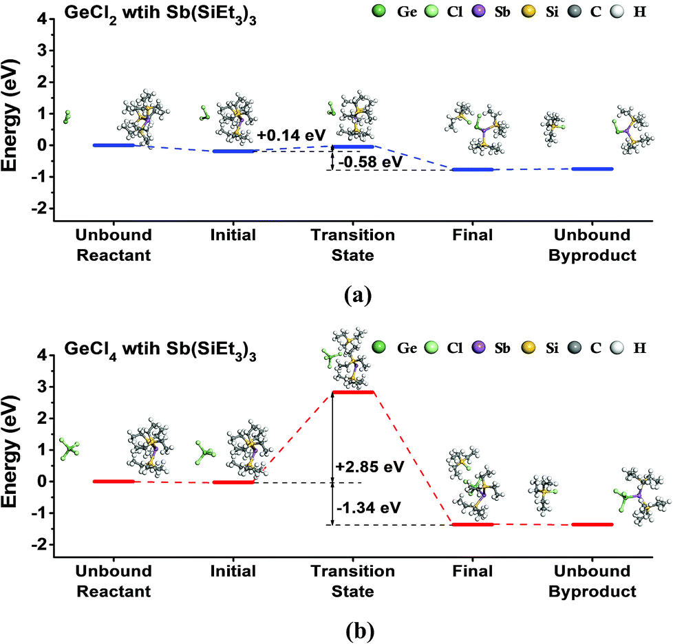 | ||
| Fig. 1 The energy diagram for the ligand-exchange reaction of (a) GeCl2 or (b) GeCl4 with Sb(SiEt3)3, assuming that a chlorine atom of Ge precursor was exchanged by a SiEt3 ligand of Sb(SiEt3)2. Reaction products are ClGeSb(SiEt3)2 and SiEt3Cl for GeCl2, and Cl3GeSb(SiEt3)2 and SiEt3Cl for GeCl4. | ||
The growth kinetic of ALD Ge–Sb film using GeCl2-dioxane and Sb(SiEt3)3 was investigated at 100 °C by QCM measurement. The substrate temperature was set to 100 °C because the precursor pulse time required for saturation of the deposition rate was the shortest in the preliminary work using another reactor (not shown here). The mass changes by 20 pulses of GeCl2-dioxane or Sb(SiEt3)3 was less than 0.01 ng cm−2, which shows the thermal decomposition of the precursors is negligible. Fig. 2 shows the mass change per cycle (ng per cm2 per cycle) as functions of the feeding time of each precursor. Self-limited growth was observed for the Ge precursor pulse longer than 10 s and for the Sb precursor pulse longer than 10 s, respectively. The saturated mass change per cycle was ∼15.6 ng per cm2 per cycle, and the saturated growth rate was 0.021 nm per cycle by TEM observation.
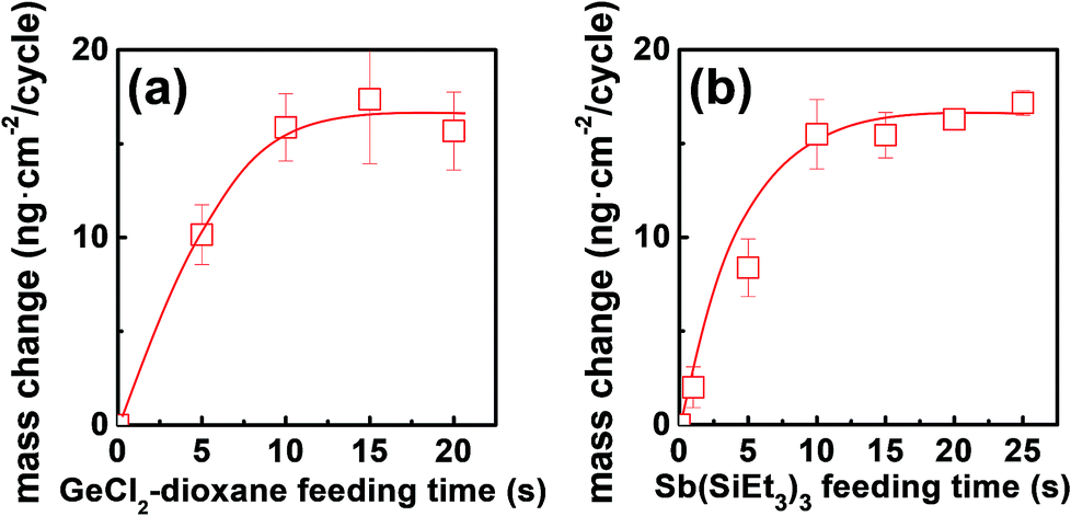 | ||
| Fig. 2 Mass change per cycle of ALD Ge–Sb at 100 °C obtained by QCM measurements as functions of (a) GeCl2-dioxane feeding time and (b) Sb(SiEt3)3 feeding time. The feeding time of Sb(SiEt3)3 was fixed at 15 s in (a), and the feeding time of GeCl2-dioxane was fixed at 10 s in (b). | ||
The composition ratio of Ge to Sb of the ALD Ge–Sb film is approximately 2.2 by AES, as shown in Fig. 3. We investigated the effect of Ge precursor feeding time on the composition, but the composition was almost constant regardless of Ge precursor feeding time. The ALD film contained approximately 10% of carbon impurities, but carbon impurities are not attributed to dioxane or silyl groups of the precursors because no O or Si impurities were not detected in the deposited film. The reaction byproduct of the ALD process of this work is Et3SiCl as described in eqn (1), and Knapas et al. observed the dissociation of Et3SiCl to form Et2SiClH and C2H4 during the ALD of GeTe at 90 °C using the GeCl2-dioxane and Te(SiEt3)2.38 Since C2H4 is known to adsorb well on the surface of Ge,39 Si,40 or metal,41,42 it would be redeposited on the growing film surface, resulting in carbon impurities.
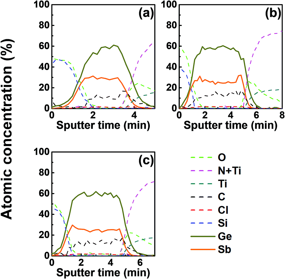 | ||
| Fig. 3 The AES depth profiles of the ALD Ge–Sb film prepared with the Ge precursor feeding times of (a) 5 s, (b) 10 s, and (c) 15 s. The ALD Ge–Sb films were deposited on TiN substrates and were passivated by e-beam evaporated silicon oxide films. | ||
Fig. 4 shows the Raman spectra of the ALD film. The spectrum was almost the same regardless of Ge precursor feeding time. A peak corresponding to Ge–Sb bonds was found at ∼260 cm−1 with a shoulder peak at ∼220 cm−1.43 The peaks at ∼75 cm−1 and 150 cm−1 correspond to amorphous Ge–Ge bonds,44 and the peaks at ∼110 cm−1 and ∼160 cm−1 correspond to Sb–Sb bonds.45
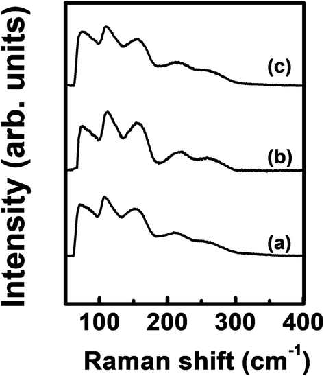 | ||
| Fig. 4 Raman spectra of the ALD Ge–Sb films prepared with the Ge precursor feeding times of (a) 5 s, (b) 10 s, and (c) 15 s. | ||
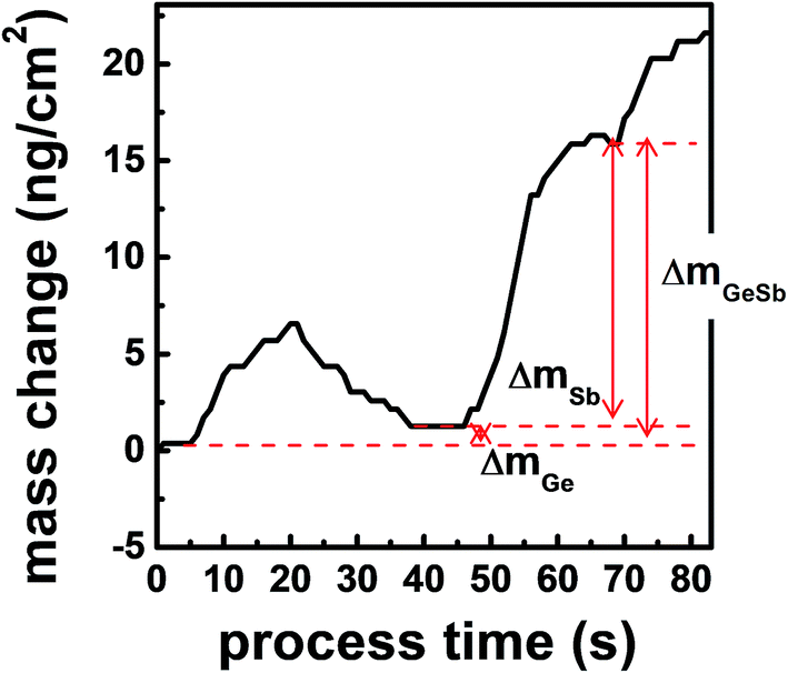
Fig. 5 shows the mass change of the QCM sensor during the ALD process. The QCM analysis gives information about the surface species on the growing film surface because the mass changes by half-reactions are mainly due to the exchange of ligands. The decrement during purge is due to the release of the physisorbed molecules. mGeSb denotes the mass increase after an ALD cycle. mGe and mSb indicate the mass change by the first and the second half-reactions, respectively, and were determined by saturated frequency changes after the purging. During the first half-reaction by GeCl2-dioxane, SiEt3 is removed by forming Et3SiCl, and GeCl is chemisorbed on the surface. In Fig. 5, mGe is very small but is positive. If we assume that the deposited film is Ge3Sb2, the mass change after the first half cycle should be negative because SiEt3 (115.27 u) leaving the surface is heavier than GeCl (108.09 u) adsorbing on the surface. Ge2.2Sb has about 47% more Ge than Ge3Sb2 (Ge1.5Sb), so the mass gain increases by 33.92 u corresponding to 0.47 Ge atoms, resulting in the positive mass change of 26.74 u during the first half-reaction. If dioxane (88.11 u) could be chemisorbed on the surface, mGe should be significantly increased. Therefore, dioxane did not participate in the ALD reaction after being separated from GeCl2-dioxane, confirming the assumption in eqn (1). During the second half reaction by Sb(SiEt3)3, Cl is removed by forming Et3SiCl, and Sb(SiEt3)2 is chemisorbed on the surface. A relatively large mSb is due to the difference in masses of Cl (35.45 u) and Sb(SiEt3)2 (352.30 u). In Fig. 5, the observed value of mGeSb/mGe is 17.4, which is comparable to the calculated value of 14.2 considering that a large error occurs in mGeSb/mGe due to the small error of mGe.
 | ||
| Fig. 5 The mass change during the ALD process using GeCl2 and Sb(SiEt3)3. mGeSb denotes the mass increase after an ALD cycle. mGe and mSb indicate the mass increase by feeding of Ge and Sb precursors, respectively. | ||
Since the Ge(II) precursor and Sb(III) precursor of this study have 2 and 3 ligands, respectively, the ligand-exchanging reaction assumed in Fig. 1 would produce a Ge3Sb2 film. However, the AES composition ratio of Ge to Sb of the ALD Ge–Sb film was approximately 2.2, which is higher than 1.5 of Ge3Sb2. Pore et al.28 also reported a Ge concentration of 82% in the ALD Ge–Sb film, which is even higher than the present study. The most stable oxidation state of Ge is +4, and Ge with the oxidation state of +2 is stabilized by dioxane in the GeCl2-dioxane complex. When GeCl2-dioxane molecules begin to be supplied into the ALD reactor, they initially react with the 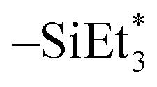 surface groups to form the –GeCl* surface groups and volatile ClSiEt3 and dioxane molecules. Since Ge atoms in –GeCl* groups are not stabilized by dioxane, additional GeCl2-dioxane molecules would have a chance to interact with a portion of Ge atoms in –GeCl* groups, resulting in a Ge–Sb film with a higher Ge concentration than Ge3Sb2, as illustrated in Fig. 6. Further research using in situ surface analyses is needed to reveal the reaction mechanism for high Ge concentrations in the ALD Ge–Sb films.
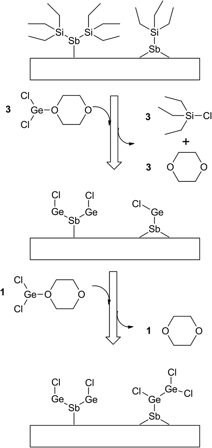 | ||
| Fig. 6 The proposed surface reaction of ALD GeSb from GeCl2-dioxane and Sb(SiEt3)3 to form Ge-rich Ge–Sb films. | ||
B. Tellurization of the ALD Ge–Sb film
We investigated the effect of tellurization annealing temperature on the composition profile of the ALD Ge–Sb film. 11 nm-thick ALD Ge–Sb films were prepared by alternating exposures to GeCl2-dioxane and Sb(SiEt3)3 for 500 cycles and then tellurized for 100 cycles at different temperatures ranging from 170 to 250 °C. The AES depth profiles of the tellurized films are shown in Fig. 7. The ALD Ge–Sb films turned into tellurium-containing films by the tellurization annealing. When the tellurization temperature was 180 °C or below, tellurium was distributed only near the surface. When annealed at 190 °C, tellurium atoms diffused into the lower part of the Ge–Sb film, but tellurium concentration was not uniform. When annealed at 230 °C or higher temperatures, the entire film was fully tellurized to form a GST film having a composition similar to Ge3Sb2Te6. Since the GST composition with the highest Ge content is Ge2Sb2Te5, the Ge3Sb2Te6 phase would be the mixture of Ge2Sb2Te5 and GeTe. The tellurized films have lower [Ge]/[Sb] ratios than ∼2.2 of the as-deposited ALD film because Ge diffuses into the TiN underlayer as well as the silicon oxide overlayer. The concentration of carbon impurities in the as-deposited ALD Ge–Sb film were eliminated by tellurization annealing at 230 °C or higher temperatures because the desorption of the chemisorbed C2H4 molecules become active at high substrate temperatures.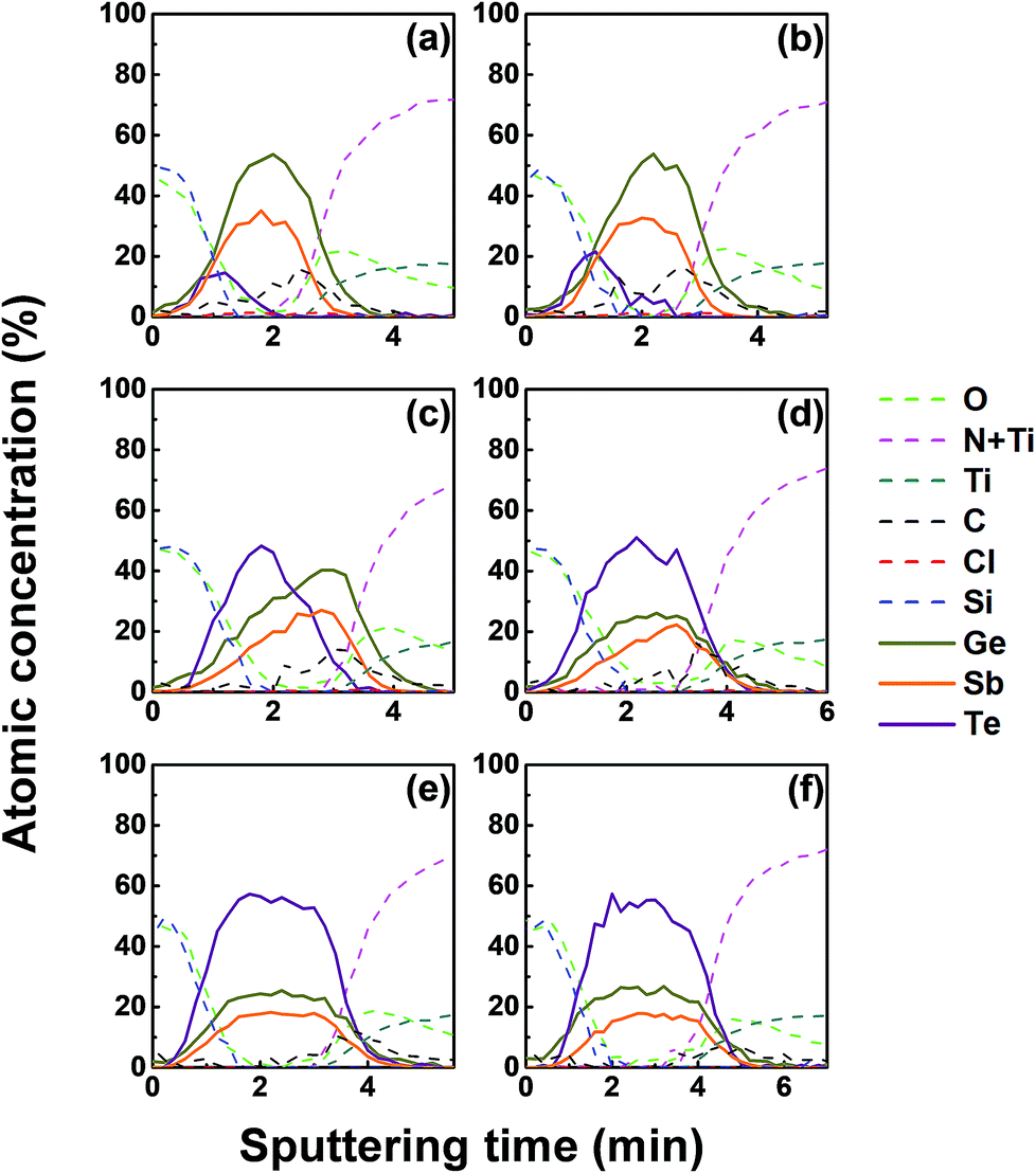 | ||
| Fig. 7 AES depth profile of the ALD Ge–Sb film on a TiN substrate after tellurization annealing for 100 cycles at different temperatures: (a) 170 °C, (b) 180 °C, (c) 190 °C, (d) 200 °C, (e) 230 °C, and (f) 250 °C. Immediately after unloading the tellurized film from the reactor, a 4 nm thick silicon oxide film was deposited on the tellurized film using an e-beam evaporator. | ||
Fig. 8 shows the concentration ratio of Ge to Sb ([Ge]/[Sb]) of the ALD Ge–Sb film before and after tellurization. The central region with low oxygen concentration corresponds to ALD Ge–Sb film while the regions with high oxygen concentrations correspond to the silicon oxide overlayer (left) and the TiN underlayer (right). The [Ge]/[Sb] ratio is high in the TiN and the silicon oxide layers in all cases, suggesting that Ge diffuses into TiN and silicon oxide. Fig. 8(a) shows that the [Ge]/[Sb] is the lowest at the Ge–Sb/TiN and SiOx/Ge–Sb interface. The nonuniform distribution of [Ge]/[Sb] is because the diffusion of Ge into TiN and SiOx occurred, but the redistribution of Ge in the Ge–Sb film was very slow. At higher annealing temperature shown in Fig. 8(d), the Ge was redistributed in the GST film, resulting in a relatively uniform [Ge]/[Sb] ratio. Therefore, as the annealing temperature increases, the redistribution of Ge in GST film is more active, increasing the minimum [Ge]/[Sb] value. The total amount of Ge in GST film can be determined by the average [Ge]/[Sb] value, which decreases with increasing annealing temperature. As a consequence, the [Ge]/[Sb] of the as-deposited Ge–Sb film is about 2.2 as shown in Fig. 8(a) but decreased to about 1.5 by tellurization at 230 °C as shown in Fig. 8(d).
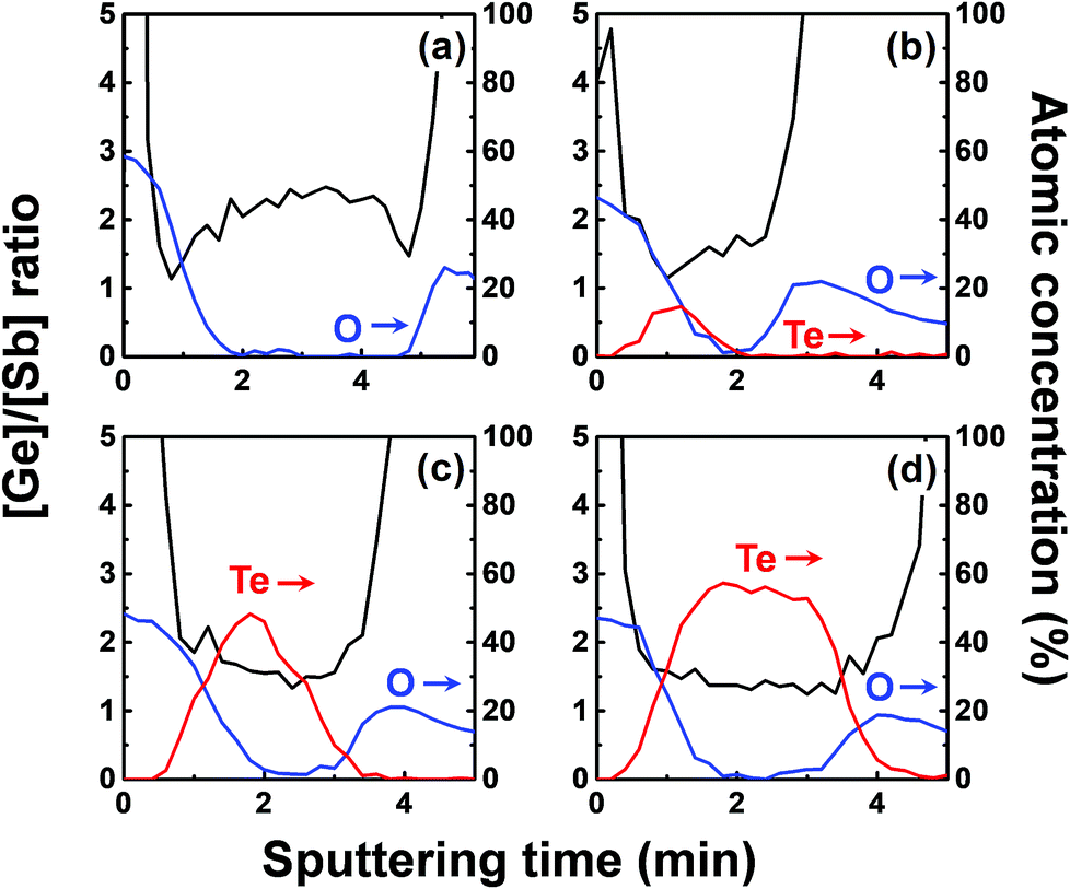 | ||
| Fig. 8 The ratio of germanium to antimony and the concentration of tellurium and oxygen in the ALD Ge–Sb film: (a) before tellurization; after tellurization at (b) 170 °C, (c) 190 °C, and (d) 230 °C. Immediately after unloading the tellurized film from the reactor, a 4 nm thick silicon oxide film was deposited on the tellurized film using an e-beam evaporator. | ||
Since the diffusion of Ge into TiN is observed before the tellurization annealing, Ge diffuses even during the ALD at 100 °C. Also, Ge was incorporated in the silicon oxide passivation layer during the e-beam evaporation. The report on the diffusion into TiN was rare, and the active diffusion of Ge into TiN might be due to the columnar structure of sputtered TiN.46 To improve the reliability of the PCRAM device, ALD GST films, as well as sputtered GST films, require a diffusion barrier superior to TiN as the electrode material. The diffusion of Ge in silicon oxide at high temperatures has been reported,47 and the active diffusion of Ge into the e-beam evaporated silicon oxide layer at low temperatures might also be due to the columnar structure of the silicon oxide film.48
The structural changes by tellurization at different annealing temperatures were investigated by Raman spectroscopy, as shown in Fig. 9. At the tellurization temperature of 180 °C or below, the Raman spectra show little changes from the spectrum before tellurization. Peaks corresponding to Ge–Sb bonds,43 amorphous Ge–Ge bonds,44 and an Sb–Sb bond,45 described in Fig. 4, still exist. However, when the annealing temperature was raised to 190 °C or higher temperatures, the Ge–Sb bond peaks disappeared at ∼220 and ∼260 cm−1, which agrees with AES depth profiles in Fig. 7. The intensities of amorphous Ge–Ge bond peaks at ∼75 and ∼150 cm−1 also decreased with increasing tellurization temperature and are overlapped with an Sb–Te peak evolving at ∼70 cm−1 and an Sb–Sb peak remaining at ∼160 cm−1.45,49 The change of an Sb–Sb peak at ∼110 cm−1 was hard to distinguish with the vibration of heteropolar bond in the tetrahedral GeTe4 and pyramidal SbTe3 evolving at almost the same wave number.50 When the tellurization annealing temperature is 230 °C or above, an Sb–Sb peak at ∼160 cm−1 disappeared, and peaks corresponding to Sb–Te and Ge–Te bonds strongly evolved. The intensity of the peak at ∼110 cm−1 significantly increased, Sb–Te peaks evolved at ∼70 cm−1 and ∼175 cm−1, and a weak peak corresponding to Ge–Te bonds evolved at ∼125 cm−1.51 The Sb–Te bond peak located at ∼175 cm−1 suggests that the crystal structure of the tellurized film was hexagonal close-packing (HCP).52,53
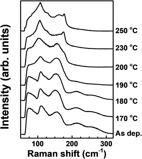 | ||
| Fig. 9 Raman spectra of the ALD Ge–Sb films before and after the tellurization at different temperatures. | ||
The phase transition temperature of the tellurized Ge–Sb film was investigated as shown in Fig. 10. The temperature at which the resistance rapidly drops was determined as the phase transition temperature. Since the film was crystallized by tellurization annealing, the annealed film was amorphized by melt-quenching with a KrF excimer laser. Since the crystallization temperature of GeSb is higher than 300 °C,54 we could not observe the phase transition of the ALD Ge–Sb thin film annealed at low temperature or as-deposited state even when the sample was heated up to 300 °C, the maximum temperature of the probe station that we used. For the films fully tellurized at 200 °C or higher temperatures, the phase transition temperature was ∼123 °C, which is similar to ∼130 °C of the Ge2Sb2Te5 prepared by sputtering.55
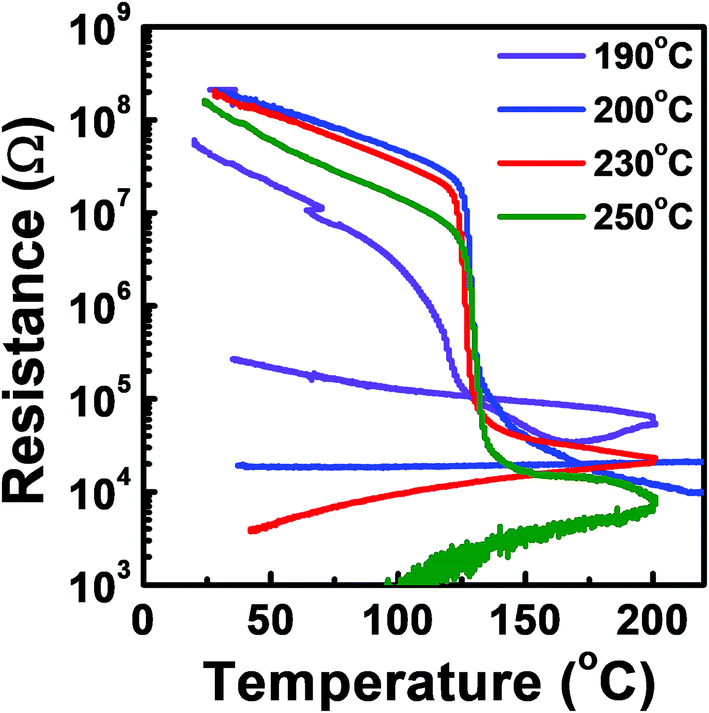 | ||
| Fig. 10 Resistance versus temperature plot of the ALD Ge–Sb film tellurized at different temperatures. | ||
The gap filling characteristics of the tellurized ALD Ge–Sb film were investigated by TEM, as shown in Fig. 11. An 11 nm-thick ALD Ge–Sb film was prepared on the trench pattern with an aspect ratio of 3.75 and a top opening width of 40 nm. As the tellurization temperature increases, the tellurium concentration increased, and the volume of the conformal ALD film tends to expand. In particular, when tellurized at 230 °C, the trench pattern is completely filled with the tellurized film and the 11 nm of GeSb thin film deposited on the planar substrate turned into 24 nm of GeSbTe film. The EDS mapping shows the uniform distribution of Te in the trench. However, when the film was tellurized at 250 °C, a void was formed at the bottom of the pattern, probably due to severe agglomeration of the film.
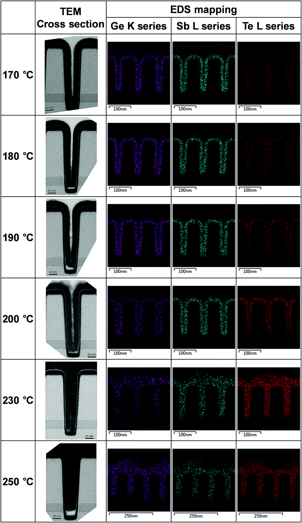 | ||
| Fig. 11 Cross-sectional TEM photographs and EDS mapping of the tellurized ALD Ge–Sb film prepared on a trench pattern. | ||
Conclusions
We prepared ALD Ge–Sb film by alternating exposures to GeCl2-dioxane and Sb(SiEt3)3 precursors at 100 °C. The growth rate was 0.021 nm per cycle, and the composition ratio of Ge to Sb was approximately 2.2. The ALD Ge–Sb films turned into GST films by the tellurization annealing. When the tellurization temperature was raised to 190 °C or higher temperatures, the Ge–Sb bond peaks and the amorphous Ge–Ge bond peak disappeared. The peaks corresponding to Ge–Te and Sb–Te bonds were evolved at 200 °C or higher temperatures, resulting in the phase transition temperature of 123 °C. At 230 °C or higher temperatures, the entire film was fully tellurized to form a crystalline GST film having a relatively uniform composition of Ge3Sb2Te6, and the carbon impurities in the as-deposited ALD Ge–Sb film were eliminated. As the tellurization temperature increases, the volume of the ALD film is expanded owing to the incorporation of tellurium, resulting in complete filling of a trench pattern by GST film after the tellurization at 230 °C. Also, the thin tellurized film showed excellent step coverage with a smooth surface.Conflicts of interest
There are no conflicts to declare.Acknowledgements
This research was supported by the MOTIE (Ministry of Trade, Industry & Energy) (project number 10045360 and 10080625) and KSRC (Korea Semiconductor Research Consortium) support program for the development of the future semiconductor device.References
- G. Yue-Feng, L. Yun, S. Zhi-Tang and F. Song-Lin, Chin. Phys. Lett., 2008, 25, 3455–3458 CrossRef.
- G. W. Burr, B. N. Kurdi, J. C. Scott, C. H. Lam, K. Gopalakrishnan and R. S. Shenoy, IBM J. Res. Dev., 2008, 52, 449–464 Search PubMed.
- J. Meena, S. Sze, U. Chand and T.-Y. Tseng, Nanoscale Res. Lett., 2014, 9, 526 CrossRef PubMed.
- S. Hudgens and B. Johnson, MRS Bull., 2004, 29, 829–832 CrossRef CAS.
- D. H. Im, J. I. Lee, S. L. Cho, H. G. An, D. H. Kim, I. S. Kim, H. Park, D. H. Ahn, H. Horii, S. O. Park, U. I. Chung and J. T. Moon, in 2008 IEEE International Electron Devices Meeting, IEEE, 2008, pp. 1–4 Search PubMed.
- M. Kinoshita, Y. Sasago, H. Minemura, Y. Anzai, M. Tai, Y. Fujisaki, S. Kusaba, T. Morimoto, T. Takahama, T. Mine, A. Shima, Y. Yonamoto and T. Kobayashi, in 2012 Symposium on VLSI Technology (VLSIT), IEEE, 2012, vol. 97, pp. 35–36 Search PubMed.
- N. Yamada, E. Ohno, K. Nishiuchi, N. Akahira and M. Takao, J. Appl. Phys., 1991, 69, 2849–2856 CrossRef CAS.
- N. Yamada, in 1997 Optical Data Storage Topical Meeting ODS Conference Digest, ed. H. Birecki and J. Z. Kwiecien, IEEE, 1997, vol. 3109, pp. 98–99 Search PubMed.
- T. Ohta, J. Optoelectron. Adv. Mater., 2001, 3, 609–626 CAS.
- C.-F. Chen, A. Schrott, M. H. Lee, S. Raoux, Y. H. Shih, M. Breitwisch, F. H. Baumann, E. K. Lai, T. M. Shaw, P. Flaitz, R. Cheek, E. A. Joseph, S. H. Chen, B. Rajendran, H. L. Lung and C. Lam, in 2009 IEEE International Memory Workshop, IEEE, 2009, pp. 1–2 Search PubMed.
- H. K. Lyeo, D. G. Cahill, B. S. Lee, J. R. Abelson, M. H. Kwon, K. B. Kim, S. G. Bishop and B. K. Cheong, Appl. Phys. Lett., 2006, 89, 151904 CrossRef.
- M. H. Jang, S. J. Park, S. J. Park, M.-H. Cho, E. Z. Kurmaev, L. D. Finkelstein and G. S. Chang, Appl. Phys. Lett., 2010, 97, 152113 CrossRef.
- S. W. Ryu, J. H. Oh, J. H. Lee, B. J. Choi, W. Kim, S. K. Hong, C. S. Hwang and H. J. Kim, Appl. Phys. Lett., 2008, 92, 142110 CrossRef.
- M. Bouška, S. Pechev, Q. Simon, R. Boidin, V. Nazabal, J. Gutwirth, E. Baudet and P. Němec, Sci. Rep., 2016, 6, 26552 CrossRef PubMed.
- B. J. Choi, S. Choi, Y. C. Shin, K. M. Kim, C. S. Hwang, Y. J. Kim, Y. J. Son and S. K. Hong, Chem. Mater., 2007, 19, 4387–4389 CrossRef CAS.
- J. Lee, S. Choi, C. Lee, Y. Kang and D. Kim, Appl. Surf. Sci., 2007, 253, 3969–3976 CrossRef CAS.
- V. Pore, T. Hatanpää, M. Ritala and M. Leskela, J. Am. Chem. Soc., 2009, 131, 3478–3480 CrossRef CAS PubMed.
- M. Ritala, V. Pore, T. Hatanpää, M. Heikkilä, M. Leskelä, K. Mizohata, A. Schrott, S. Raoux and S. M. Rossnagel, Microelectron. Eng., 2009, 86, 1946–1949 CrossRef CAS.
- M. Leskelä, V. Pore, T. Hatanpää, M. Heikkilä, M. Ritala, A. Schrott, S. Raoux and S. Rossnagel, ECS Trans., 2009, 25, 399–407 Search PubMed.
- T. Eom, T. Gwon, S. Yoo, B. J. Choi, M.-S. Kim, I. Buchanan, S. Ivanov, M. Xiao and C. S. Hwang, Chem. Mater., 2015, 27, 3707–3713 CrossRef CAS.
- H. K. Kim, in SEMICON Korea, 2016 Search PubMed.
- K. Do, D. Lee, D.-H. Ko, H. Sohn and M.-H. Cho, Electrochem. Solid-State Lett., 2010, 13, H284 CrossRef CAS.
- H. K. Kim, S. J. Chae and B. K. Lee, in E*Pcos 2015, 2015 Search PubMed.
- S. A. Gamboa, P. J. Sebastian and M. A. Rivera, Sol. Energy Mater. Sol. Cells, 1998, 52, 293–299 CrossRef CAS.
- S. A. Gamboa, P. J. Sebastian, X. Mathew, H. Nguyen-Cong and P. Chartier, Sol. Energy Mater. Sol. Cells, 1999, 59, 115–124 CrossRef.
- Z. Sun, S. Liufu, X. Chen and L. Chen, J. Phys. Chem. C, 2011, 115, 16167–16171 CrossRef CAS.
- K. Suda, T. Uno, T. Miyakawa, N. Sawamoto, H. Machida, M. Ishikawa, H. Sudoh, Y. Ohshita and A. Ogura, Jpn. J. Appl. Phys., 2013, 52, 128006 CrossRef.
- V. Pore, K. Knapas, T. Hatanpää, T. Sarnet, M. Kemell, M. Ritala, M. Leskelä and K. Mizohata, Chem. Mater., 2011, 23, 247–254 CrossRef CAS.
- B. Han, Y. Kim, Y.-J. Kim, M.-H. Cho, S.-K. Rha and W.-J. Lee, ECS J. Solid State Sci. Technol., 2019, 8, P298–P302 CrossRef.
- Elsevier, Mater. Sci. Semicond. Process., 2015, 40, 50–57 CrossRef.
- J.-F. Zheng, US Pat. 8,617.972 B2, Westport, CT, US, 2013.
- J. P. Perdew, K. Burke and M. Ernzerhof, Phys. Rev. Lett., 1996, 77, 3865–3868 CrossRef CAS PubMed.
- B. Delley, J. Chem. Phys., 1990, 92, 508–517 CrossRef CAS.
- B. Han, Y.-J. Kim, J.-M. Park, L. L. Yusup, J. Shin and W.-J. Lee, J. Nanosci. Nanotechnol., 2017, 17, 3472–3476 CrossRef CAS.
- B. Han, Y.-J. Kim, J.-M. Park, L. L. Yusup, H. Ishii, C. Lansalot-Matras and W.-J. Lee, J. Nanosci. Nanotechnol., 2016, 16, 4924–4928 CrossRef CAS PubMed.
- B. Han, K. Ha Choi, J. Min Park, J. Woo Park, J. Jung and W.-J. Lee, J. Vac. Sci. Technol., A, 2013, 31, 01A145 CrossRef.
- J. M. Park, S. J. Jang, L. L. Yusup, W. J. Lee and S. I. Lee, ACS Appl. Mater. Interfaces, 2016, 8, 20865–20871 CrossRef CAS PubMed.
- K. Knapas, T. Hatanpaa, M. Ritala and M. Leskela, Chem. Mater., 2010, 22, 1386–1391 CrossRef CAS.
- P. Lal, A. V. Teplyakov, Y. Noah, M. J. Kong, G. T. Wang and S. F. Bent, J. Chem. Phys., 1999, 110, 10545–10553 CrossRef CAS.
- L. Clemen, R. M. Wallace, P. A. Taylor, M. J. Dresser, W. J. Choyke, W. H. Weinberg and J. T. Yates, Surf. Sci., 1992, 268, 205–216 CrossRef CAS.
- F. P. Netzer and R. A. Wille, Surf. Sci., 1978, 74, 547–567 CrossRef CAS.
- E. W. R. Steacie and H. V. Stovel, J. Chem. Phys., 1934, 2, 581–584 CrossRef CAS.
- C. C. Huang, B. Gholipour, K. Knight, J. Y. Ou and D. W. Hewak, Adv. OptoElectron., 2012, 2012, 1–7 CrossRef.
- P. Kazimierski, J. Tyczkowski, M. Kozanecki, Y. Hatanaka and T. Aoki, Chem. Mater., 2002, 14, 4694–4701 CrossRef CAS.
- P. Němec, V. Nazabal, A. Moreac, J. Gutwirth, L. Beneš and M. Frumar, Mater. Chem. Phys., 2012, 136, 935–941 CrossRef.
- S. K. Rha, W. J. Lee, S. Y. Lee, Y. S. Hwang, Y. J. Lee, D. Il Kim, D. W. Kim, S. S. Chun and C. O. Park, Thin Solid Films, 1998, 320, 134–140 CrossRef CAS.
- M. Ogino, Y. Oana and M. Watanabe, Phys. Status Solidi, 1982, 72, 535–541 CrossRef CAS.
- A. Barna, O. Geszti, L. Gosztola and E. Seyfried, MRS Proc., 1985, 61, 367 CrossRef.
- K. M. F. Shahil, M. Z. Hossain, V. Goyal and A. A. Balandin, J. Appl. Phys., 2012, 111, 054305 CrossRef.
- L. Bo, S. Zhi-Tang, Z. Ting, F. Song-Lin and C. Bomy, Chin. Phys., 2004, 13, 1947–1950 CrossRef.
- K. S. Andrikopoulos, S. N. Yannopoulos, G. A. Voyiatzis, A. V. Kolobov, M. Ribes and J. Tominaga, J. Phys.: Condens. Matter, 2006, 18, 965–979 CrossRef CAS.
- E. M. Vinod, K. Ramesh, R. Ganesan and K. S. Sangunni, Appl. Phys. Lett., 2014, 104, 063505 CrossRef.
- G. C. Sosso, S. Caravati, C. Gatti, S. Assoni and M. Bernasconi, J. Phys.: Condens. Matter, 2009, 21, 245401 CrossRef CAS PubMed.
- S. Raoux, H.-Y. Cheng, B. Muñoz and J. L. Jordan-Sweet, Eur. Phase Chang. Ovonic Sci. Symp., 2009, pp. 91–98 Search PubMed.
- T. Nirschl, J. B. Philipp, T. D. Happ, G. W. Burr, B. Rajendran, M.-H. Lee, A. Schrott, M. Yang, M. Breitwisch, C.-F. Chen, E. Joseph, M. Lamorey, R. Cheek, S.-H. Chen, S. Zaidi, S. Raoux, Y. C. Chen, Y. Zhu, R. Bergmann, H.-L. Lung and C. Lam, in 2007 IEEE International Electron Devices Meeting, IEEE, 2007, pp. 461–464 Search PubMed.
| This journal is © The Royal Society of Chemistry 2019 |