
 Open Access Article
 This Open Access Article is licensed under a Creative Commons Attribution-Non Commercial 3.0 Unported Licence
Evaluation of dual layered photoanode for enhancement of visible-light-driven applications†
Suhee Kang a,
Joonyoung Janga,
Hyo-Joon Kima,
Sung-Hoon Ahnb and
Caroline Sunyong Lee*a
a,
Joonyoung Janga,
Hyo-Joon Kima,
Sung-Hoon Ahnb and
Caroline Sunyong Lee*a
aDepartment of Materials and Chemical Engineering, Hanyang University, South Korea. E-mail: sunyonglee@hanyang.ac.kr
bDepartment of Mechanical and Aerospace Engineering, Seoul National University, South Korea
First published on 31st May 2019
Abstract
Ternary structures consisting of hollow g-C3N4 nanofibers/MoS2/sulfur, nitrogen-doped graphene and bulk g-C3N4 (TCN) were designed as a dual layered film and fabricated using a spin-coating method. The first ternary structures were spin-coated on fluorine-doped tin oxide (FTO) glass, followed by spin-coating of g-C3N4 film to form dual layers. We characterized the microstructural morphologies, chemical composition/bonding and optical properties of the dual layered film and observed significantly reduced recombination rates of photo-induced electron–hole pairs due to effective separation of the charge carriers. We tested methylene blue (MB) photodegradation and observed remarkable MB degradation by the dual layered film over 5 hours, with a kinetic rate constant of 1.24 × 10⁻³ min−1, which is about four times faster than that of bare TCN film. Furthermore, we estimated the H2 evolution of the dual layered film to be 44.9 μmol over 5 hours, and carried out stable recycling over 45 hours under visible irradiation. Due to the lower electrochemical impedance spectroscopy (EIS) resistance value of the dual layered film (∼50 ohm cm2) compared to the TCN film, the ternary structures and bulk g-C3N4 film were well-connected as a heterojunction, reducing the resistance at the interface between the film and the electrolyte. These results indicate that the effective separation of the photo-induced electron–hole pairs using the dual layered film dramatically improved its photo-response ability under visible light irradiation.
1. Introduction
Photoactive materials have been studied for a wide range of applications, motivated by severe environmental issues such as global warming, fine dust, and water pollution.1–3 Historically, photoactive materials have been identified based on Honda and Fujishima's 1972 photoelectrochemical (PEC) water splitting report, on TiO2 electrodes.4 That study sparked much research over the last 40 years in various fields, including on purification of water containing organic pollutants, H2 evolution activity, and PEC water splitting under sunlight. Many researchers have studied TiO2 for applications to photocatalytic performance.5–9 For example, Xiang et al. reported that a TiO2 nanocrystal with layered MoS2/graphene hybrid was synthesized to enhance H2 evolution efficiency under ultraviolet (UV) light.10 Priebe et al. reported that as-prepared Au–TiO2 catalysts showed higher H2 evolution rates under ultraviolet-visible (UV-VIS) irradiation when the deposition–precipitation method was applied during the synthesis.11 Nevertheless, photocatalysts, which have wide band gap energies, can only be used in the UV spectrum, which represents less than 5% of the solar spectrum.12,13 Thus, band gap engineering is necessary to enhance the efficiency of photocatalytic activity within the specific range of the solar spectrum.To utilize the visible band spectrum, other photoactive materials or hetero-combinations could be considered for lab-scale studies and future commercialization. In our previous study, one-dimensional hollow graphitic carbon nitride (g-C3N4), molybdenum disulfide (MoS2) and sulfur/nitrogen co-doped graphene (SNG) were synthesized to respond only in the visible range via a one-pot hydrothermal method at a relatively low temperature. g-C3N4 is a metal-free polymeric semiconductor consisting of earth-abundant elements of carbon/nitrogen, and is thus environmentally benign.14 The layered structures of MoS2-exposed sulfur atoms on Mo edges exhibit good stability, even in strong acids, as well as outstanding physical, optical and electrical properties.15,16 Sheet-like structures of graphene are well-known to possess two-dimensional sp2-hybridized carbon structures with high surface areas, high electrical conductivity, and good chemical stability,17–19 especially in the presence of defects due to sulfur or nitrogen doping.20,21 MoS2 and g-C3N4 are used to reduce electrons and oxidize holes, respectively, because their electronic properties well match their conduction and valence bands,.22 Moreover, SNG has also been used to enlarge active sites, thus accelerating charge transport.23 Despite these suitable materials, bulk type catalyst powders still have serious problems because they agglomerate in aqueous solution, resulting in rapid recombination rates of photo-induced charge carriers.24,25 Moreover, a particulate form of photocatalysts tend to decrease the photocatalytic efficiency due to light scattering or charge recombination.26 To overcome this, as-synthesized powders were prepared as a photoanode film using a simple spin-coating method, thus improving their photocatalytic activity.
In this study, we spin-coated a dual layered photoanode film using a ternary structure of hollow g-C3N4 nanofibers (HGCNF)/SNG/MoS2 followed by bulk g-C3N4 from thiourea precursors (denoted as TCN) for photo-responsive applications. The ternary structures were first spin-coated onto FTO substrates and the bulk g-C3N4 was then spin-coated onto ternary structures. Finally, we obtained the dual layered film and demonstrated its increased absorption under the visible spectrum; we also reduced its band gap energy compared to that of bare TCN film. To confirm the photo-responsivity of the film, we carried out photocatalytic activities, organic pollutant degradation on methylene blue (MB) and H2 evolution, using the as-prepared photoanode films, namely the TCN and dual layered film, under visible light irradiation. The dual layered film achieved faster pollutant removal, as well as higher H2 production, due to its heterojunctions of ternary structures and TCN, and is thus suitable for various photo-responsive applications.
2. Experimental section
2.1 Materials
To supply sulfide from molybdenum sulfide, SNG, and bulk g-C3N4, thiourea was purchased from Wako (Japan). Sodium molybdate (NaMoO4) was purchased from Sigma-Aldrich (Germany). Sodium sulfate (Na2SO4) and triethanolamine (TEOA) were purchased from SAM-CHUN (Korea). H2PtCl2 was purchased from Sigma-Aldrich (USA) for H2 evolution reactions. A conductive fluorine-doped tin oxide (FTO, 15 mΩ) substrate was used as the photoanode film. Liquion solution was purchased from Ion Power (USA) to be mixed with powder for spin-coating. All chemicals were used directly without any further purification.2.2 Preparation of catalysts of ternary structures and bulk g-C3N4
To prepare the ternary structure of HGCNF/SNG/MoS2, we followed the synthesis procedure used in our previous study.27 Briefly, 0.1 g of HGCNF were sonicated using an ultra-high sonicator for 30 min in GO solution/distilled water (4![[thin space (1/6-em)]](https://www.rsc.org/images/entities/char_2009.gif) :96 v/v%). Afterwards, the dispersion solution was stirred with 0.4 g of Na2MoO4 precursor for 1 hour. Then, 0.8 g of thiourea precursor was added to the solution until it had dissolved completely. After dissolving, a hydrothermal process was carried out under the same conditions. Due to the SNG, the obtained product was freeze-dried after filtration with distilled water and ethanol. Furthermore, the thiourea precursor was used for sintering in a covered crucible at a temperature of up to 520 °C for 2 hours (5 °C min−1) to produce bulk g-C3N4. Finally, we fabricated as-prepared black-colored HGCNF/SNG/MoS2, which we called ternary structures, while the as-prepared yellow-colored bulk g-C3N4 was called TCN.
:96 v/v%). Afterwards, the dispersion solution was stirred with 0.4 g of Na2MoO4 precursor for 1 hour. Then, 0.8 g of thiourea precursor was added to the solution until it had dissolved completely. After dissolving, a hydrothermal process was carried out under the same conditions. Due to the SNG, the obtained product was freeze-dried after filtration with distilled water and ethanol. Furthermore, the thiourea precursor was used for sintering in a covered crucible at a temperature of up to 520 °C for 2 hours (5 °C min−1) to produce bulk g-C3N4. Finally, we fabricated as-prepared black-colored HGCNF/SNG/MoS2, which we called ternary structures, while the as-prepared yellow-colored bulk g-C3N4 was called TCN.
2.3 Fabrication of photoanode films
To fabricate the dual layered photoanode film using these catalysts, 0.2 g of ternary structure powder and TCN powder were prepared separately in 2 mL of Liquion solution until dissolved completely. Then, 0.5 mL of as-prepared ternary structure solution was spin-coated on FTO glass (2 cm × 5 cm) at 2500 rpm for 60 s. and dried in an oven for 2 hours. After drying the film, 0.5 mL of TCN solution was dropped onto the as-fabricated ternary structure under the same spin-coating conditions and dried in the oven for 2 hours. Finally, the fabricated photoanode film was sintered at 150 °C for 1 hour under ambient atmosphere to remove the solvent, after which we stabilized the film. For the comparison, each ternary structure and TCN solution was separately spin-coated on the FTO substrate using the same procedure described above.2.4 Characterization
We differentiated the well-constructed morphologies of the photoanode film using field-emission scanning electron microscopy (FE-SEM; model S4800, Hitachi, Japan), focused ion beam (FIB; model FB-2100, Hitachi, Japan) and transmission electron microscopy (TEM; model JEM-2100F, JEOL, Japan). To observe the crystalline structure and its properties, X-ray diffraction (XRD) using a Cu Kα source (model D/Max-2500/PC; Rigaku/USA Inc., USA) analysis was carried out on the MoS2 and g-C3N4 phases. Fourier transform infrared spectroscopy (FT-IR; model iS10; Thermo Fisher Scientific, UK) and X-ray photoelectron spectroscopy (XPS) using an Al Kα source (Sigma Probe; Thermo Fisher Scientific, UK) were used to confirm the formation of g-C3N4. Then, UV-VIS spectroscopy (model V650; JASCO, Japan) was used to observe the optical absorbance of the films so that we could calculate their band gap energy. Photoluminescence (PL; SC-100; Dongwoo, Korea) was employed to monitor the recombination rate of the as-prepared films at 325 nm laser excitation. All photocatalytic performance tests of transient photocurrents, Mott–Schottky analysis and electrochemical impedance spectroscopy (EIS) were carried out using a potentiostat (VersaSTAT 4; Princeton Applied Research, USA). The photocatalytic degradation solutions were measured by UV-VIS spectroscopy.2.5 Photocatalytic performance
Three different photocatalytic experiments were carried out using the photoanode films. The PEC measurements of the transient photocurrent and EIS proceeded under a three-electrode quartz system with a VersaSTAT 4 potentiostat (Princeton Applied Research) in 0.5 M Na2SO4. The transient photocurrent was applied at 1 V of bias potential versus an Ag/AgCl reference electrode, while chopping the illumination to study the response of the sample to light. The flat band potential was measured at a potential range of −0.5 to 1 V vs. Ag/AgCl with selected frequencies and an amplitude of 10 mV in 0.5 M Na2SO4. The electrochemical impedance was measured at a frequency of 105 to 0.1 Hz with an alternating current (AC) amplitude of 20 mV (biased at 1 V). We used MB pollutant to observe the organic pollutant removal properties of the samples. Before starting the experiment, 0.02 mM of MB solution was prepared with distilled water. Then, 90 mL of MB solution was added to a 100 mL Pyrex glass beaker and the photoanode film was clipped with a tweezer to irradiate its surface. After initiating the irradiation, 3 mL of solution was collected every hour until the degradation was complete. For the active species, the scavenger test was carried out to study photocatalytic mechanism. Before starting the degradation, each scavenger of EDTA (1 mM), t-BuOH (1 mM) and saturated N2 was added into MB solution. After stirring the solution, the photocatalytic activity was proceeded under same condition. We used a 100 mL Pyrex glass beaker in the same way to investigate the H2 evolution of photoanode films. Then, 25 vol% of trimethylamine (TEOA) in 60 mL of aqueous solution was added as a hole scavenger. To enhance its properties, we photo-deposited 1 wt% of platinum (Pt) on the photoanode film with UV irradiation for 5 min. Prior to the reaction, the reactor was sealed with a septum and N2 gas was purged into an aqueous solution to remove oxygen (O2) from the solution. After that, argon (Ar) gas was purged into the reactor to completely eliminate the air. The produced gas was detected using a pulsed discharge detector (PDD) equipped with gas chromatography (GC; model 6500GC; YL Instruments, Korea) and helium gas was employed as a carrier gas. To assess the photocatalytic performance, a 300 W Xe-arc lamp (model 66984; Newport, USA) was used with a UV cut-off filter (>400 nm). The stability test was repeated nine times under the same conditions.3. Results and discussions
3.1 Morphology and characterization of photoanode films
Fig. 1(a)–(c) show SEM images of the surface morphology of the ternary structures, TCN and dual layered films. The ternary structures were well spin-coated on the FTO substrate with its fabricated composites (HGCNF, MoS2 and SNG), while TCN film was spin-coated onto FTO glass with only bulk g-C3N4 structures. When the TCN was coated on the ternary structures, the TCN was entirely wrapped around the ternary structures and partial HGCNFs were observed, as shown in the top view. Fig. 1(d)–(f) show cross-sectional images of the FTO substrate, which we used to assess the coating thickness. The ternary structures and TCN had thicknesses of 3.99 and 2.34 μm, respectively. In the case of the dual layered film, the blue dotted line shows the separation between the TCN, ternary structures and FTO. TCN was coated onto the ternary structures along the dotted curve, indicating its total thickness to be 4.17 μm, while the ternary structures are shown between the dotted line of the ternary structures to the dotted curve of the TCN. Furthermore, the cross-sectional TEM image of dual layered film was observed to confirm that heterojunction between ternary structures and bulk g-C3N4 was well-connected as shown in Fig. S1.† Fig. S1† indicated that the ternary structures with TCN on the FTO glass, formed a well-connected heterojunction. According to the microstructures of these films, the dual layered film demonstrated good formation of ternary structures with bulk g-C3N4 structures (TCN).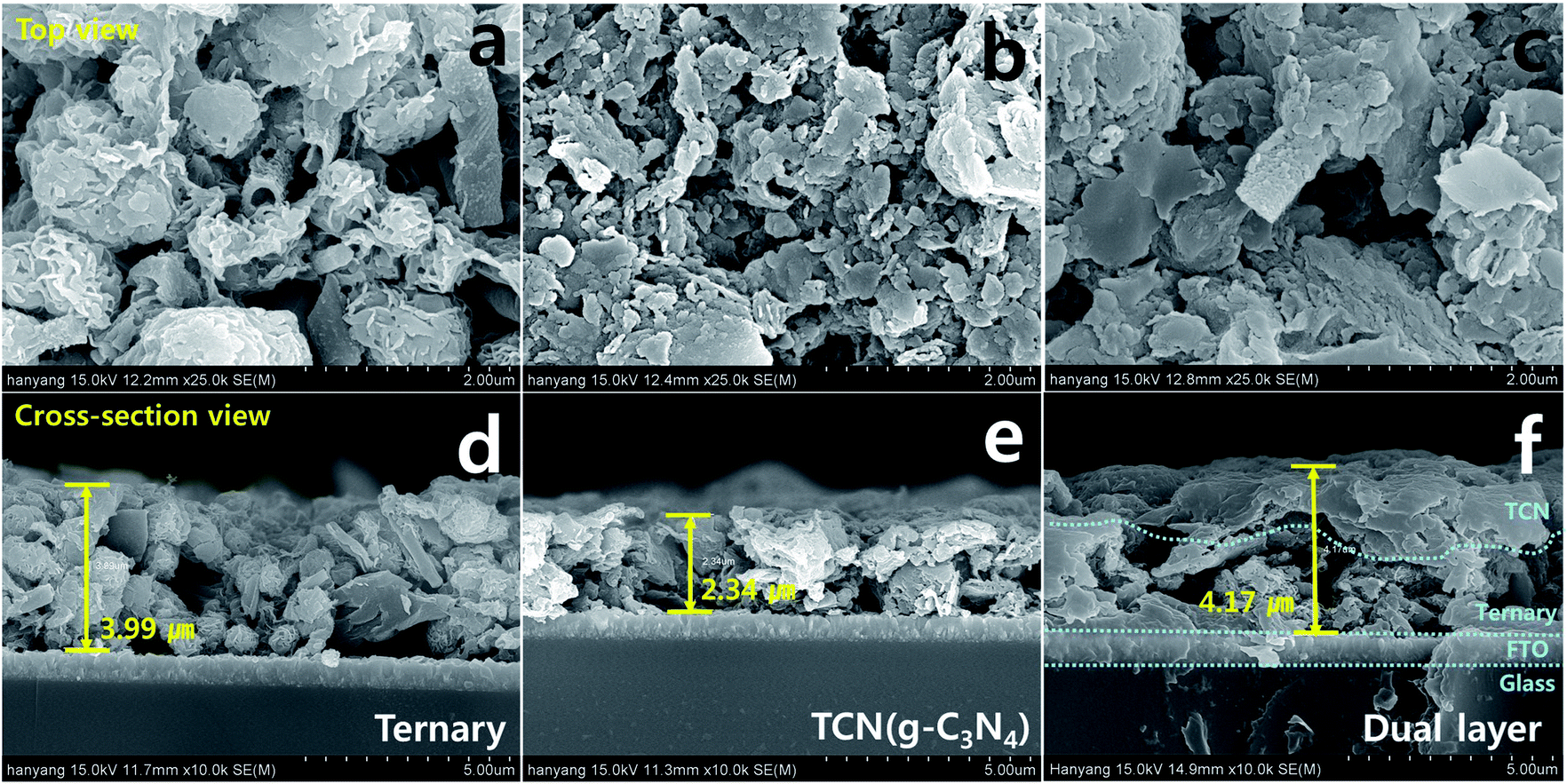 | ||
| Fig. 1 Top view scanning electron microscopy (SEM) images of (a) ternary film, (b) TCN film, and (c) dual layered film, and cross-sectional images of (d) ternary film, (e) TCN film, (f) and dual layered film (blue dotted lines indicate interfaces between different layers). | ||
The crystalline phases of the as-prepared samples were observed using XRD analysis, as shown in Fig. 2(a). The peaks for the crystalline MoS2 patterns appeared at 12.02, 33.34, 38.83 and 58.9°, which are indexed to the (002), (100), (103) and (110) planes (JCPDS no. 37-1492),28 respectively. In the case of the ternary films, the sharp diffraction peaks indicate high crystallinity of MoS2. We observed the g-C3N4 peak from the TCN and dual layered films at 27.3°, which corresponds to the (002) plane, indicating the inter-planar spacing of aromatic systems.29 Due to the photoanode film of the FTO substrate, the diffraction peaks of the SnO2 phase were detected by XRD analysis according to JCPDS no. 01-070-6995.30 We also used FT-IR to analyze the chemical molecular composition of the g-C3N4 structures. The ternary, bare TCN and dual layered films exhibited C–N heterocycles at wavenumbers 1577.8, 1399.6, 1313.2, 1131.8 cm−1, and s-triazine units at 806.8 cm−1. For the ternary film, it showed graphene-related FT-IR peaks of C–O–C, C–O and C–OH at 1212.2, 1146.7 and 1057.1 cm−1, respectively since the ternary structure is surrounded by sulfur/nitrogen-doped graphene (SNG).31,32 As shown in Fig. 2(b), the g-C3N4 specific groups were shifted when the TCN was coated on ternary structures. The heterocycle rings of dual layered film were detected at 1577.9, 1400.5, 1312.9, 1124.3 cm−1, which we attributed to the aromatic C![[double bond, length as m-dash]](https://www.rsc.org/images/entities/char_e001.gif) N and C–N stretching vibration. Furthermore, s-triazine units for graphite-like sp2 bonding state were presented at 804.9 cm−1 due to the breathing mode.33 The broad peaks at 3400–3000 cm−1 denoted amine (N–H) and hydroxyl (O–H) stretching modes.34 Based on the results of our XRD and FT-IR analysis, the dual layered film was well formed, coating ternary structures with TCN.
N and C–N stretching vibration. Furthermore, s-triazine units for graphite-like sp2 bonding state were presented at 804.9 cm−1 due to the breathing mode.33 The broad peaks at 3400–3000 cm−1 denoted amine (N–H) and hydroxyl (O–H) stretching modes.34 Based on the results of our XRD and FT-IR analysis, the dual layered film was well formed, coating ternary structures with TCN.
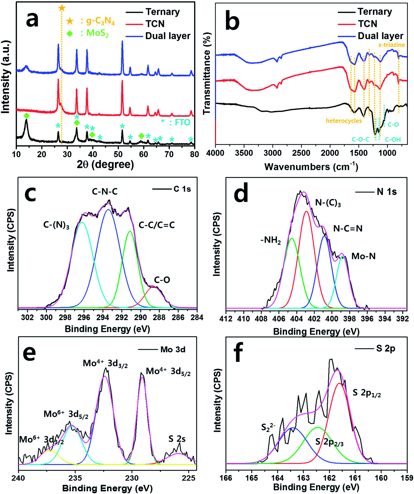 | ||
| Fig. 2 Characterization analysis of ternary film, TCN film and dual layered film. (a) X-ray diffraction, and (b) Fourier transform infrared and X-ray photoelectron spectroscopy fitting data on dual layered film of (c) C 1s, (d) N 1s, (e) Mo 3d and (f) S 2p. | ||
To confirm the characterization of the g-C3N4 and ternary structures of the dual layered film, we carried out XPS fitting analysis to investigate the chemical bonding based on the binding energy. In the C 1s spectrum (Fig. 2(c)), the main three Gaussian peaks were deconvoluted at 291.1, 293.4 and 296.2 eV, which we assigned to the graphitic carbon bonding of the C–C/CC, N atoms in the lattice of the g-C3N4 group with defect sp3 carbon atoms in C–N–C, and to sp2-hybridized carbon in the triazine group of C–(N)3, respectively.35 The peak of the C–O bond at 288.6 eV was attributed to the O2 species around the sp2-hybridized carbon in the g-C3N4.36 The main peaks in the N 1s spectrum were assigned to sp2-hybridized N2 of C–NC (400.9 eV), and tertiary N2 of N–(C)3 (404.6 eV) and –NH2 (402.9 eV), as shown in Fig. 2(d).37 In particular, we made novel observations of Mo–N bonding at 398.8 eV, which indicated the deep heterojunction between g-C3N4 and MoS2.29 The obtained main peaks for Mo4+ 3d5/2 and Mo4+ 3d3/2 were centered at 229.1 and 232.4 eV, respectively, providing typical values of Mo4+ species, as shown in Fig. 2(e). The peaks were observed at 235.3 eV for Mo6+ 3d5/2 and 237.3 eV for Mo6+ 3d3/2, possibly due to slight oxidation of the MoS2 surface into molybdenum oxide (MoO3).38,39 Theoretically, XRD identifies the crystalline phase of the materials within its thickness of 10 μm from the surface while XPS identifies the oxidation state of the materials from the chemical binding energies even with ultra-thin layer.40,41 Thus, slight oxidation of MoO3 from the surface of MoS2 was estimated based on the detection of Mo6+ peaks from XPS analysis although MoO3 was not detected in XRD analysis.42 The peak was located at 225.9 eV, which we attributed to S 2s. Fig. 2(f) indicates two strong peaks at 161.6 and 162.4 eV, corresponding to S 2p2/3 and S 2p1/3, respectively, in the S 2p spectrum of the dual layered film. Moreover, a broad peak was observed at 162.8 eV, indicating bridged S22− or apical S2−.43,44. Therefore, these observations confirmed the successful formation of dual layered film using ternary structures with TCN.
3.2 Optical properties for band diagram
We also assessed the optical properties of the samples to evaluate their absorbance properties with respect to their band gap energy. As shown in Fig. 3(a), the ternary film exhibited higher absorption than TCN or dual layered films in the UV-VIS region, without band edges. Due to the black color of the film, only the ternary film absorbed the entire light spectrum, while both the TCN and dual layered films exhibited a band edge in the visible region at a wavelength of approximately 450 nm, suggesting higher activity than bare ternary film when exposed to light. Moreover, the dual layered film exhibited increased absorption in the visible region compared to that of TCN film. We calculated the band gap energies of the TCN and dual layered films, as shown in Fig. 3(b). The band gap energy of the TCN film showed the typical bulk g-C3N4 band gap energy to be 2.56 eV.14 If the ternary structures and TCN were formed as a dual layer, the band gap would obviously be shifted into lower energy, corresponding to our measured value of 1.64 eV. The photoluminescence (PL) was measured to obtain the recombination of charge carrier status for the as-prepared films under excitation laser of 325 nm. As a result, there was no emission of PL intensity observed from the ternary structure as shown in Fig. S2.† The TCN film exhibited the highest PL intensity, while the dual layered film exhibited the lowest PL intensity. Based on our PL results (Fig. 3(c)), it can be seen that the dual layer formed successful heterostructures between the ternary composite and the TCN, promoting reduction of the recombination of photo-excited electron–hole pairs. We analyzed the transient photocurrent to observe the responses of the samples to visible irradiation. The photocurrent was measured by light-chopping in on–off cycles. In Fig. 3(d), the TCN and dual layered film exhibited photocurrents of 0.5 and 12.6 μA, respectively. When the light was on, both films exhibited a steady-state photocurrent.45 However, when the light was off, interestingly, the photo-response of the dual layered film was much slower than that of the TCN. The slow photocurrent indicated superior charge carrier separation, increasing the carrier lifetime. Thus, the dual layered film reduces the recombination rate through the interface between the ternary structures and TCN, yielding a 25-fold improvement in the photo-response under visible illumination.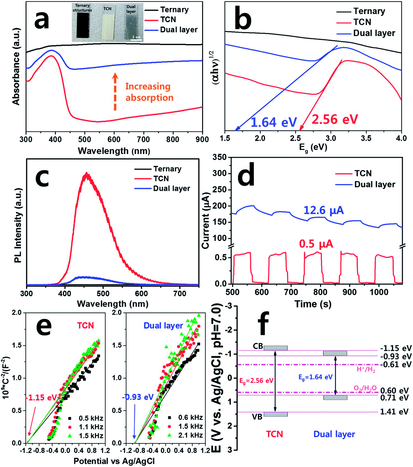 | ||
| Fig. 3 Photoresponse analysis of (a) optical absorbance (inset; image of films), (b) calculated band gap energy, (c) photoluminescence of ternary film, TCN film and dual layered film, and (d) transient photocurrent, (e) flat band potential analysis using Mott–Schottky measurement and (f) band diagram of TCN film and dual layered film. | ||
To determine the band structure of the as-prepared films, flat band potential was measured and plotted using Mott–Schottky. As shown in Fig. 3(e), the TCN and dual layered film indicated positive slopes in the plots, suggesting n-type semiconductors. The flat band potential of both TCN and dual layered film are shown to be independent of different frequencies from the same x-intercept. The flat band potentials of TCN and dual layer are estimated to be –1.15 and −0.93 eV, respectively. For the case of n-type semiconductors, the flat band potentials are equal to that of CB (conduction band) and the estimated flat potential value can be acted as the potential for CB. According to the bandgap measurement with flat band potential, the VBs (valence bands) of TCN and dual layer were calculated to be 1.41 and 0.71 eV, respectively. Finally, the band diagram of TCN and dual layered film was shown in Fig. 3(f), confirming that dual layer can facilitate the electron and hole pairs during the photocatalytic performances compared to that of TCN film due to its suitable band position.
3.3 Methylene blue photodegradation
The MB photodegradation of the as-fabricated photoanode films was carried out under visible light illumination. Fig. S3(a)† shows the experimental set-up for photocatalytic degradation with a xenon-arc lamp using >400 nm cut-off filter. Fig. 4(a) and (b) demonstrate the MB pollutant absorbance of TCN and dual layered films against wavelengths between 600–650 nm. The photocatalytic degradation activity began at 0 min and continued up to full degradation at 300 min. When the light was illuminated, the photoanode film started to remove the MB pollutant over time. Commonly, bulk graphitic carbon nitride has shown the adsorption properties or organic dyes even under the dark condition. Due to its porous structure of graphitic carbon nitride, the dye can be adsorbed easily on that of surface.46 To verify the adsorption ability of as-prepared films, the photocatalytic performance was carried out under dark condition for 30 min. After that, the adsorption ability was clearly observed through optical absorbance analysis. As a result, TCN film has adsorbed 2.7% of the MB dye while the dual layered film showed much higher adsorption properties of 6.9% than that of TCN film due to dual layer of porous structure. Therefore, the TCN film has shown slight pollutant removal until 300 min. When the TCN was coated onto the ternary film, resulting in a dual layer of heterostructured film, the MB degradation proceeded faster than when pure TCN film was used, removing the organic pollutant after up to 300 min. We assessed the kinetic rate constant by calculating the MB concentration, which is plotted in Fig. 4(c). For comparison, pure MB degradation was monitored without a photoanode film under the same conditions and the blank solution shows the degradation results. Hence, MB degradation on photoanode films follows a pseudo-first-order equation, called the Langmuir–Hinshelwood (L–H) mechanism.47 The L–H mechanism is defined as:| −ln(C/C0) = kt | (1) |
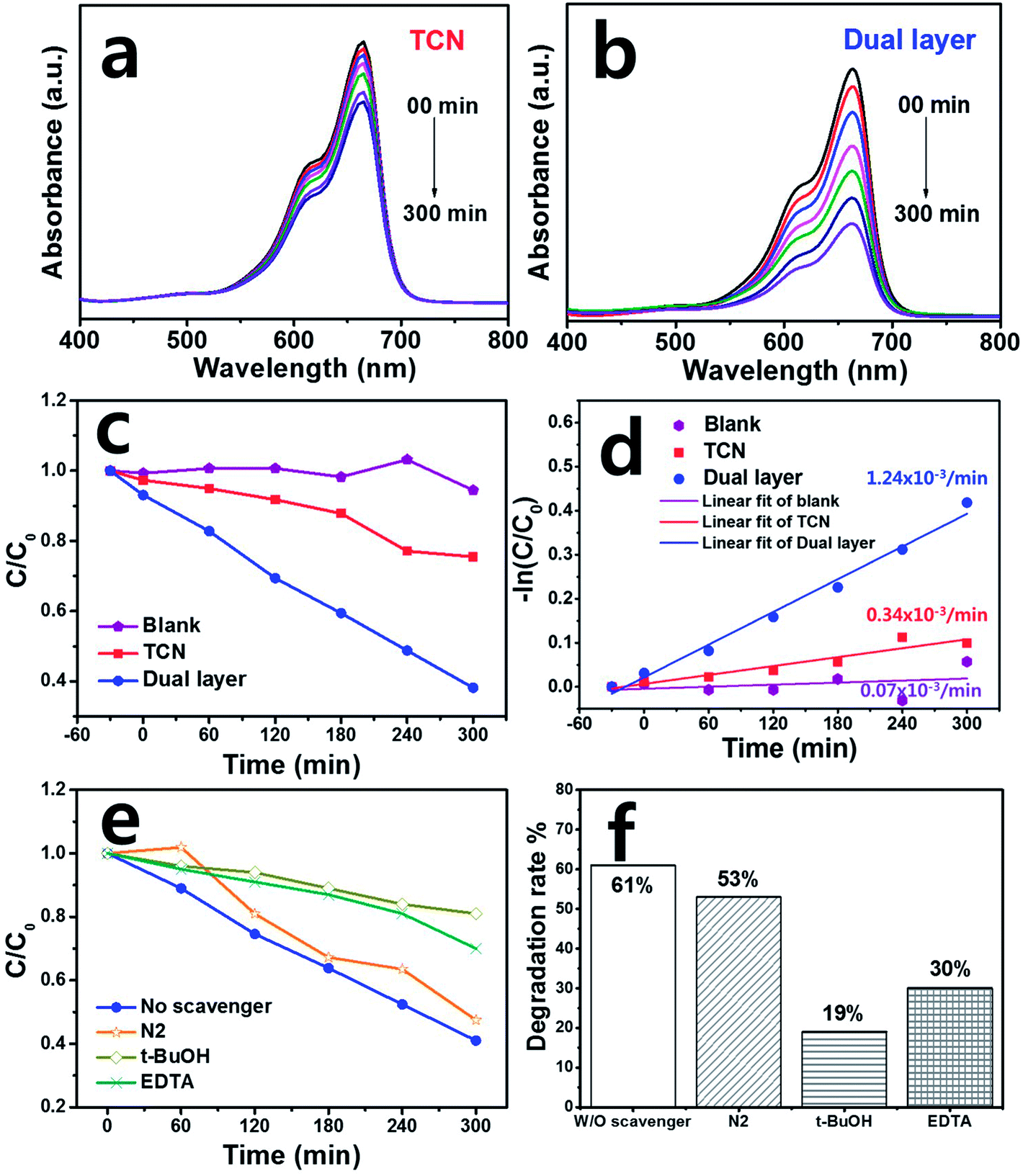 | ||
| Fig. 4 Photodegradation activity of methylene blue (MB) (a) TCN film, (b) dual layered film, (c) relative absorbance of MB degradation, (d) logarithmic absorbance of MB with kinetic rate constant on pure MB solution, TCN, dual layer and (e) scavenger test, (f) degradation efficiency based on scavenger test of w/o scavenger, N2, t-BuOH and EDTA under visible irradiation. | ||
Based on eqn (1), −ln(C/C0) showed linear plots and k is the kinetic rate constant (min−1) of the catalytic degradation activity.48 The k value of the dual layered film was calculated to be 1.24 × 10⁻³ min−1, which was about four times higher than that of TCN film (0.34 × 10⁻³ min−1), as shown in Fig. 4(d). In the case of the MB itself, the k value was calculated to be 0.07 × 10⁻³ min−1.
To study the photocatalytic mechanism in detail, the scavenger test of dual layer was carried out using EDTA·2Na (EDTA), t-butanol (t-BuOH) and nitrogen (N2) as hole (h+) capture, hydroxyl radical (·OH) and superoxide radical (·O2−), respectively under the same condition of the photocatalytic performance as shown in Fig. 4(e) and (f). The N2 was added into MB solution with dual layer, showing the similar degradation efficiency of 53% compared to that of dual layered film (61%). This demonstrated that superoxide radical was negligible in the photocatalytic reaction. However, when the t-BuOH and EDTA were added into methylene blue solution, the degradation rate of t-BuOH and EDTA decreased to lower the degradation efficiencies to be 19% and 30%, respectively compared to those of other scavengers. As a result, we can clearly see that h+ and ·OH were the main active species during the MB photocatalytic degradation activity.
The detailed photodegradation process is explained as follows: When visible light was irradiated onto the dual layered film, photoinduced electron and hole pairs were generated on the surface of the dual layered film. In the TCN conduction band, the electron (e−) transferred from the valence band reacted with the attached O2 molecules on the TCN surface to produce O2 radicals, ·O2−. The ·O2− radicals eventually degraded the MB dye into the water.49 Meanwhile, the hole (h+) from the TCN valence band reacted with the OH in the aqueous solution, producing ·OH radicals. This then reacted with the MB dye molecules via the oxidation reaction, degrading the products into water.50 According to the photodegradation results, the dual layered film exhibited remarkable photocatalytic removal under MB pollutant, leading to effective separation of the photo-excited electron and hole pairs between the ternary structures and TCN interface, further promoting photo-redox reactions and the excellent removal of MB organic pollutant on the surface of the TCN film.
3.4 H2 evolution and EIS measurements
We investigated the hydrogen (H2) evolution in more detail to evaluate the photoanode film itself under visible light irradiation. Fig. S3(b)† is the set-up for H2 evolution of the as-prepared films with a xenon-arc lamp using a > 400 nm cut-off filter. As shown in Fig. 5(a), the TCN and dual layered films exhibited H2 production over 5 hours. The dual layered film exhibited lower activity than the TCN film when the gas was collected during the first hour. However, significantly higher H2 activity occurred in the dual layered film than in the TCN film after 2 hours. Up to 5 hours, the dual layered film exhibited H2 production of 44.9 μmol, which is almost four times higher than that of the TCN film, of 11.1 μmol. After 5 hours of reaction time in the case of TCN film, the H2 evolution decreased slightly compared to the activity at 4 hours, suggesting both poor stability and photo-response. To assess the stability of the dual layered film, a recycling test was carried out for 10 cycles and the results are shown in Fig. 5(b). For the same experimental state, N2 gas was bubbled into the aqueous solution and then Ar was purged into the reactor after every cycle was completed. During the repeatability test, we observed almost stable H2 activities over 45 hours, except for a few cycles in which H2 production decreased. Therefore, the dual layered film exhibited superior H2 production compared to the TCN film over time. This was due to the proper interaction between the ternary structure and the TCN, enabling successful separation of charge carriers under light irradiation.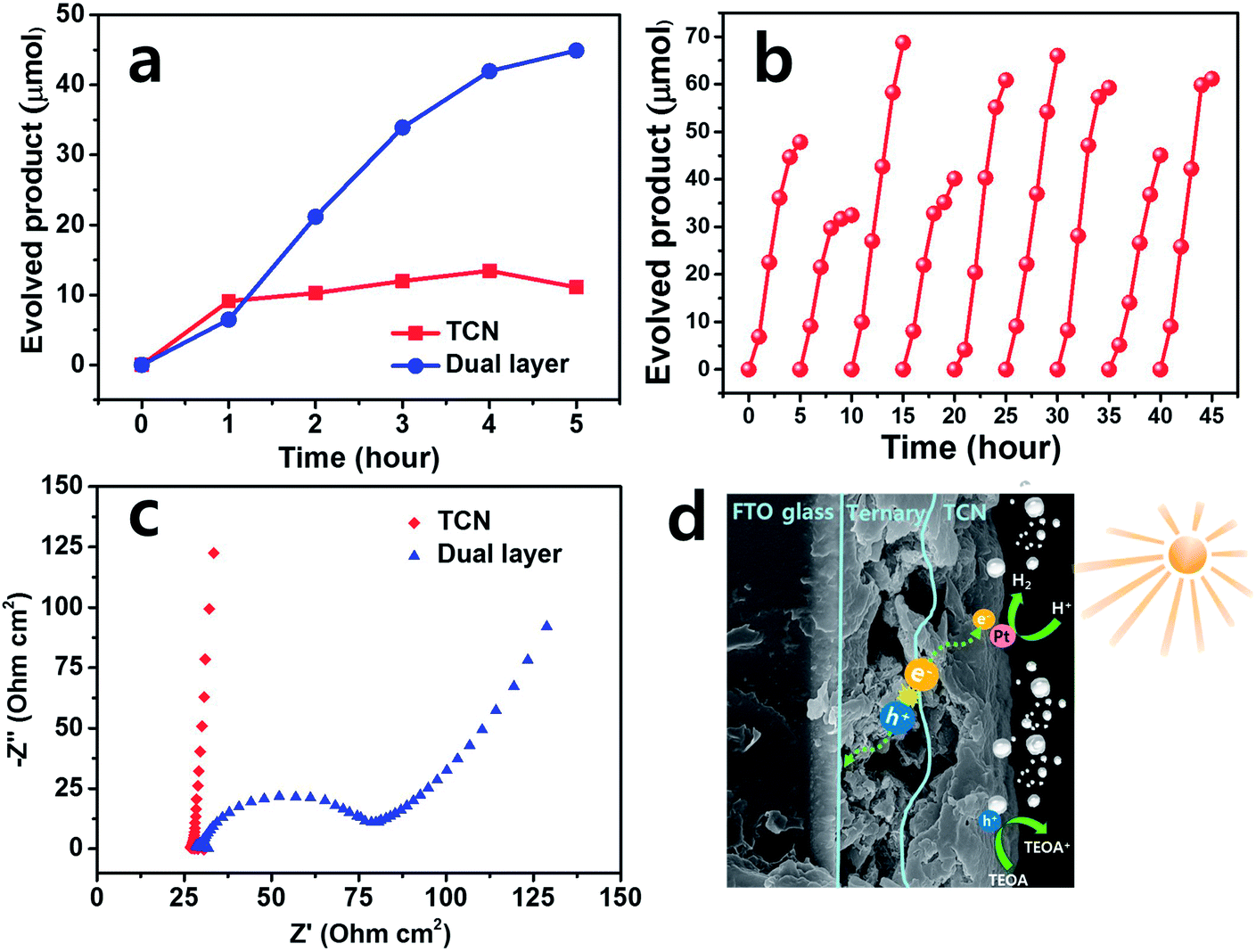 | ||
| Fig. 5 (a) Hydrogen (H2) evolution on TCN film and dual layered film, (b) H2 evolution recycle tests on dual layered film, (c) electrochemical impedance spectroscopy (EIS) measurement on TCN film and dual layered film and (d) its possible mechanism. | ||
Based on these H2 production results, we used EIS measurements to measure the resistance of the photoanode film, to elucidate the relationship between the electrolyte and the heterostructures of the as-prepared film. The Nyquist plot usually exhibits charge transfer resistance with an arc radius, as shown in Fig. 5(c). The smaller semicircle of the dual layered film was observed to be ∼50 ohm cm2, while the larger plot of the TCN film was observed to be ∼2500 ohm cm2 under visible light irradiation, as shown in Fig. S2.† Thus, these EIS results confirm that the dual layered film successfully formed heterojunctions with ternary structures/TCN, as expected, reducing the interface resistance between these heterostructures and electrolyte.
Consequently, a possible mechanism can be inferred from the H2 evolution, EIS measurements as shown in Fig. 5(d). When the dual layered film was illuminated by visible light, the electron–hole pairs were generated on the surface of the ternary film. Initially, the electrons (e−) were photogenerated from TCN film. Afterwards, these electrons were shifted to the Pt on the surface of the TCN film, producing H2 gas. Meanwhile, the photo-induced holes (h+) from TCN film were transferred to the ternary structures and then FTO substrate. The remaining holes in the valence band of the TCN film were captured by the TEOA, promoting H2 evolution.51,52 The interface between ternary structures and TCN acted as channels to connect as heterojunctions as well as transportation of electron and hole pairs, which both prohibits the recombination of photo-induced charge carriers and promotes excellent photocatalytic activities. Therefore, the dual layered film effectively separated the electron–hole pairs at the heterojunction interface, developing stable H2 evolution activity compared to bare TCN film.
4. Conclusion
We designed two different composites of ternary structures, HGCNF/MoS2/SNG and bulk g-C3N4 from a thiourea precursor (TCN) prepared as a dual layered film using a spin coating method, for photo-responsible applications. The formation of TCN-based dual layered films on the ternary structures was well-characterized, and we identified the morphological structures and individual chemical bonds. These simplified dual layered structures revealed increasing absorption in the visible region, with a decreased band gap energy compared to bare TCN film. Moreover, the dual layered film reduced recombination rates and produced a high photoresponse due to the effective charge carrier separation, as demonstrated by our PL and transient photocurrent analysis. Based on the characterization of the as-prepared films, the dual layered film exhibited exceptional photodegradation kinetic activity of 1.24 × 10⁻³ min−1 and H2 evolution of 44.9 μmol over 5 hours, with steady stability under visible light irradiation for 45 hours. Furthermore, a low impedance value of ∼50 ohm cm2 was observed in the dual layered film, suggesting that the interface between ternary structures and bulk g-C3N4 reduced its resistance based on the EIS measurement. Therefore, compared to bare TCN film under visible light, our photodegradation and H2 evolution results indicate that the dual layered film composed of ternary structures and TCN improved the photo-response capabilities by facilitating the effective separation of the photo-induced electron–hole pairs.Conflicts of interest
There is no conflict to declare.Acknowledgements
This work was supported by a National Research Foundation of Korea (NRF) grant funded by the Korean government (Ministry of Education) (No. NRF-2016R1D1A1A02936936) and a NRF grant funded by the Korean government (MEST) (No. NRF-2018R1A2A1A13078704), and the Human Resources Development program (No. 20174030201830) of a Korea Institute of Energy Technology Evaluation and Planning (KETEP) grant funded by the Korea government Ministry of Trade, Industry and Energy.References
- M. R. Hoffmann, S. T. Martin, W. Choi and D. W. Bahnemann, Chem. Rev., 1995, 95, 69–96 CrossRef CAS.
- O. Legrini, E. Oliveros and A. M. Braun, Chem. Rev., 1993, 93, 671–698 CrossRef CAS.
- M. G. Lee, J. S. Park and H. W. Jang, J. Korean Ceram. Soc., 2018, 55, 185–202 CrossRef CAS.
- A. Fujishima and K. Honda, Nature, 1972, 238, 37 CrossRef CAS.
- A. Fujishima, T. N. Rao and D. A. Tryk, J. Photochem. Photobiol. C Photochem. Rev., 2000, 1, 1–21 CrossRef CAS.
- A. L. Linsebigler, G. Lu and J. T. Yates, Chem. Rev., 1995, 95, 735–758 CrossRef CAS.
- W. Cui, J. He, H. Wang, J. Hu, L. Liu and Y. Liang, Appl. Catal. B Environ., 2018, 232, 232–245 CrossRef CAS.
- Y. Zhang, W. Cui, W. An, L. Liu, Y. Liang and Y. Zhu, Appl. Catal. B Environ., 2018, 221, 36–46 CrossRef CAS.
- H. Wang, Y. Liang, L. Liu, J. Hu and W. Cui, J. Hazard. Mater., 2018, 344, 369–380 CrossRef CAS PubMed.
- Q. Xiang, J. Yu and M. Jaroniec, J. Am. Chem. Soc., 2012, 134, 6575–6578 CrossRef CAS PubMed.
- J. B. Priebe, J. Radnik, A. J. J. Lennox, M.-M. Pohl, M. Karnahl, D. Hollmann, K. Grabow, U. Bentrup, H. Junge, M. Beller and A. Brückner, ACS Catal., 2015, 5, 2137–2148 CrossRef CAS.
- H.-L. Liu and T. C. K. Yang, Process Biochem., 2003, 39, 475–481 CrossRef CAS.
- C. Wang, B.-Q. Xu, X. Wang and J. Zhao, J. Solid State Chem., 2005, 178, 3500–3506 CrossRef CAS.
- J. Wen, J. Xie, X. Chen and X. Li, Appl. Surf. Sci., 2017, 391, 72–123 CrossRef CAS.
- L. Yang, W. Zhou, D. Hou, K. Zhou, G. Li, Z. Tang, L. Li and S. Chen, Nanoscale, 2015, 7, 5203–5208 RSC.
- C. Zhang, Z. Wang, S. Bhoyate, T. Morey, L. B. Neria, V. Vasiraju, G. Gupta, S. Palchoudhury, K. P. Kahol, R. S. Mishra, F. Perez and K. R. Gupta, C, 2017, 3, 33 Search PubMed.
- C. Mu, Y. Zhang, W. Cui, Y. Liang and Y. Zhu, Appl. Catal. B Environ., 2017, 212, 41–49 CrossRef CAS.
- X. Wang, Y. Liang, W. An, J. Hu, Y. Zhu and W. Cui, Appl. Catal. B Environ., 2017, 219, 53–62 CrossRef CAS.
- H. Wang, Y. Liang, L. Liu, J. Hu, P. Wu and W. Cui, Appl. Catal. B Environ., 2017, 208, 22–34 CrossRef CAS.
- A. K. Geim and K. S. Novoselov, Nat. Mater., 2007, 6, 183 CrossRef CAS PubMed.
- M. E. M. Buan, N. Muthuswamy, J. C. Walmsley, D. Chen and M. Rønning, ChemCatChem, 2017, 9, 1663–1674 CrossRef CAS.
- T. F. Jaramillo, K. P. Jørgensen, J. Bonde, J. H. Nielsen, S. Horch and I. Chorkendorff, Science, 2007, 317, 100 CrossRef CAS.
- M. Kotal, J. Kim, K. J. Kim and I.-K. Oh, Adv. Mater., 2016, 28, 1610–1615 CrossRef CAS.
- F. He, G. Chen, Y. Yu, S. Hao, Y. Zhou and Y. Zheng, ACS Appl. Mater. Interfaces, 2014, 6, 7171–7179 CrossRef CAS PubMed.
- Y. Sun and K. Yan, J. Adv. Oxid. Technol., 2016, 19, 376 CAS.
- N. Nalajala, K. K. Patra, P. A. Bharad and C. S. Gopinath, RSC Adv., 2019, 9, 6094–6100 RSC.
- S. Kang, J. Jang, S.-h. Ahn and C. S. Lee, Dalton Trans., 2019, 48, 2170–2178 RSC.
- L. Yang, X. Cui, J. Zhang, K. Wang, M. Shen, S. Zeng, S. A. Dayeh, L. Feng and B. Xiang, Sci. Rep., 2014, 4, 5649 CrossRef CAS PubMed.
- W. Fu, H. He, Z. Zhang, C. Wu, X. Wang, H. Wang, Q. Zeng, L. Sun, X. Wang, J. Zhou, Q. Fu, P. Yu, Z. Shen, C. Jin, B. I. Yakobson and Z. Liu, Nano Energy, 2016, 27, 44–50 CrossRef CAS.
- A. Enesca, L. Isac and A. Duta, Appl. Catal. B Environ., 2015, 162, 352–363 CrossRef CAS.
- Y. Byun, M. Cho, D. Kim, Y. Jung and A. Coskun, Macromolecules, 2017, 50, 523–533 CrossRef CAS.
- J. Yuan, G. Chen, W. Weng and Y. Xu, J. Mater. Chem., 2012, 22, 7929–7936 RSC.
- B. Zhu, P. Xia, W. Ho and J. Yu, Appl. Surf. Sci., 2015, 344, 188–195 CrossRef CAS.
- F. Dong, Y. Li, Z. Wang and W.-K. Ho, Appl. Surf. Sci., 2015, 358, 393–403 CrossRef CAS.
- L. Ma, H. Fan, K. Fu, S. Lei, Q. Hu, H. Huang and G. He, ACS Sustainable Chem. Eng., 2017, 5, 7093–7103 CrossRef CAS.
- J. Li, B. Shen, Z. Hong, B. Lin, B. Gao and Y. Chen, Chem. Commun., 2012, 48, 12017–12019 RSC.
- P.-K. Chuang, K.-H. Wu, T.-F. Yeh and H. Teng, ACS Sustainable Chem. Eng., 2016, 4, 5989–5997 CrossRef CAS.
- L. Ye, D. Wang and S. Chen, ACS Appl. Mater. Interfaces, 2016, 8, 5280–5289 CrossRef CAS.
- M.-h. Wu, L. Li, Y.-c. Xue, G. Xu, L. Tang, N. Liu and W.-y. Huang, Appl. Catal. B Environ., 2018, 228, 103–112 CrossRef CAS.
- S. J. Kerber, T. L. Barr, G. P. Mann, W. A. Brantley, E. Papazoglou and J. C. Mitchell, J. Mater. Eng. Perform., 1998, 7, 329–333 CrossRef CAS.
- M. N. Islam, T. B. Ghosh, K. L. Chopra and H. N. Acharya, Thin Solid Films, 1996, 280, 20–25 CrossRef CAS.
- H. Li, F. Xie, W. Li, B. D. Fahlman, M. Chen and W. Li, RSC Adv., 2016, 6, 105222–105230 RSC.
- J. E. Lee, J. Jung, T. Y. Ko, S. Kim, S.-I. Kim, J. Nah, S. Ryu, K. T. Nam and M. H. Lee, RSC Adv., 2017, 7, 5480–5487 RSC.
- X. Zheng, J. Xu, K. Yan, H. Wang, Z. Wang and S. Yang, Chem. Mater., 2014, 26, 2344–2353 CrossRef CAS.
- L. Hu, X. Liu, S. Dalgleish, M. M. Matsushita, H. Yoshikawa and K. Awaga, J. Mater. Chem. C, 2015, 3, 5122–5135 RSC.
- L.-R. Zou, G.-F. Huang, D.-F. Li, J.-H. Liu, A.-L. Pan and W.-Q. Huang, RSC Adv., 2016, 6, 86688–86694 RSC.
- H. Li, Y. Jing, X. Ma, T. Liu, L. Yang, B. Liu, S. Yin, Y. Wei and Y. Wang, RSC Adv., 2017, 7, 8688–8693 RSC.
- A. Ali and W.-C. Oh, J. Korean Ceram. Soc., 2017, 54, 205–210 CrossRef CAS.
- F. Wu, X. Li, W. Liu and S. Zhang, Appl. Surf. Sci., 2017, 405, 60–70 CrossRef CAS.
- T. J. Park, R. C. Pawar, S. Kang and C. S. Lee, RSC Adv., 2016, 6, 89944–89952 RSC.
- R. R. Prabhakar, W. Septina, S. Siol, T. Moehl, R. Wick-Joliat and S. D. Tilley, J. Mater. Chem. A, 2017, 5, 23139–23145 RSC.
- E. Pastor, F. Le Formal, M. T. Mayer, S. D. Tilley, L. Francàs, C. A. Mesa, M. Grätzel and J. R. Durrant, Nat. Commun., 2017, 8, 14280 CrossRef CAS.
Footnote |
| † Electronic supplementary information (ESI) available. See DOI: 10.1039/c9ra02074h |
| This journal is © The Royal Society of Chemistry 2019 |