
 Open Access Article
 This Open Access Article is licensed under a Creative Commons Attribution-Non Commercial 3.0 Unported Licence
Anomalous kinetic roughening in growth of MoS2 films under pulsed laser deposition†
Gobinda Pradhan‡
,
Partha P. Dey‡ and
Ashwini K. Sharma*
and
Ashwini K. Sharma*
Department of Physics, Indian Institute of Technology Guwahati, Guwahati – 781039, Assam, India. E-mail: aksharma@iitg.ac.in; Fax: +91-361-258-2749; Tel: +91-361-258-2724
First published on 26th April 2019
Abstract
Growth dynamics of thin films expressed by scaling theory is a useful tool to quantify the statistical properties of the surface morphology of the thin films. To date, the growth mechanism for 2D van der Waals materials has been rarely investigated. In this work, an experimental investigation was carried out to identify the scaling behavior as well as the growth mechanism of 2D MoS2 thin films, grown on glass substrates by pulsed laser deposition for different deposition time durations, using atomic force microscopy images. The growth of MoS2 films evolved from layer-by-layer to layer plus island with the increase in deposition time from 20 s to 15 min. The film surface exhibited anisotropic growth dynamics in the vertical and lateral directions where RMS roughness varied with deposition time as w ∼ tβ with the growth exponent β = 0.85 ± 0.11, while the lateral correlation length ξ was ξ = t1/z with 1/z = 0.49 ± 0.09. The films showed a local roughness exponent αloc = 0.89 ± 0.01, global roughness exponent α = 1.72 ± 0.14 and spectral roughness exponent αs = 0.85 ± 0.03, suggesting that the growth of MoS2 thin films followed intrinsic anomalous scaling behavior (αs < 1, αloc = αs ≠ α). Shadowing owing to conical incoming particle flux distribution towards the substrate during deposition has been attributed to the anomalous growth mode. The optical properties of the films, extracted from ellipsometric analysis, were also correlated with RMS roughness and cluster size variation which unveiled the important role played by surface roughness and film density.
1. Introduction
Transition metal dichalcogenides (TMDCs) are an emerging class of two-dimensional (2D) material with interesting electronic and optical properties.1–3 Among all the TMDC materials, MoS2 has drawn remarkable attention with its excellent semiconductor behavior like a tunable band gap of 1.2 (indirect)–1.9 (direct) eV, high electron mobility, high electronic on-off switching ratio, photoresponse etc.4–6 These properties make it more suitable than graphene for logic device applications. The true 2D nature makes MoS2 outperform Si transistors in terms of the nanoscale device limit.7,8 Recently, many MoS2-based devices have been demonstrated, including field effect transistors, integrated circuits and photo transistors.9–13 MoS2 nano-sheets also have an established efficacy as a catalyst for hydrogen evolution reaction and an electrode in super-capacitors.14–16 In the last few years, mono- and multilayered as well as bulk-like MoS2 films deposited via pulsed laser deposition (PLD) and their advanced applications in modern electronics and the optoelectronics field have been reported.17,18 The morphology and nanostructure of thin films strongly depend on the deposition method and growth conditions (i.e. duration, rate, temperature etc.).19,20 The surface morphology of thin films can control many of the physical and chemical properties (such as optical, catalytic, mechanical, electronic, etc.) which can strongly affect the device performance of the respective films. Therefore, understanding the growth dynamics of the deposited thin films is very important.The growth dynamics of thin films expressed by scaling theory is a useful tool to quantify the statistical properties of the surface morphology of thin films and to formulate theoretical models of growth modes for different inorganic materials such as metals, semiconductors, perovskite material etc.21–25 Scaling is often described in terms of a scaling function, describing certain aspects of a rough surface, which generally evolves with time but remain invariant with time only under certain scale transformations. In the past few decades, several theoretical models were proposed to relate the thin film growth mechanism to a set of scaling exponents.24,26–28 To the best of our knowledge, the growth mechanism of 2D van der Waals materials remains poorly investigated till date. The growth dynamics of MoS2 films using scaling functions under PLD were never reported which motivated us to undertake the following study.
We report on the evolution of surface morphology of a bi-layer to bulk-like MoS2 films to understand the growth dynamics and scaling behavior involved in MoS2 thin film growth under PLD. We have fitted the height–height correlation function (HHCF) with appropriate theoretical model to extract the interface width (w), lateral correlation length (ξ) as they evolve with deposition time. The film properties were quantified statistically in terms of short range (local) as well as long-range (global) roughness exponents (αloc and α), growth exponent (β), dynamic scaling exponent (z), etc. to determine the type of scaling and growth mechanism involved. This understanding can enable one to attain controlled growth of a film required in different applications. Spectroscopic ellipsometry (SE) studies enabled us to estimate the refractive index (n) and extinction coefficient (k) spectra for various film thicknesses. Their variation with increasing film thickness is correlated with RMS roughness (interface width w) and island size (correlation length ξ) variation which unveiled the important role played by surface roughness and film density. Such correlations have been rarely reported for 2D material. Moreover, the SE studies are also used to support the anomalous scaling behavior of film growth as concluded from AFM analysis.
2. Experiment
MoS2 thin films were deposited onto Corning glass substrate via PLD by focusing a 3rd harmonic of a Q-switched Nd:YAG laser (Spectra-Physics, pulse duration – 8 ns and repetition rate – 10 Hz) on polycrystalline MoS2 target (pellet), at a laser fluence ∼ 2.2 J cm−2 under vacuum (∼5 × 10⁻⁶ mbar). The films were deposited for various deposition times of 20 s, 1, 2, 5, 10 and 15 min duration at a substrate temperature of 600 °C. Raman spectra of the films were recorded (Horiba Jobin Yvon, LabRam HR 800) in the backscattering geometry using an excitation wavelength of 488 nm. X-ray diffraction measurements were carried out with the Cu Kα line in an X-ray diffractometer (Rigaku TTRAX III) at a glancing incidence angle of ω = 1°. The scanning range was 10° to 70° with an angular step of 0.03°. The surface morphology of all the films was recorded via AFM (Bruker-Innova) to study the dynamic scaling and growth mechanism of MoS2 films deposited via PLD technique. The SE measurements were carried out over the spectral range of 1.32–3.50 eV using Variable Angle Spectroscopic Ellipsometer (Semilab SOPRA: GES-5E) equipped with goniometer at incident angles of 65°, 70°, and 75°. Data acquisition and analysis were performed using spectroscopy ellipsometry analyzer (SEA) software. The analysis of SE data was carried out by screening several realistic physical models for semiconductors to obtain the best fit.29–32 In the present case, only the SE spectra recorded at incident angles of 70° is presented though the corresponding spectra at incident angles of 65°and 75° were also fitted with the same modeling which exhibited similar results.3. Results and discussions
3.1. Structural characterization of MoS2 films
Fig. 1 shows Raman spectra of MoS2 films for deposition time of 20 s, 1, 2, 5 min and MoS2 pellet in backscattering configuration. Each spectra exhibit twin peaks corresponding to A1g and E12g Raman modes of MoS2. The E12g and A1g Raman modes show layer sensitive peak positions. The peak position difference of A1g and E12g of MoS2 films increases with increase in layer numbers from monolayer to higher order.33 The Raman peak position difference of the deposited films are shown in the inset of Fig. 1.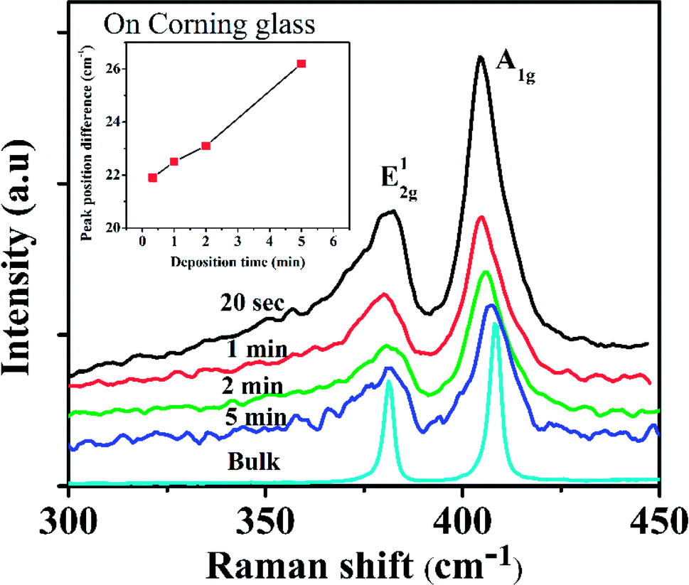 | ||
| Fig. 1 Raman spectra of the MoS2 films as a function of deposition time (t). | ||
The peak positions corresponding to A1g mode were observed at 404.9, 405.4, 405.6 and 406.2 cm−1 while that corresponding to E12g at around 383, 382.9, 382.5 and 380 cm−1 for the films deposited for time duration of 20 s, 1, 2 and 5 minutes, respectively. The peak difference between the two Raman modes, ΔF, in the respective films were found to be 21.9, 22.5, 23.1 and 26.2 cm−1, corresponding to bilayer, trilayer, multilayer and bulk-like MoS2 films.34,35 The Raman analysis of the films confirmed an increase in film thickness with the deposition time. Using surface profilometer the thicknesses of the films deposited for 1, 2, 5, 10 and 15 min deposition time are estimated to be 2.5, 6.4, 19.9, 39.6 and 81.2 nm, respectively while thickness of film deposited at 20 s could not be measured accurately due to much lower thickness (<2 nm). The XRD spectra of MoS2 films (ESI Fig. S1†) exhibits peaks at 2θ = 13.71° and 40.62° which corresponds to MoS2 (002) and MoS2 (103) planes, respectively, with former being more intense. The peak intensity of both peaks increased while the corresponding FWHM decreased with increasing deposition time as the MoS2 film thickness increased exhibiting increase in crystallinity.
3.2. Scaling studies of MoS2 film growth using AFM image analysis
The post growth surface morphology of the films was characterized systematically using AFM to study the surface microstructure and dynamics of the growth. Fig. 2(a)–(f) shows the AFM images of MoS2 films grown onto the Corning glass surfaces at 600 °C substrate temperature with 20 s, 1, 2, 5, 10 and 15 min deposition times, respectively.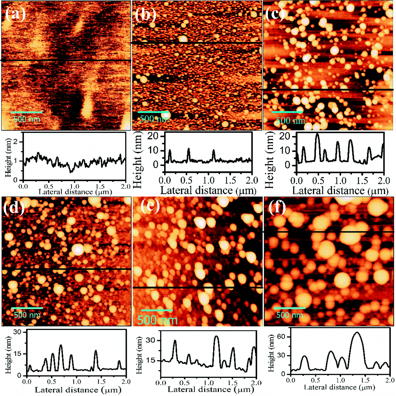 | ||
| Fig. 2 AFM images of top surface of PLD MoS2 films, showing the surface morphology for different deposition times (a) 20 s, (b) 1, (c) 2, (d) 5, (e) 10 and (f) 15 min. Each image consists of 2 × 2 μm scanned area and scale bar is 500 nm. Height profile of each image is shown at the bottom of the respective images. | ||
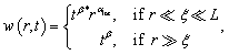
The AFM micrograph confirms that the grains are uniformly distributed within the film scanning area (2 μm × 2 μm). The scaling exponents (αloc, β, 1/z) have been estimated from the height–height correlation function (HHCF), H(r,t) by analyzing the surface morphology recorded using AFM to understand the growth processes and the dynamic scaling behavior involved during PLD of MoS2 films. H(r,t) is defined as statistical average of the mean square of height difference between two positions (x, y) and (x′, y′) on the surface separated by a distance 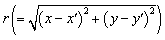 along horizontal direction as H(r,t) = 〈|h(r + r′,t) − h(r′,t)|2〉, where h(r + r′,t) and h(r′,t) are the heights of the surface at (x, y) and (x′, y′) and each pair of points are obtained from AFM image. HHCF can be evaluated from AFM images by spatial averaging over one or several regions, which should be much larger than r to avoid edge effects. HHCF shows two distinct behaviors based on the relative magnitudes of r and the lateral correlation length ξ; (i) for r ≪ ξ, H(r,t) ∼ [m(t)r]2α; where m(t) is the local slope and αloc (0 ≤ αloc ≤ 1) is the local roughness exponent, which describes short-range roughness of a self-affine surface, and (ii) for r ≫ ξ, H(r,t) ∼ 2w2, where
 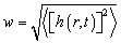 is the RMS roughness (interface width). w evolves following a simple dynamic scaling known as Family–Vicsek relation,
 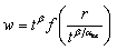 where
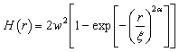
where 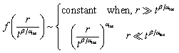 and r ≤ L (L is system size) while αloc and β are the roughness and growth exponents, respectively.36,37 The above relation suggests that for small r (i.e. r ≪ tβ/αloc), w is independent of deposition time t and scales as rαloc, but for large r, β is independent of r and follow the power laws as w ∼ tβ. The crossover between these two behaviors occurs at r = ξ, the lateral correlation length within which surface heights are significantly correlated. For dynamic scaling, the parameters w and ξ are dependent on the deposition time, t, and follow the power laws as w ∼ tβ and ξ ∼ t1/z.37 The set of exponents αloc, β and 1/z, corresponds to a specific universality class and is suggestive of the underlying mechanism that governs the evolution of surface. The HHCF can be defined by exponential correlation model, which satisfies the requirement for self-affine surface and manifests anisotropic scale invariance, given by,37
 | (1) |
From Fig. 3(a), it is observed that HHCF, H(r,t) increases linearly with r at small r and saturates at large r, with the asymptotic behavior predicted by eqn (1).37 It is clear from Fig. 3(a) that H(r,t) shifts upward as film thickness increases with increasing growth time, which confirms that the RMS roughness increases as the films grow, indicating roughening in the growth process.
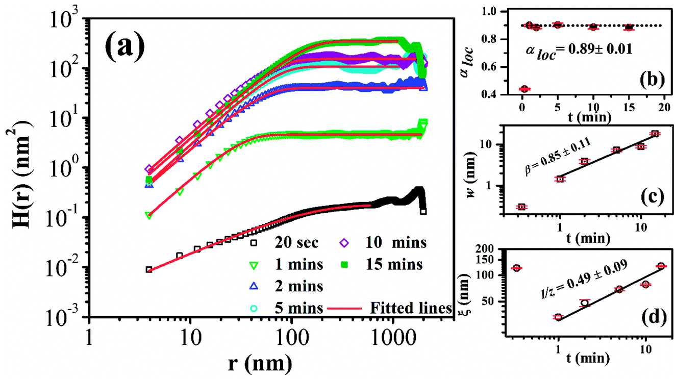 | ||
| Fig. 3 (a) log–log plot of HHCF, H(r) as a function of distance r with best fitted theoretical curve for MoS2 thin films on Corning glass substrate with different deposition times (20 s to 15 min). The symbols are experimental data and the red solid lines are fitted with eqn (1). Plot of (b) roughness exponent αloc, (c) surface roughness w, and (d) correlation length ξ as a function of deposition time, t. | ||
The HHCF curves were fitted using eqn (1), and w(t), ξ(t) as well as αloc were estimated. The variation of these parameters with deposition time were studied to understand the growth dynamics. Fig. 3(b) exhibits variation of αloc with time (t), while Fig. 3(c) and (d) shows log–log variations of w, and ξ versus t, respectively. From Fig. 3(b) it is observed that the value of αloc for the film deposited for 20 s was 0.41 and beyond that, it rises sharply and remains almost similar for all deposition time at around ∼0.89 ± 0.01. αloc lies between 0 to 1, where, a smaller value of αloc corresponds to the more locally rough surface while the larger αloc of the present films corresponds to locally smooth surface. Fig. 3(c) shows the increasing nature of w from 0.27 to 18.6 nm as the film grows with t from 20 s to 15 min and it clearly indicates the film roughening during growth. The parameters w showed power law dependency as w ∼ tβ with β = 0.85 ± 0.11. β is called growth exponent signifying the pace of surface roughening where β > 0.5 represents rapid roughening in thin films due to different non local effects like shadowing, high stickiness of substrate, bulk diffusion of incoming particles etc. Fig. 3(d) exhibits ξ versus t plot in logarithmic scale. Initially, at 20 s the value of ξ was 120.3 nm beyond which the value of ξ drops to 33.2 nm at 1 min deposition time. However, with increasing t from 1 to 15 min an increasing nature of ξ was observed, as shown in Fig. 3(d). This indicates that the lateral growth of the islands changes with time as ξ ∼ t1/z where 1/z = 0.49 ± 0.09. 1/z is called dynamics scaling exponent which corresponds to rate of lateral growth of correlated structure (islands). This confirms that as the deposition time increases, the islands grow both vertically as well as laterally and the overall film becomes rough. The lateral growth could be attributed to the increased nucleation of more incoming flux and the increase in crystallite size with increasing deposition time. The unusual large value of ξ at early stage of film growth at 20 s deposition time is due to layered (bilayer) MoS2 film growth supported by Raman results (Fig. 1). At this nucleation and growth stage only lateral growth takes place (following Frank–Van Der Merwe model) while with an increase in deposition time the vertical growth of the MoS2 film dominate over the lateral growth (following Sranski–Krastanov model) and the RMS roughness increases drastically as shown in Fig. 3(c).38
The TEM and FESEM images of films fabricated for 20 s (as shown in Fig. 4(a) and (b)) exhibit formation of bilayer without any cluster formation while that of 5 min film (Fig. 4(c) and (d)) show MoS2 clusters of various sizes sparsely distributed in uniform layered background film. The magnified TEM image (Fig. 4(e)) also shows the multilayer formation beneath the clusters. Hence, the transition of growth mode from layer-by-layer in the film fabricated at 20 s to layer plus island type for that deposited for longer duration observed in TEM and FESEM images is complementing the AFM results.
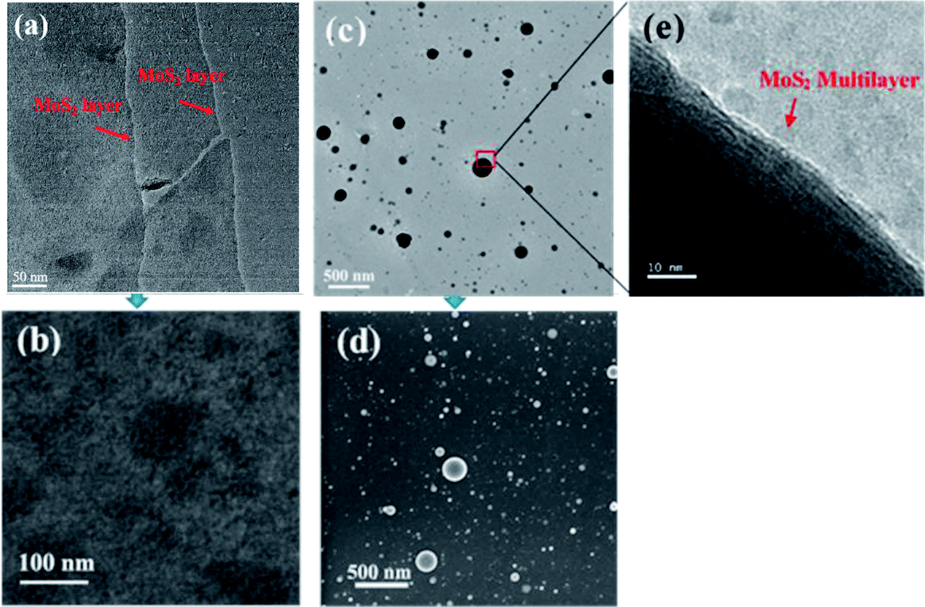 | ||
| Fig. 4 (a) TEM and (b) FESEM image of MoS2 film deposited for 20 s while (c) TEM and (d) FETEM image of MoS2 film deposited for 5 min and (e) high magnified TEM image of MoS2 cluster formed over the MoS2 film deposited for 5 min. | ||
For dynamic scaling to prevail, αloc = βz but in our case αloc ≠ βz, hence the dynamic scaling fails which implies that the scaling does not follow Family–Vicsek relation. In such a case, the height profile may follow another scaling hypothesis called anomalous scaling where the global and local interface widths scale differently and the global (α,β) and local (αloc,βloc) exponents are also different from each other. Such behavior has been observed where the conventional scaling laws can be modified by introducing new behavior in the interface width, w, which is represented by the anomalous scaling ansatz:
 | (2) |
 .37 If m(t) is independent of deposition time, it is called stationary type of growth. In stationary growth, for r < ξ the HHCF will merge for different t values. However, for the non-stationary case, H(r) will shift upward as the local slope, m(t), will change with the duration of deposition.21 In the present case, the growth is obviously non-stationary as m(t) was not constant. It was observed that the local slope, m(t) increases with time and varies as, m ∼ t0.41±0.11 as depicted in ESI Fig. S2.† Such a behavior where local slope m evolves with a power law in time, m(t) ∼ tβ* is observed for anomalous scaling.37,39 From this observation β* is found to be ∼0.41 ± 0.11 which is close to the value obtained from growth exponents.
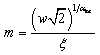
Now if we consider the combination of growth exponents α, β and z where α = βz, then under anomalous scaling also w ∼ tβ = tα/z. As ξ ∼ t1/z, one can easily observe that w ∼ ξα and the value of α can be found using the slope of log![[thin space (1/6-em)]](https://www.rsc.org/images/entities/char_2009.gif) w versus logξ as shown in Fig. 5. From the plot, the value α = 1.72 ± 0.14 was estimated, which is close with that obtained from α = βz ∼ 1.70 ± 0.13. The observed α > 1 suggest domination of vertical growth over the lateral growth i.e. the films roughening increases with the deposition time in the MoS2 films. The nonzero value of β* (as a result of inequality of α and αloc) indicates that scaling behaves anomalously and reconfirms the presence of a roughness exponent in global scale.
w versus logξ as shown in Fig. 5. From the plot, the value α = 1.72 ± 0.14 was estimated, which is close with that obtained from α = βz ∼ 1.70 ± 0.13. The observed α > 1 suggest domination of vertical growth over the lateral growth i.e. the films roughening increases with the deposition time in the MoS2 films. The nonzero value of β* (as a result of inequality of α and αloc) indicates that scaling behaves anomalously and reconfirms the presence of a roughness exponent in global scale.
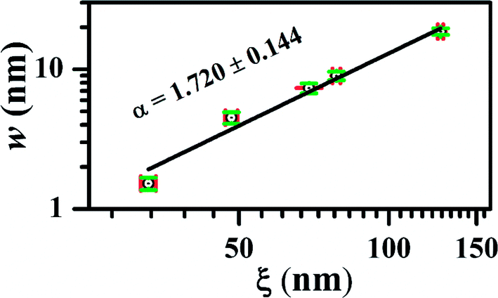 | ||
| Fig. 5 log–log plot of w versus ξ showing linear behavior. | ||
To further investigate the anomalous scaling behavior, the power spectral density function (PSDF) of the MoS2 films of various thicknesses were plotted in reciprocal space, k. The power spectral density function (PSDF) given as37  (ref. 37) is related to d-dimensional Fourier transform of surface heights, h(r,t) defined in reciprocal space, k. For an anomalous (d + 1) dimensional system, the PSD for anomalous scaling can be represented in frequency and time scale as,36,43,44
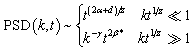 | (3) |
Fig. 6(a) shows log–log plot of PSD(k) versus k of the surfaces from the representative AFM images of MoS2 films deposited on glass substrates for the duration of 20 s, 1, 2, 5, 10 and 15 min. The PSD function does not show any characteristics peak at km inferring that the film grew as self-affine surface and not mounded.37 In the PSD spectra two distinct regions, k < t−1/z and k > t−1/z represented by eqn (3) are clearly visible. At lower k values PSD(k) is almost saturated for all the films while at higher k regimes PSD(k) value linearly decreases with k as PSD(k) ∼ k−(2αs+d) where d = 2 in our case. PSD value increases with deposition time and the transition point between linearly decreasing and saturated regions which corresponds to ∼1/ξ are shifted towards lower k regimes corresponds to an increase in island size (∼ξ) of the MoS2 films with time.
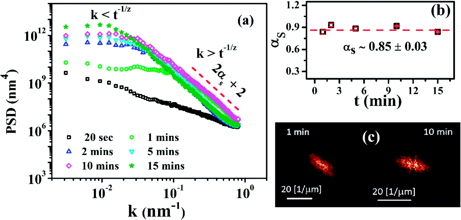 | ||
| Fig. 6 log–log plot of (a) PSD(k) as a function of k for MoS2 thin films deposited on the glass substrate with different deposition times. (b) Plot of αs of the MoS2 films as a function of deposition time. (c) 2D FFT pattern of the AFM images of MoS2 films deposited for 1 and 10 min. | ||
Fig. 6(b) shows the values of αs estimated from the slope of each PSD(k) plots (except that of the film deposited for 20 s) from k > t−1/z regime. The average value αs for the MoS2 films was observed to be ∼0.85 ± 0.03. The relevant exponents α, αs and αloc required for classifying the category of scaling are obtained from above analysis which shows that αloc (0.89 ± 0.01) ∼ αs (0.85 ± 0.03) ≠ α (1.72 ± 0.14) and αs < 1. This indicates an intrinsic anomalous scaling behavior for surface growth of the MoS2 thin films.36,43 Fig. 6(c) exhibits 2D fast Fourier transform (FFT) of AFM images corresponding to MoS2 films deposited for 1 min and 10 min. It shows a diffuse structure and absence of any bright ring like structure in k-space which support the self-affine like growth morphology excluding any type of mound formation in the surface of the films during growth.45
In order to further verify the anomalous scaling behavior of growth of the MoS2 films, we investigated the collapse of the HHCF and PSD dependent functions for different growth times. Under anomalous scaling, HHCF is given as,46
 | (4) |
 , behaves as,
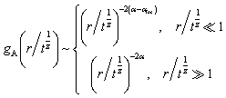
Hence the function H(r,t)/r2α when plotted as a function of  in log–log scale for different deposition times should collapse into single curve and from their slopes both α and αloc can be estimated.39 Similarly, PSD function can also be expressed under anomalous scaling as,39,46
 | (5) |
 , behaves as,
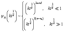
Hence the function PSD(k,t)k(2α+d) when plotted as a function of  in log–log scale for different deposition times should collapse into one curve and from their slopes both α and αs can be estimated. For our case, d = 2, hence
  .39 Fig. 7(a) and (b) exhibit the plot of logH(r,t)/r2α versus
  and plot of logPSD(k,t)k(2α+2) versus
  , respectively for the MoS2 films deposited for various time period (1–15 min). In Fig. 7(a), all the curves corresponding to different time period of growth collapsed to a single curve confirming the existence of anomalous scaling with slope values of 2 (α − αloc) ∼ 1.66 ± 0.01 and 2α ∼ 3.42 ± 0.02, for r/t1/z ≪ 1 and r/t1/z ≫ 1, respectively. From these slope the values of α and αloc are estimated to be 1.71 ± 0.01 and 0.88 ± 0.01, respectively, which are similar to their respective values obtained directly from HHFC analysis discussed above. Similarly, in Fig. 7(b), the collapse of all the PSD related curves, corresponding to different time period of growth, to a single curve confirming the existence of anomalous scaling with slope values of (2α + 2) ∼ 5.40 ± 0.17 for kt1/z ≪ 1 and 2 (α − αs) ∼ 1.69 ± 0.02 for kt1/z ≫ 1, respectively.39 The values of α and αs were extracted from the average values of slopes and are found to be 1.70 ± 0.08 and 0.85 ± 0.01, respectively. The values of α and αs obtained from the collapse of the PSD functions are also in agreement with the values obtained above. The inequality in α > 1 > αloc ∼ αs reconfirms the presence of intrinsic anomalous scaling in the present case.
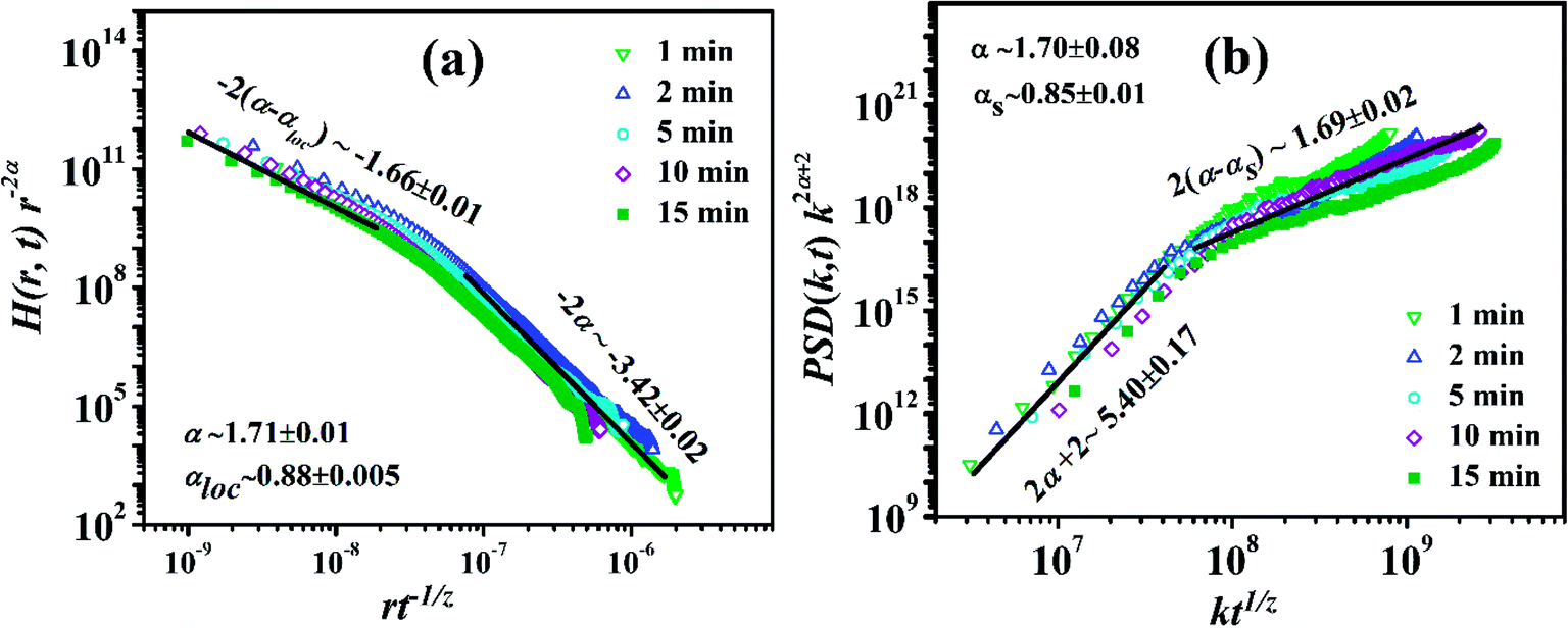 | ||
Fig. 7 Plots of (a) logH(r,t)/r2α versus  and (b) logPSD(k,t)k(2α+2) versus and (b) logPSD(k,t)k(2α+2) versus  showing data collapse of the anomalous scaling functions of the MoS2 films deposited for different time periods. showing data collapse of the anomalous scaling functions of the MoS2 films deposited for different time periods. | ||
Different local models like Mullins diffusion model,47 Edwards–Wilkinson model48 and KPZ model49 provide β = 0.25, 0 and 0.24, α = 1, 0 and 0.38 while z = 4, 2 and 1.58, respectively for 2 + 1 dimensions which does not match with the values of β, α and z observed in present case. Thus, none of the local models depicting different universality class can exactly explain the type of growth observed here. Although the exact mechanism has not been well understood, some studies in recent years have proposed that the anomalous kinetic roughening of the surfaces with a high growth exponent arises as consequences of nonlocal effects.50 Yao and Guo51 modified the non-local KBR model52 in sputtering growth where shadowing instability leads to the development of a mounded surface resulting w ∼ t1.0±0.04 and ξ ∼ t0.33±0.02. Moreover, Drotar et al.53 modeled the growth of a surface under shadowing (roughening effect) and higher zeroth-order sticking coefficient corresponds to minimal reemission (s0 = 1 and sn = 0 for n > 0), using a stochastic continuum growth equation,
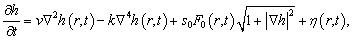 | (6) |
 , where θ is the local polar angle, Φ is the local azimuthal angle and R(θ,Φ) is the distribution of the incoming flux. They simulated the film surface growth using eqn (6) by Monte Carlo method in 2 + 1 dimensions giving β = 1 and 1/z = 0.93 ± 0.01. The β value predicted by the model formulated by Yao et al.51 and Drotar et al.53 is close to the present work (β = 0.88 ± 0.07) while the 1/z value (1/z = 0.51 ± 0.08) is in between their reported values. As PLD process is directional, (flux distribution ∼ cospθ) substrate receives incoming species at wide distribution of angle varying from 0° to nearly θ1/2 (=cos−1(1/2)p).54 θ1/2 is the angle between target surface normal and flux direction where flux density becomes half of maximum in vacuum and p (varies from 8–20) is the parameter decided by laser spot size, laser fluence and degree of ionization of plasma.54 Hence, growth process occurs overwhelmingly under shadowing mechanism due to angle dependent variable particle flux density. Hence these deposition conditions promoting large shadowing and high sticking coefficient of substrate (due to high substrate temperature of 600 °C) which are suitable for surface growth under the non-local models discussed above.53
3.3. Optical characterization of MoS2 films using spectroscopic ellipsometric studies
In any ellipsometric experiment, the changes in the state of the polarization of an incident beam, upon reflection from the sample surface, is measured. The changes are expressed in terms of two parameters, ψ and Δ, given by the following equation,55
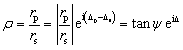 | (7) |
|
ε = ε1 + iε2 = sin2Φ{1 + [(1 − ρ)/(1 + ρ)]2tan2Φ}
| (8) |
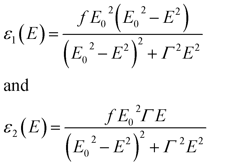 | (9) |
Fig. 8(a) and (b) shows ψ and Δ spectra of the MoS2 films fitted with the four-layered model described in the optical energy range of 1.5–3.5 eV. All the curves shows good fitting with average root means square error (RMSE) value ∼ 0.7. The ψ value of MoS2 films deposited for 15, 10 and 5 min increases in higher optical energy region while that of 1 and 2 min shows the opposite trend. The overall Δ increases with the increasing deposition time.
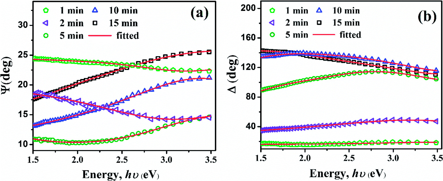 | ||
| Fig. 8 Plots of experimental and simulated SE parameters – (a) ψ and (b) Δ spectra of the MoS2 films fabricated for 1 to 15 min. | ||
The Bruggeman effective medium approximation (BEMA) model used for top layer of MoS2 films provides two parameters called the layer thickness (ds) and the fraction of the species (fv – 50%, fixed in our analysis). The value of ds is generally assumed to reflect the RMS roughness of the real surface. So far, there is no established straightforward relation between the RMS roughness, w and ds, obtained from AFM images and ellipsometric analysis of the thin films, respectively. A linear correlation between w and ds was estimated by Fujiwara et al. for a-Si:H films thought they also reported different w/ds ratios for different growth condition even for the same material.56,57 In case of self-affine surfaces, the BEMA roughness (ds) is given as the product of average surface slope (δ ∼ w/ξα) and the AFM surface roughness (ω), ds ∼ ωδ.58 The average surface slope is expected to remain constant for films following dynamic scaling. On the other hand for anomalous scaling δ is not constant but varies with time as δ ∼ tk, where k is a constant for a set of films deposited for different duration.59 The values of ds estimated from BEMA for MoS2 films fabricated at different deposition duration were not similar to that of w (Fig. 3(b)) for each film.
Fig. 9 exhibits the variation of ds as a function of w which shows that ds does not vary linearly with w and their slope (∼δ) also varies with time. The inset shows the log–log plot of δ vs. t where their slope k = 0.36 ± 0.04. The δ estimated from growth exponents (δ ∼ w/ξα) extracted from AFM analysis also scales with t as δ ∼ t0.43±0.01 which is close to that of estimated from slope of ds vs. w curve. The behavior of average local slope, δ ∼ t0.36±0.04, reconfirms presence of anomalous scaling of growth exponents during the PLD of the MoS2 films. Now, let us consider the SE analysis of main MoS2 layer, sandwiched between top roughness layer and the Corning glass substrate, for which a dispersion relation using four Lorentz oscillators was used. The thickness of the main MoS2 layer, estimated from SE analysis, were found to be ∼2.1, 5.5, 15.7, 37 and 77 nm for films deposited for 1, 2, 5, 10 and 15 min, respectively, which are similar to that measured from the profilometer.
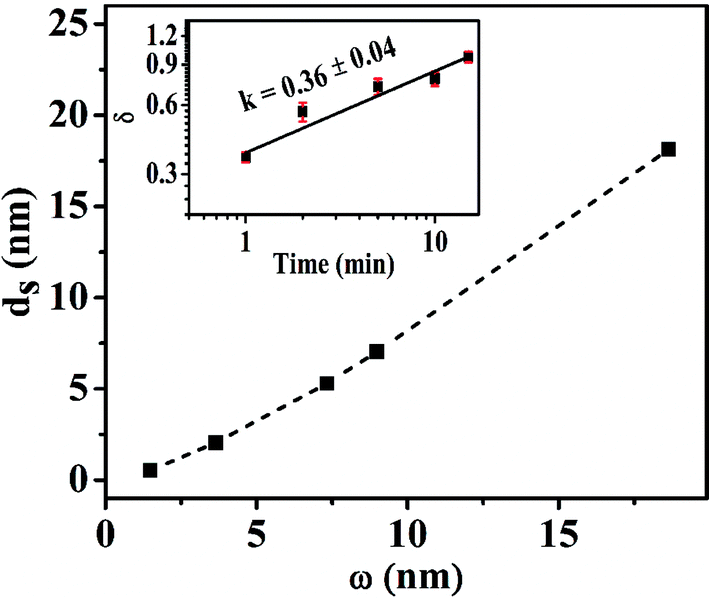 | ||
| Fig. 9 Plot of ds vs. w with an inset showing of δ vs. t in log–log scale. | ||
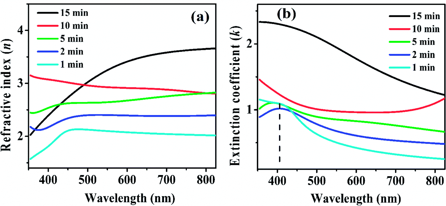
Fig. 10(a) and (b) shows the n and k spectra of the main MoS2 layer. Both refractive index (n) and extinction coefficient (k) spectra shows an overall increase with increasing deposition duration. The n and k spectra are nearly similar to that reported by Yim et al. for MoS2 films deposited on SiO2/Si substrate by vapor phase sulfurization process.60 The k spectra show absorption peak in the range of 2.8–3.3 eV corresponding to C/D excitonic transitions. ESI Fig. S3† exhibits variation of (a) amplitudes (f1, f2, f3 and f4) and (b) broadening parameters (Γ1, Γ2, Γ3 and Γ4) of four Lorentz oscillators, used to describe the dispersion law for the MoS2 film layer, as a function of deposition duration. For all the four oscillators their oscillator amplitude/strength were observed to increase with increasing deposition duration and thickness which is an indicative of formation of denser films at longer deposition times.55 Moreover, from AFM images (Fig. 2) it was observed that at early stage of film growth MoS2 clusters are sparsely distributed throughout the film but at longer deposition duration, densely packed larger clusters were formed. This morphology variation as a function of deposition duration is due to addition of new nucleation centers as well as continuous growth of already formed nuclei formed at early stages of film growth. The increase in coverage of film and cluster size (∼ξ) with increasing deposition duration results in decrease in void density and consequent increase in material density of film. From ESI Fig. S3(b),† a gradual decrease in broadening parameter was also observed with t. In our result, the correlation length (ξ) and crystalline grain size (shown by XRD analysis, ESI Fig. S1†) of the MoS2 films also grows with deposition time. Hence, the decline in Γ1, Γ2, Γ3 and Γ4 with t can be viewed as a result of increasing ξ (Fig. 3(c)). The result is quite similar to the reported decrease in broadening parameter with the grain size of polycrystalline and microcrystalline silicon thin films.61 The broadening of Lorentz oscillator is a consequence of surface scattering and lattice defect which represents the structural disorder in a sample. Thus, the reduction in Lorentz broadening parameter with growth time in the film indicates an increase in their structural order and hence enhancement in crystallinity of films was observed with increasing ξ. This enhanced structural order and crystallinity results in increased film compactness and density for thicker films. Now, considering similar layered model as above (depicted in ESI Fig. S4(a)†) and considering BEMA for middle layer (sandwiched between the top roughness layer and substrate) composed of voids and a MoS2 dispersion matrix, the void percentages within the films were estimated from SE data (details provided in ESI†).62 The void fraction present in the MoS2 films deposited for 1, 2, 5, 10 and 15 min are found to be 15.6, 14.1, 13.6, 8.8 and 6.0%, respectively, exhibiting decrease in void% with thickening of the film as depicted in ESI Fig. S4(b).†63 The increase in n with increasing deposition duration is due to increase in film density which is well supported by above observations. The increase in k with increasing deposition duration can also be explained as a result of an increase in the film density as well as their increasing RMS roughness. The increased surface roughness might have facilitated increased absorption due to increased surface area and enhanced light matter interaction due to local field effect. Hence both w and ξ seem to play a vital role in controlling the optical parameters of MoS2 films during their growth.
 | ||
| Fig. 10 Plots of (a) n and (b) k spectra of MoS2 films deposited for different time durations. | ||
4. Conclusions
In the present work, the kinetic roughening of MoS2 thin films grown by the PLD technique has been studied based on generic scaling ansatz using surface morphology information from AFM images of the films. The characteristic exponents αloc = 0.89 ± 0.05, α = 1.72 ± 0.11, αs = 0.85 ± 0.03, 1/z = 0.49 ± 0.11 and β = 0.85 ± 0.09 were determined using the HHCF and PSD functions. The local slope increases with growth time as, m ∼ tβ*. The value β* ∼ 0.41 ≠ 0 confirms that anomalous scaling has occurred. The anomalous scaling functions related to both HHCF and PSD for films deposited for different time periods collapsed to respective single curve confirming the presence of definite anomalous scaling during MoS2 film growth under PLD. These analyses revealed presence of intrinsic anomalous scaling of roughness with rapid roughening of the surfaces as αs < 1< α, αloc ∼ αs ≠ α. The growth exponents (αloc, β and 1/z) estimated in present case cannot be exactly related to any known universality classes based on both local and non-local growth models, suggesting that a different universality class needed to be defined. The models considering nonlocal effects like shadowing plays an important role in the evolution of growth front of these PLD thin films. The observed anomalous scaling behavior is also supported by the relation δ ∼ t0.36±0.04 extracted from SE studies. Moreover the SE studies also suggest that the optical functions (n and k) increases during film growth depending on the evolution of w and ξ with t as they control their surface area and the film density.Conflicts of interest
There are no conflicts of interest to declare.Acknowledgements
The authors acknowledged Department of Physics, IIT Guwahati for XRD facility, Center for Excellence in Nanoelectronics & Theranostic Devices, IIT Guwahati for AFM facility and CIF, IIT Guwahati for Raman and ellipsometer facilities. The authors gratefully acknowledge Mr Ankur Pandey for his kind help in AFM data recording.References
- X. Song, J. Hu and H. Zeng, J. Mater. Chem. C, 2013, 1, 2952–2969 RSC.
- Q. H. Wang, K. Kalantar-Zadeh, A. Kis, J. N. Coleman and M. S. Strano, Nat. Nanotechnol., 2012, 7, 699–712 CrossRef CAS PubMed.
- M. Xu, T. Liang, M. Shi and H. Chen, Chem. Rev., 2013, 113, 3766–3798 CrossRef CAS PubMed.
- K. F. Mak, C. Lee, J. Hone, J. Shan and T. F. Heinz, Phys. Rev. Lett., 2010, 105, 136805 CrossRef.
- A. Splendiani, L. Sun, Y. Zhang, T. Li, J. Kim, C.-Y. Chim, G. Galli and F. Wang, Nano Lett., 2010, 10, 1271–1275 CrossRef CAS PubMed.
- I. Song, C. Park and H. C. Choi, RSC Adv., 2015, 5, 7495–7514 RSC.
- Y. Yoon, K. Ganapathi and S. Salahuddin, Nano Lett., 2011, 11, 3768–3773 CrossRef CAS PubMed.
- L. Liu, S. B. Kumar, Y. Ouyang and J. Guo, IEEE Trans. Electron Devices, 2011, 58, 3042–3047 CAS.
- B. Radisavljevic, A. Radenovic, J. Brivio, V. Giacometti and A. Kis, Nat. Nanotechnol., 2011, 6, 147–150 CrossRef CAS.
- Y. Zhang, J. Ye, Y. Matsuhashi and Y. Iwasa, Nano Lett., 2012, 12, 1136–1140 CrossRef CAS PubMed.
- H. Qiu, L. Pan, Z. Yao, J. Li and Y. Shi, Appl. Phys. Lett., 2012, 100, 123104 CrossRef.
- Z. Yin, H. Li, H. Li, L. Jiang, Y. Shi, Y. Sun, G. Lu, Q. Zhang, X. Chen and H. Zhang, ACS Nano, 2011, 6, 74–80 CrossRef.
- H. Wang, L. Yu, Y.-H. Lee, Y. Shi, A. Hsu, M. L. Chin, L.-J. Li, M. Dubey, J. Kong and T. Palacios, Nano Lett., 2012, 12, 4674–4680 CrossRef CAS PubMed.
- J. Deng, W. Yuan, P. Ren, Y. Wang, D. Deng, Z. Zhang and X. Bao, RSC Adv., 2014, 4, 34733–34738 RSC.
- M. He, F. Kong, G. Yin, Z. Lv, X. Sun, H. Shi and B. Gao, RSC Adv., 2018, 8, 14369–14376 RSC.
- X. Chen, J. Ding, J. Jiang, G. Zhuang, Z. Zhang and P. Yang, RSC Adv., 2018, 8, 29488–29494 RSC.
- T. A. Loh and D. H. Chua, ACS Appl. Mater. Interfaces, 2014, 6, 15966–15971 CrossRef CAS PubMed.
- D. J. Late, P. A. Shaikh, R. Khare, R. V. Kashid, M. Chaudhary, M. A. More and S. B. Ogale, ACS Appl. Mater. Interfaces, 2014, 6, 15881–15888 CrossRef CAS PubMed.
- G. Nabiyouni and B. J. Farahani, Appl. Surf. Sci., 2009, 256, 674–682 CrossRef CAS.
- M. Al-Kuhaili, J. Phys. D: Appl. Phys., 2007, 40, 2847 CrossRef CAS.
- J. Jeffries, J.-K. Zuo and M. Craig, Phys. Rev. Lett., 1996, 76, 4931 CrossRef CAS PubMed.
- G. Palasantzas and J. Krim, Phys. Rev. Lett., 1994, 73, 3564 CrossRef CAS PubMed.
- M. Pelliccione, T. Karabacak, C. Gaire, G.-C. Wang and T.-M. Lu, Phys. Rev. B: Condens. Matter Mater. Phys., 2006, 74, 125420 CrossRef.
- G. Lengel, R. Phaneuf, E. Williams, S. D. Sarma, W. Beard and F. Johnson, Phys. Rev. B: Condens. Matter Mater. Phys., 1999, 60, R8469 CrossRef CAS.
- N. M. Das, D. Roy, N. Clarke, V. Ganesan and P. S. Gupta, RSC Adv., 2014, 4, 32490–32503 RSC.
- P. P. Chatraphorn, Z. Toroczkai and S. D. Sarma, Phys. Rev. B: Condens. Matter Mater. Phys., 2001, 64, 205407 CrossRef.
- A.-L. Barabási and H. E. Stanley, Fractal concepts in surface growth, Cambridge University Press, 1995 Search PubMed.
- Y. P. Zhao, J. Fortin, G. Bonvallet, G. C. Wang and T. M. Lu, Phys. Rev. Lett., 2000, 85, 3229 CrossRef CAS PubMed.
- A. R. Forouhi and I. Bloomer, Phys. Rev. B: Condens. Matter Mater. Phys., 1986, 34, 7018–7026 CrossRef CAS.
- S. Adachi, Phys. Rev. B: Condens. Matter Mater. Phys., 1988, 38, 12345–12352 CrossRef CAS.
- G. E. Jellison and F. A. Modine, Appl. Phys. Lett., 1996, 69, 371–373 CrossRef CAS.
- J. Tauc, R. Grigorovici and A. Vancu, Phys. Status Solidi B, 1966, 15, 627–637 CrossRef CAS.
- C. Lee, H. Yan, L. E. Brus, T. F. Heinz, J. Hone and S. Ryu, ACS Nano, 2010, 4, 2695–2700 CrossRef CAS PubMed.
- M. Ye, D. Winslow, D. Zhang, R. Pandey and Y. Yap, 2015.
- T. A. Loh and D. H. Chua, Chem. Phys. Lett., 2014, 610, 284–287 CrossRef.
- J. J. Ramasco, J. M. López and M. A. Rodríguez, Phys. Rev. Lett., 2000, 84, 2199–2202 CrossRef CAS PubMed.
- M. Pelliccione and T. M. Lu, Evolution of Thin Film Morphology: Modeling and Simulations, Springer-Verlag New York, New York, 1st edn, 2008 Search PubMed.
- K. L. Chopra, Thin Film Phenomena, McGraw-Hill Book Company, New York, 1969 Search PubMed.
- M. Nasehnejad, G. Nabiyouni and M. G. Shahraki, J. Phys. D: Appl. Phys., 2017, 50, 375301 CrossRef.
- I. Gupta and B. C. Mohanty, Sci. Rep., 2016, 6, 33136 CrossRef CAS PubMed.
- M. Saitou, Phys. Rev. B: Condens. Matter Mater. Phys., 2002, 66, 073416 CrossRef.
- S. Das Sarma, C. J. Lanczycki, R. Kotlyar and S. V. Ghaisas, Phys. Rev. E: Stat., Nonlinear, Soft Matter Phys., 1996, 53, 359–388 CrossRef CAS.
- J. M. López, M. A. Rodríguez and R. Cuerno, Phys. Rev. E: Stat., Nonlinear, Soft Matter Phys., 1997, 56, 3993–3998 CrossRef.
- J. M. López, Phys. Rev. Lett., 1999, 83, 4594–4597 CrossRef.
- S. M. Obaidulla and P. Giri, Appl. Phys. Lett., 2015, 107, 221910 CrossRef.
- M. F. Torres and R. C. Buceta, Eur. Phys. J. B, 2013, 86, 20 CrossRef CAS.
- W. W. Mullins, J. Appl. Phys., 1957, 28, 333–339 CrossRef CAS.
- S. F. Edwards and D. R. Wilkinson, Proc. R. Soc. London, Ser. A, 1982, 381, 17–31 CrossRef.
- M. Kardar, G. Parisi and Y.-C. Zhang, Phys. Rev. Lett., 1986, 56, 889 CrossRef CAS PubMed.
- J. M. López, M. Castro and R. Gallego, Phys. Rev. Lett., 2005, 94, 166103 CrossRef PubMed.
- J. H. Yao and H. Guo, Phys. Rev. E: Stat. Phys., Plasmas, Fluids, Relat. Interdiscip. Top., 1993, 47, 1007 CrossRef.
- R. Karunasiri, R. Bruinsma and J. Rudnick, Phys. Rev. Lett., 1989, 62, 788 CrossRef PubMed.
- J. T. Drotar, Y.-P. Zhao, T.-M. Lu and G.-C. Wang, Phys. Rev. B: Condens. Matter Mater. Phys., 2000, 62, 2118 CrossRef CAS.
- I. Weaver and C. Lewis, J. Appl. Phys., 1996, 79, 7216–7222 CrossRef CAS.
- H. Fujiwara, Spectroscopic ellipsometry: principles and applications, John Wiley & Sons, 2007 Search PubMed.
- H. Fujiwara, M. Kondo and A. Matsuda, Phys. Rev. B: Condens. Matter Mater. Phys., 2001, 63, 115306 CrossRef.
- H. Fujiwara, J. Koh, P. Rovira and R. Collins, Phys. Rev. B: Condens. Matter Mater. Phys., 2000, 61, 10832 CrossRef CAS.
- M. Losurdo and K. Hingerl, Ellipsometry at the Nanoscale, Springer, 2013 Search PubMed.
- G. Palasantzas, Phys. Rev. E: Stat. Phys., Plasmas, Fluids, Relat. Interdiscip. Top., 1997, 56, 1254 CrossRef CAS.
- C. Yim, M. O'Brien, N. McEvoy, S. Winters, I. Mirza, J. G. Lunney and G. S. Duesberg, Appl. Phys. Lett., 2014, 104, 103114 CrossRef.
- S. Logothetidis, J. Appl. Phys., 1989, 65, 2416–2426 CrossRef CAS.
- P. McMarr, J. Blanco, K. Vedam, R. Messier and L. Pilione, Appl. Phys. Lett., 1986, 49, 328–330 CrossRef CAS.
- S. T. Sundari, S. Dash and A. Tyagi, presented in part at International Conference on Nanoscience, Engineering and Technology (ICONSET 2011), Chennai, November, 2011 Search PubMed.
Footnotes |
| † Electronic supplementary information (ESI) available. See DOI: 10.1039/c9ra01867k |
| ‡ Equal contribution. |
| This journal is © The Royal Society of Chemistry 2019 |