
 Open Access Article
 This Open Access Article is licensed under a Creative Commons Attribution-Non Commercial 3.0 Unported Licence
Interface depended electronic and magnetic properties of vertical CrI3/WSe2 heterostructures
Mei Geab,
Yan Su c,
Han Wangd,
Guohui Yangb and
Junfeng Zhang*b
c,
Han Wangd,
Guohui Yangb and
Junfeng Zhang*b
aSchool of Physics and Information Engineering, Shanxi Normal University, Linfen, 041004, China
bKey Laboratory of Spectral Measurement and Analysis of Shanxi Province, Shanxi Normal University, Linfen, 041004, China. E-mail: zhangjf@sxnu.edu.cn
cKey Laboratory of Materials Modification by Laser, Ion and Electron Beams, Dalian University of Technology, Ministry of Education, Dalian 116024, China
dChemical Sciences Division, Lawrence Berkeley National Laboratory, Berkeley, California 94720, USA
First published on 14th May 2019
Abstract
Owing to the great potential applications in information processing and storage, two-dimensional (2D) magnetic materials have recently attracted significant attention. Here, using first-principles calculations, we investigate the electronic and magnetic properties of the van der Waals CrI3/WSe2 heterostructures. We find that after forming heterostructures, monolayer CrI3 undergoes a direct to indirect band gap transition and its gap size is greatly reduced. In particular, the out-plane spin quantization axis of monolayer CrI3 is tuned into in-plane for most stacking configurations of CrI3/WSe2. We further reveal that the transition of the easy magnetization direction is mainly originated from the hybridization between Cr-d and Se-p orbitals. These theoretical results provide a useful picture for the electronic structure and magnetic anisotropy behaviors in vertical CrI3/WSe2 heterostructures.
Introduction
As triggered by graphene,1,2 two-dimensional (2D) materials such as hexagonal BN3 and transition metal dichalcogenides (TMDs),4,5 have become the focus of intensive studies during the past decade because of their unique properties and the great promise for novel applications. Among them, materials with long-range ferromagnetic order are most desirable for applications in spintronics devices.6 However, most 2D materials in their pristine forms are intrinsically nonmagnetic, and the magnetic moments introduced by dopants, defects, edges, or coupling to ferromagnetic substrates7 are mostly very local. Therefore, the recently fabricated 2D intrinsic ferromagnetic materials, such as chromium germanium telluride (Cr2Ge2Te6 (ref. 8)), CrI3 (ref. 9) and VSe2,10 have attracted much attention for the promised applications as high-density magnetic memories and spintronic applications at the nanoscale.CrI3 is layered van der Waals material with order ferromagnetically, the Curie temperature (Tc) is 61 K for bulk11–14 and 45 K for monolayer.9 Monolayer CrI3 is a semiconductor9,15 with the band gap of 1.2 eV.16–18 By including spin–orbit coupling (SOC), the band gap will decrease to 0.9 eV.16,18 The magnetism arises from the partially filled d orbitals of the Cr3+ ion, and the magnetocrystalline anisotropy favours an out-plane spin orientation.12 It has been demonstrated that the magnetic properties of CrI3 can be controlled by strain,19–23 electric fields24–28 and magnetic fields.21,29
To combine the advantages of two different 2D materials, stacking them into a heterostructure has been proven to be an effective way.30,31 Until now, many kinds of 2D heterostructures have been fabricated successfully in experiments,32–34 and their physical properties have been predicated theoretically.35–39 For magnetic materials, it is known that they can be integrated with many other materials, including conductors40 and semiconductors.41 Recently, increasing attention has been paid to the 2D ferromagnetic heterostructures. For example, by the electrostatic doping in CrI3/graphene heterostructures, Jiang et al. found that the saturation magnetization can be tuned up to 40% experimentally.25 A theoretical study16 on CrI3/graphene heterostructure indicated that a Chern insulating state can be achieved. Moreover, it is possible to control the spin and valley pseudospin properties of WSe2 by constructing CrI3/WSe2 ferromagnetic heterostructure.42,43 However, some questions still need to be answered. For example, what are the interfacial (stacking type) effects on the electronic and magnetic properties of this kinds of heterostructures? Is it possible to tune the magnetic anisotropy energy (MAE) in CrI3/WSe2 heterostructures?
In this paper, by using first principle calculations, we report the interface effects on the electronic structure and magnetic properties in 2D ferromagnetic CrI3/WSe2 heterostructures. We consider three different stacking types for both bilayer and triple layer vertical heterostructures. The tuneable band gap and magnetic properties can be found and understood with the help of orbital hybridization and SOC effects.
Computational methods
The structural and electronic properties of monolayer CrI3, bilayer and triple layer CrI3/WSe2 heterostructures were computed using the DFT and projector-augmented wave method (PAW)44 implemented in the VASP code.45 The Perdew–Burke–Ernzerhof (PBE) functional46 was used to describe the exchange–correction interaction. The plane wave basis was expanded up to a cutoff energy 550 eV. Grimme's semiempirical DFT-D3 scheme for dispersion correction47 was employed to describe the van der Waals (vdW) interactions between the CrI3 and the WSe2 layers. In the direction perpendicular to the sheet, 5 nm thickness was selected to avoid any spurious interaction with the image sheets. For each configuration, the atomic coordinates and in-plane supercell parameters were fully relaxed, until the Hellmann–Feynman force on each atom became smaller than 0.01 eV Å−1 and the total energy was converged to be within 10−6 eV. The 2D Brillouin zones were sampled by an 14 × 14 × 1 k-point grid mesh.48 Spin polarization was taken into the account, and the effect of SOC was also introduced for the calculations of the electric properties. In addition, to include the interactions between 3d orbits of Cr atoms, the DFT+U methods described by Dudarev49 were used. Here, in the electronic calculations, the on-site Coulomb parameter (U) and the exchange parameter (J) were selected as U = 2.7 eV and J = 0.7 eV,17,18 respectively.Results and discussion
As shown in Fig. 1a, monolayer CrI3 is a I–Cr–I sandwich structure where each Cr is surrounded by six first neighboring I atoms. In the Cr atomic layer, the Cr atoms form a honeycomb lattice. Owing to the octahedral symmetry, the five d-orbitals (dxy, dxz, dyz, dx2−y2, dz2) of Cr are split into three half-filled t2g orbitals and two empty eg orbitals.17 The magnetization comes directly from the honeycomb Cr lattice. The orbital configuration of the I− ion (5s25p6) has a very strong SOC, which results in antisymmetric exchange effects and anisotropic symmetric exchange effects.17 In Fig. 2, we show the band structures of monolayer CrI3 without and with SOC, where the direct band gaps are 1.05 eV and 0.72 eV, respectively. These results are consistent with previous DFT calculations.16–18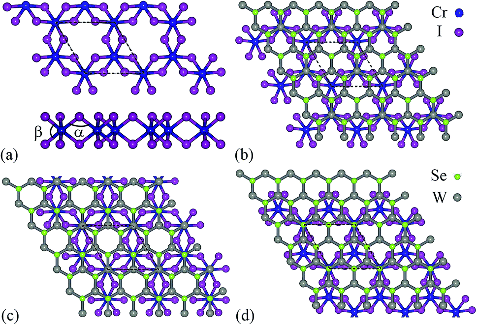 | ||
| Fig. 1 The structure model for (a) monolayer CrI3 (upper: top view, lower: side view), and (b–d) CrI3/WSe2 heterostructures with different stacking way ((b) Se-site, (c) top-site and (d) W-site). | ||
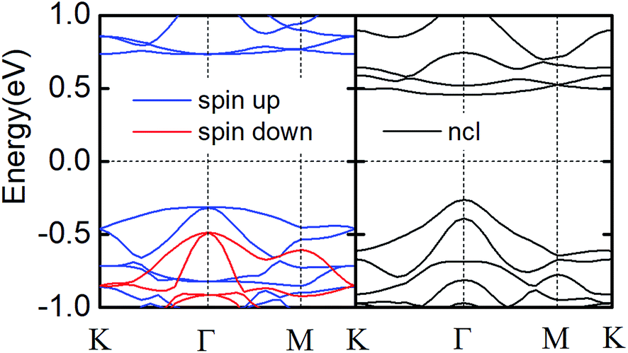 | ||
| Fig. 2 Band structure of monolayer CrI3 without (left panel) and with (right panel) SOC. | ||
We discuss here the bilayer CrI3/WSe2 and trilayer WSe2/CrI3/WSe2 heterostructures. For monolayer CrI3 and WSe2, the optimized lattice parameter is 7.002 Å and 3.321 Å, respectively. In bilayer CrI3/WSe2 heterostructure, monolayer CrI3 (1 × 1) stacked on monolayer WSe2 (2 × 2) vertically. The trilayer WSe2/CrI3/WSe2 heterostructure has a sandwich structure, in which the monolayer CrI3 (1 × 1) is surrounded by two layers of WSe2 (2 × 2). Therefore, the lattice mismatch between CrI3 (1 × 1) and WSe2 (2 × 2) is about 5.42%. In both bilayer and triple layer heterostructures, the lattice parameter of adopted that of CrI3 lattice (7.002 Å), and the WSe2 layer has been enlarged uniformly. As shown in Fig. 1b–d, three kinds of vertical stacking types have been considered in the present calculation, bi-Se, bi-T and bi-W for bilayer heterostructures. For bi-Se CrI3/WSe2 heterostructure, as shown in Fig. 1b, only one Cr atom is located on the top of a W atom in a unit cell. Similarly, for the bi-W configuration, one Cr atom is located on the top of a I2 pair in a unit cell (see Fig. 1d). For the bi-T configuration as shown in Fig. 1c, one Cr atom is located on the top of W atom, and the other Cr atom located on the top of I2 atom. In the trilayer WSe2/CrI3/WSe2 heterostructures, the CrI3/WSe2 stacking in tri-Se, tri-T and tri-W configurations are similar to those in bi-Se, bi-T and bi-W configurations, and the two WSe2 layers are stacked by the AA type.
As can be seen from the data in Table 1, the bi-Se (tri-Se) stacking type is the most favourite configuration in the bilayer (trilayer) heterostructures, which is 6.33 (23.19) and 85.40 (18.76) meV per cell more stable than bi-T (tri-T) and bi-W (tri-W). Meanwhile, the -Se configuration also has the shortest interlayer distance (0.6654 nm for bi-Se, 0.6667 nm for tri-Se), compared with those of -T (0.6674 nm for bi-T and 0.6668 nm for tri-T) and -W (0.6685 nm for bi-W and 0.6842 for tri-W) configurations. Even so, it is noted that the energy differences between different stacking configurations are relatively small and their interlayer distances are comparable, suggesting the superlubricity in the vertical CrI3/WSe2 heterostructures, which has been found in bilayer graphene.50 Moreover, the Bader charger analysis51 suggests that, the -Se configurations have less inter-layer charge transfer (0.009 electrons per cell for bi-Se, and 0.007 electrons per cell for tri-Se) than -T and -W configurations. The electronic properties and magnetic properties of CrI3 are known to rely on its structural properties. Fig. 3 shows that, the distribution of the bond length (Cr–I, Lbond) and bond angels (α: ∠I–Cr–I, β: ∠Cr–I–Cr as labelled in Fig. 1a) of CrI3 in monolayer (black dots), bilayer (left panel) and trilayer (right panel) heterostructures. For the case of monolayer CrI3, according to our calculation, the lattice constant, Lbond, α and β are 7.002 Å, 2.737 Å, 90.6° and 94.5° (84.8°), respectively. These results are consistent with previous theoretical results.12,13,19,24 When forming CrI3/WSe2 heterostructures, the inter-layer van de Waals interaction makes both the bond length and the bond angles of CrI3 slightly changed. As shown in Fig. 3, the bond information of CrI3 in bi-Se and tri-Se are closer with the monolayer case, which are responsible for the lower formation energy indicated in Table 1. Nevertheless, both the bond angle and bond length have been interrupted by the WSe2 layer in bilayer and triple layer CrI3/WSe2 heterostructures. The bond angle of α and β accounts the ferromagnetic superexchange symmetry.24 Therefore, the electronic properties and magnetic properties of CrI3 in heterostructure are supposed to be different from those of monolayer CrI3.
| Er | d | Q | |
|---|---|---|---|
| Bi-Se | 0 | 0.6654 | 0.009 |
| Bi-T | 6.33 | 0.6674 | 0.012 |
| Bi-W | 85.40 | 0.6685 | 0.014 |
| Tri-Se | 0 | 0.6667 | 0.007 |
| Tri-T | 23.19 | 0.6668 | 0.015 |
| Tri-W | 18.76 | 0.6842 | 0.023 |
 | ||
| Fig. 3 Bond length (Lbond) and bond angle (α and β) for bilayer and tri-layer CrI3/WSe2 heterostructures with three different stacking models. | ||
We then next discuss the electronic and magnetic properties of the CrI3/WSe2 heterostructures. When stacked into heterostructure, as shown in Fig. 4 for bilayer and Fig. 5 for triple layer CrI3/WSe2 heterostructures, the band structure of CrI3 depends on the interlayer interactions. Firstly, we can also see from the band structures is that, the band alignment in both bilayer and triple layer CrI3/WSe2 heterostructures can be categorized into staggered type (type-II). Secondly, compared with the band gap of monolayer CrI3 (see Fig. 2), i.e., 1.05 eV (without SOC) and 0.72 eV (with SOC), band gap of CrI3 in heterostructures is larger. Without (with) SOC, band gap of CrI3 in bilayer heterostructures is 1.13 (1.12), 1.13 (1.07) and 1.19 (0.90) eV for bi-Se, bi-T and bi-W, respectively. For trilayer CrI3/WSe2 heterostructures, the band gaps without (with) SOC are 1.07 (1.07) eV for tri-Se, 1.07 (1.04) eV for tri-T and 0.96 (1.01) eV for tri-W, respectively (see Fig. 5). Thirdly, the direct-to-indirect band gap transition can be found from monolayer CrI3 to CrI3/WSe2 heterostructures. For monolayer CrI3, either with or without SOC (see Fig. 2), the band gap is direct. However, for both bilayer and triple layer CrI3/WSe2 heterostructures, the interlayer interaction tuned the band gap to indirect (without considering SOC). When considering the SOC, tri-Se still have indirect band gap, in which the valence band maximum (VBM) is located at Γ point, but the conduction band minimum (CBM) is located at K point (see Fig. 5). As shown in Fig. 4 and 5, less than 0.1 eV energy difference at different K points in the flat conductance bands. Then, it is easier to switch between the direct band gap and indirect one by using different interlayer interactions. It is found that the CBM is contributed by Cr, I and W atoms, then the SOC effect mainly resulting from I− atoms is one reason for the direct to indirect change.
 | ||
| Fig. 4 Band structure of bilayer CrI3/WSe2 heterostructures without (a–c) and with (d–f) SOC for bi-Se (a and d), bi-T (b and e) and bi-W (c and f) stackings. The grey lines are band of the heterostructure, and stars are band mainly contributed from CrI3 layer. The bandgap is indirect without SOC, but tuned direct for bi-T and bi-W stackings after the SOC have been considered. | ||
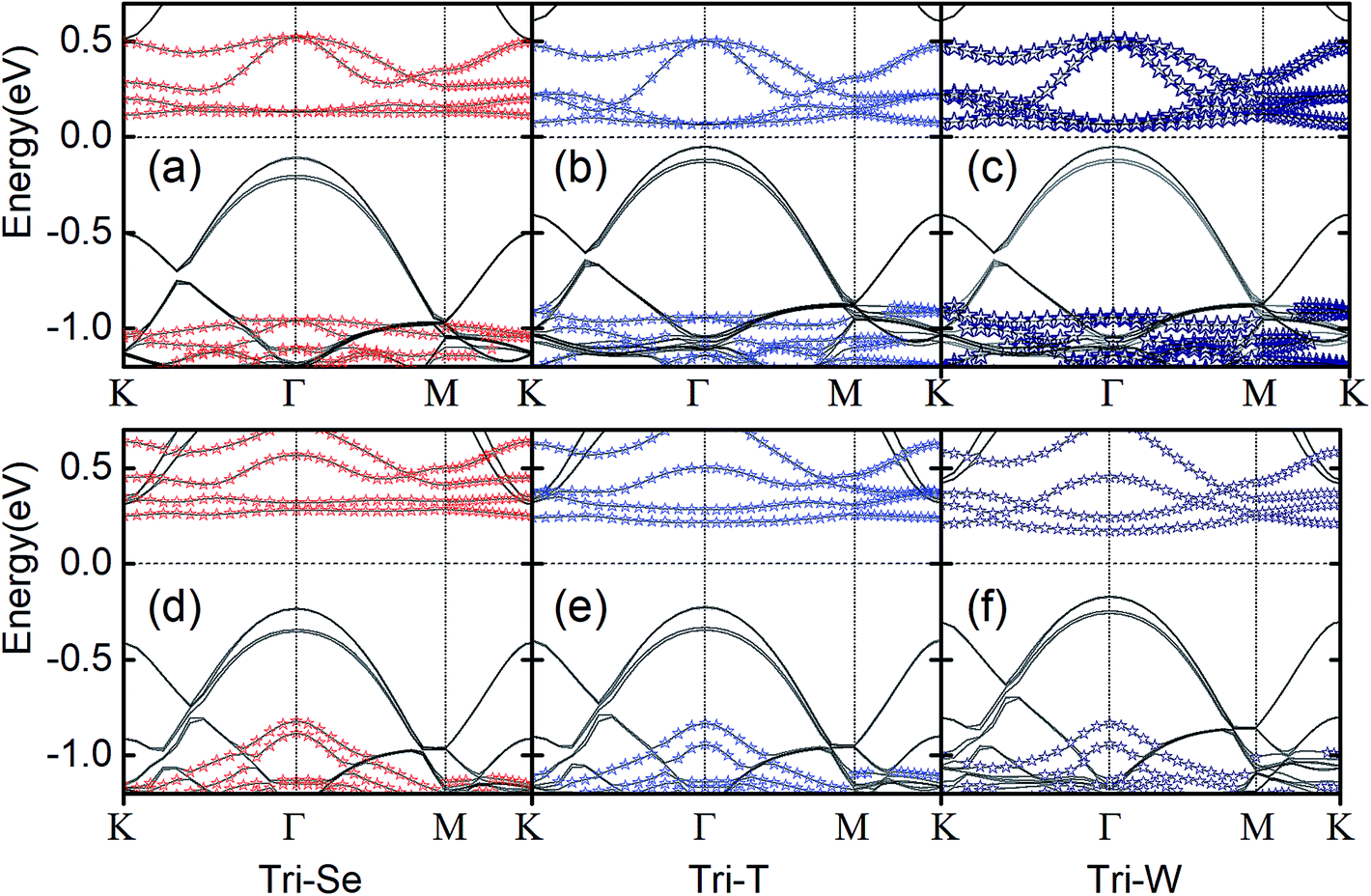 | ||
| Fig. 5 Band structure of triple layer CrI3/WSe2 heterostructures without (a–c) and with (d–f) SOC for tri-Se (a and d), tri-T (b and e) and tri-W (c and f) stackings. The grey lines are band of the heterostructure, and stars are band mainly contributed from CrI3 layer. | ||
Magnetic anisotropy originating mainly from SOC effects,17,30 is an important parameter when it comes to 2D magnets as it is qualitatively related to their magnetic stability. MAE is defined as the difference between energies corresponding to the magnetization in the in-plane and out-plane directions (MAE = Em//a − Em//c), in which Em//a is the energy for the in-plane magnetization, and Em//c is the energy for the out-plane magnetization. A positive (negative) value of MAE indicated the out-plane (in-plane) easy axis. Taking SOC effects into account, the total energies Em//a and Em//c can be achieved through noncollinear calculations, and then the MAE can be evaluated. Consistent with the previous calculations12,18,19,21 and experimental results,13,17 because of the strong SOC in the heavier iodine ions,17 the easy axis for monolayer CrI3 is out-plane with MAE 0.73 meV per Cr atom.
One most interesting finding is that, as shown in Table 2, the out-plane easy axis in monolayer CrI3 changed into in-plane in CrI3/WSe2 heterostructures with almost all kinds of stacking types. The only exception is tri-T, which is still out-plane easy axis with MAE 0.03 meV per Cr. Remarkable large MAE can be found for the most stable stacking configurations in both bilayer and triple layer CrI3/WSe2 heterostructures, i.e., 0.17 meV per Cr and 0.23 meV per Cr for bi-Se and tri-Se, respectively.
| -Se | -T | -W | |
|---|---|---|---|
| Monolayer | Out-plane (0.73) | ||
| Bi | In-plane (−0.17) | In-plane (−0.03) | In-plane (−0.02) |
| Tri | In-plane (−0.23) | Out-plane (0.03) | In-plane (−0.04) |
Noteworthy, the charge transfer in bilayer heterostructures (see Table 1) can result in a net dipole moment. With the dipole correction, our calculation indicated that the MAE and magnetic moment can be changed about 0.001 meV per Cr and 0.001 μB per Cr, respectively. In Fig. 6a, take bi-Se CrI3/WSe2 heterostructures as an example, we compared the wave function characteristics at the G point Cr d and Se pz orbits between out-plane and in-plane easy axis. It can be seen clearly that, the hybridizations take placed between Cr_dxz,yz, Cr_dz2 and Se_pz orbits, as the results of the interlayer interaction between CrI3 layer and WSe2 layer. This should responsible for the easy axis transition in CrI3/WSe2 heterostructures as suggested in Fe/MgO interfaces.52 The only exception is the tri-T CrI3/WSe2 heterostructure, in which the out-plane easy axis is maintained. Therefore, except for applying the in-plane external magnetic field,18 we demonstrated here that the spin direction can be shifted from out-plane to in-plane by stacking with the WSe2 layer. The easy axis direction should be another reason for the direct-to-indirect band gap transition. We calculated the band structures for bi-Se CrI3/WSe2 heterostructure with two different magnetic moment orientations (m//a and m//c) as shown in Fig. 6b. For m//a, the CBM located at K point, but the VBM is located at Γ point, which makes the band gap indirect. For m//c, however, both the CBM and VBM located at Γ point, then the band gap is direct. Moreover, it can be also found in Fig. 6b and 4a, both the CBM and VBM are degenerated at Γ point for m//a and without SOC. It is known that, the CBM at Γ point is mainly results from px and py orbitals of I atom.18 When the SOC is included and with the out-plane easy axis, the energy split for VBM and CBM at Γ point. Therefore, the transition of easy axis from out-plane to in-plane is one reason for the direct-to-indirect band gap switch.
 | ||
| Fig. 6 (a) Effects of spin axis on the wave function characteristics at G points for Cr d and Se pz orbitals for bi-Se CrI3/WSe2 heterostructures. (b) Band structure of bi-Se CrI3/WSe2 heterostructures for the magnetic moment along the in-plane a axis (left panel) out-of-plane c axis (right panel). The arrows show that the bandgap is indirect with m//a and direct with m//c. | ||
Conclusions
To summarize, our first-principles calculations unveil the effect of interfaces on the electronic and magnetic properties of vertical CrI3/WSe2 heterostructures. We find that the -Se stacking is the most stable configuration in either bilayer or triple layer CrI3/WSe2 heterostructures. The switch between direct and indirect band gap can be found mainly because of the SOC effects of the p orbits of I atoms. Most importantly, originated from hybridizations between d orbits of Cr atoms and p orbital of Se atoms, the easy axis transition from the out-plane of monolayer CrI3 to in-plane for almost all stacking type of both bilayer and triple layer CrI3/WSe2 heterostructures is found. All these theoretical results constitute a useful picture of vertical CrI3/WSe2 heterostructures for the interface effect on the electronic and magnetic behaviors and provide vital guidance in designing novel spintronic 2D devices.Conflicts of interest
There are no conflicts to declare.Acknowledgements
This work was supported by the National Natural Science Foundation of China (11674046) and the Scientific and Technological Innovation Programs of Higher Education Institutions in Shanxi (201802070).Notes and references
- A. K. Geim and K. S. Novoselov, Nat. Mater., 2007, 6, 183 CrossRef CAS PubMed.
- K. S. Novoselov, A. K. Geim, S. V. Morozov, D. Jiang, Y. Zhang, S. V. Dubonos, I. V. Grigorieva and A. A. Firsov, Science, 2004, 306, 666–669 CrossRef CAS PubMed.
- Y. Kubota, K. Watanabe, O. Tsuda and T. Taniguchi, Science, 2007, 317, 932–934 CrossRef CAS PubMed.
- H. Fang, S. Chuang, T. C. Chang, K. Takei, T. Takahashi and A. Javey, Nano Lett., 2012, 12, 3788–3792 CrossRef CAS PubMed.
- K. F. Mak, C. Lee, J. Hone, J. Shan and T. F. Heinz, Phys. Rev. Lett., 2010, 105, 136805 CrossRef PubMed.
- G. A. Prinz, Science, 1998, 282, 1660 CrossRef CAS PubMed.
- W. Han, R. K. Kawakami, M. Gmitra and J. Fabian, Nat. Nanotechnol., 2014, 9, 794 CrossRef CAS PubMed.
- C. Gong, L. Li, Z. Li, H. Ji, A. Stern, Y. Xia, T. Cao, W. Bao, C. Wang, Y. Wang, Z. Q. Qiu, R. J. Cava, S. G. Louie, J. Xia and X. Zhang, Nature, 2017, 546, 265 CrossRef CAS PubMed.
- B. Huang, G. Clark, E. Navarro-Moratalla, D. R. Klein, R. Cheng, K. L. Seyler, D. Zhong, E. Schmidgall, M. A. McGuire, D. H. Cobden, W. Yao, D. Xiao, P. Jarillo-Herrero and X. Xu, Nature, 2017, 546, 270 CrossRef CAS PubMed.
- M. Bonilla, S. Kolekar, Y. Ma, H. C. Diaz, V. Kalappattil, R. Das, T. Eggers, H. R. Gutierrez, M.-H. Phan and M. Batzill, Nat. Nanotechnol., 2018, 13, 289–293 CrossRef CAS PubMed.
- J. F. Dillon Jr and C. E. Olson, J. Appl. Phys., 1965, 36, 1259–1260 CrossRef.
- W.-B. Zhang, Q. Qu, P. Zhu and C.-H. Lam, J. Mater. Chem. C, 2015, 3, 12457–12468 RSC.
- M. A. McGuire, H. Dixit, V. R. Cooper and B. C. Sales, Chem. Mater., 2015, 27, 612–620 CrossRef CAS.
- L. Chen, J.-H. Chung, B. Gao, T. Chen, M. B. Stone, A. I. Kolesnikov, Q. Huang and P. Dai, Phys. Rev. X, 2018, 8, 041028 CAS.
- C. Lee, F. Katmis, P. Jarillo-Herrero, J. S. Moodera and N. Gedik, Nat. Commun., 2016, 7, 12014 CrossRef CAS PubMed.
- J. Zhang, B. Zhao, T. Zhou, Y. Xue, C. Ma and Z. Yang, Phys. Rev. B, 2018, 97, 085401 CrossRef CAS.
- J. L. Lado and J. Fernández-Rossier, 2D Materials, 2017, 4, 035002 CrossRef.
- P. Jiang, L. Li, Z. Liao, Y. X. Zhao and Z. Zhong, Nano Lett., 2018, 18, 3844–3849 CrossRef CAS PubMed.
- L. Webster and J.-A. Yan, Phys. Rev. B, 2018, 98, 144411 CrossRef CAS.
- F. Iyikanat, M. Yagmurcukardes, R. T. Senger and H. Sahin, J. Mater. Chem. C, 2018, 6, 2019–2025 RSC.
- G. Guo, G. Bi, C. Cai and H. Wu, J. Phys.: Condens. Matter, 2018, 30, 285303 CrossRef PubMed.
- F. Zheng, J. Zhao, Z. Liu, M. Li, M. Zhou, S. Zhang and P. Zhang, Nanoscale, 2018, 10, 14298–14303 RSC.
- Z. Wu, J. Yu and S. Yuan, Phys. Chem. Chem. Phys., 2019, 21, 7750–7755 RSC.
- J. Liu, M. Shi, J. Lu and M. P. Anantram, Phys. Rev. B, 2018, 97, 054416 CrossRef CAS.
- S. Jiang, L. Li, Z. Wang, K. F. Mak and J. Shan, Nat. Nanotechnol., 2018, 13, 549–553 CrossRef CAS PubMed.
- B. Huang, G. Clark, D. R. Klein, D. MacNeill, E. Navarro-Moratalla, K. L. Seyler, N. Wilson, M. A. McGuire, D. H. Cobden, D. Xiao, W. Yao, P. Jarillo-Herrero and X. Xu, Nat. Nanotechnol., 2018, 13, 544–548 CrossRef CAS PubMed.
- N. Sivadas, S. Okamoto, X. Xu, C. J. Fennie and D. Xiao, Nano Lett., 2018, 18, 7658–7664 CrossRef CAS PubMed.
- M. U. Farooq and J. Hong, NPJ. 2D Mater. Appl., 2019, 3, 3 CrossRef.
- Z. Wang, I. Gutiérrez-Lezama, N. Ubrig, M. Kroner, M. Gibertini, T. Taniguchi, K. Watanabe, A. Imamoğlu, E. Giannini and A. F. Morpurgo, Nat. Commun., 2018, 9, 2516 CrossRef PubMed.
- A. K. Geim and I. V. Grigorieva, Nature, 2013, 499, 419 CrossRef CAS PubMed.
- Y. Liu, N. O. Weiss, X. Duan, H.-C. Cheng, Y. Huang and X. Duan, Nat. Rev. Mater., 2016, 1, 16042 CrossRef CAS.
- M. P. Levendorf, C.-J. Kim, L. Brown, P. Y. Huang, R. W. Havener, D. A. Muller and J. Park, Nature, 2012, 488, 627 CrossRef CAS PubMed.
- Y. Gong, J. Lin, X. Wang, G. Shi, S. Lei, Z. Lin, X. Zou, G. Ye, R. Vajtai, B. I. Yakobson, H. Terrones, M. Terrones, B. K. Tay, J. Lou, S. T. Pantelides, Z. Liu, W. Zhou and P. M. Ajayan, Nat. Mater., 2014, 13, 1135 CrossRef CAS PubMed.
- M.-Y. Li, Y. Shi, C.-C. Cheng, L.-S. Lu, Y.-C. Lin, H.-L. Tang, M.-L. Tsai, C.-W. Chu, K.-H. Wei, J.-H. He, W.-H. Chang, K. Suenaga and L.-J. Li, Science, 2015, 349, 524–528 CrossRef CAS PubMed.
- J. Zhang, W. Xie, J. Zhao and S. Zhang, 2D Materials, 2016, 4, 015038 CrossRef.
- J. Zhang, W. Xie, M. L. Agiorgousis, D.-H. Choe, V. Meunier, X. Xu, J. Zhao and S. Zhang, Nanoscale, 2018, 10, 7912–7917 RSC.
- K. D. Pham, N. N. Hieu, H. V. Phuc, B. D. Hoi, V. V. Ilysov, B. Amin and C. V. Nguyen, Comput. Mater. Sci., 2018, 153, 438–444 CrossRef CAS.
- P. T. T. Le, L. M. Bui, N. N. Hieu, H. V. Phuc, B. Amin, N. V. Hieu and C. V. Nguyen, Diamond Relat. Mater., 2019, 94, 129–136 CrossRef CAS.
- K. D. Pham, N. N. Hieu, H. V. Phuc, I. A. Fedorov, C. A. Duque, B. Amin and C. V. Nguyen, Appl. Phys. Lett., 2018, 113, 171605 CrossRef.
- A. I. Buzdin, Rev. Mod. Phys., 2005, 77, 935–976 CrossRef CAS.
- A. H. MacDonald, P. Schiffer and N. Samarth, Nat. Mater., 2005, 4, 195 CrossRef CAS.
- D. Zhong, K. L. Seyler, X. Linpeng, R. Cheng, N. Sivadas, B. Huang, E. Schmidgall, T. Taniguchi, K. Watanabe, M. A. McGuire, W. Yao, D. Xiao, K.-M. C. Fu and X. Xu, Sci. Adv., 2017, 3, e1603113 CrossRef PubMed.
- K. L. Seyler, D. Zhong, B. Huang, X. Linpeng, N. P. Wilson, T. Taniguchi, K. Watanabe, W. Yao, D. Xiao, M. A. McGuire, K.-M. C. Fu and X. Xu, Nano Lett., 2018, 18, 3823–3828 CrossRef CAS PubMed.
- G. Kresse and D. Joubert, Phys Rev B, 1999, 59, 1758–1775 CrossRef CAS.
- G. Kresse and J. Furthmüller, Comput. Mater. Sci., 1996, 6, 15–50 CrossRef CAS.
- J. P. Perdew, K. Burke and M. Ernzerhof, Phys. Rev. Lett., 1996, 77, 3865–3868 CrossRef CAS PubMed.
- S. Grimme, J. Antony, S. Ehrlich and H. Krieg, J. Chem. Phys., 2010, 132, 154104 CrossRef PubMed.
- H. J. Monkhorst and J. D. Pack, Phys. Rev. B: Solid State, 1976, 13, 5188–5192 CrossRef.
- S. L. Dudarev, G. A. Botton, S. Y. Savrasov, C. J. Humphreys and A. P. Sutton, Phys. Rev. B: Condens. Matter Mater. Phys., 1998, 57, 1505–1509 CrossRef CAS.
- M. Dienwiebel, G. S. Verhoeven, N. Pradeep, J. W. M. Frenken, J. A. Heimberg and H. W. Zandbergen, Phys. Rev. Lett., 2004, 92, 126101 CrossRef PubMed.
- G. Henkelman, A. Arnaldsson and H. Jónsson, Comput. Mater. Sci., 2006, 36, 354–360 CrossRef.
- H. X. Yang, M. Chshiev, B. Dieny, J. H. Lee, A. Manchon and K. H. Shin, Phys. Rev. B: Condens. Matter Mater. Phys., 2011, 84, 054401 CrossRef.
| This journal is © The Royal Society of Chemistry 2019 |