
 Open Access Article
 This Open Access Article is licensed under a Creative Commons Attribution-Non Commercial 3.0 Unported Licence
Strong Volta potential change in doped zinc oxide as a photoresponse to UV irradiation
Silvia Huber ab,
Cezarina Cela Mardareab,
Andrei Ionut Mardareb,
Christoph Kleberb and
Achim Walter Hassel*ab
ab,
Cezarina Cela Mardareab,
Andrei Ionut Mardareb,
Christoph Kleberb and
Achim Walter Hassel*ab
aChristian Doppler Laboratory for Combinatorial Oxide Chemistry at the Institute for Chemical Technology of Inorganic Materials (TIM), Johannes Kepler University Linz, Altenberger Str. 69, 4040 Linz, Austria
bTIM, Johannes Kepler University Linz, Altenberger Str. 69, 4040 Linz, Austria. E-mail: achimwalter.hassel@elchem.de
First published on 1st November 2019
Abstract
Doped ZnO thin films on ITO substrates were prepared by reactive co-sputtering of ZnO and several dopant metals, namely Al, Mn, Ti, W or Zr. To elucidate the influence of the dopant, morphological and compositional investigations were performed applying SEM/EDX, XRD and AFM. The optical band gaps of the materials were determined by UV-VIS measurements and the subsequent analysis of the derived Tauc plots. SKP (Scanning Kelvin Probe) measurements were performed under alternating illumination periods in order to measure the CPD (contact potential difference) response on UV irradiation; effective donor concentrations were calculated from the SKP results. The obtained X-ray diffractograms revealed that W![[thin space (1/6-em)]](https://www.rsc.org/images/entities/char_2009.gif) :ZnO is amorphous, whereas all other dopants form crystalline structures with diffraction angles shifted towards lower values. SEM and AFM imaging revealed a significant influence of the dopant on the film morphology. The optical band gap values are in the range of the ZnO value (∼3.30 eV), with the lowest value of 3.29 eV being measured for Mn:ZnO. An exception was found for W:ZnO, which exhibits significant band gap widening reaching 4.35 eV. The effective donor concentrations are low for all samples under dark conditions, whereas they showed enhanced values under illumination. The sensitivity of all materials towards illumination makes them promising candidates for future research activities in the field of photovoltaics.
:ZnO is amorphous, whereas all other dopants form crystalline structures with diffraction angles shifted towards lower values. SEM and AFM imaging revealed a significant influence of the dopant on the film morphology. The optical band gap values are in the range of the ZnO value (∼3.30 eV), with the lowest value of 3.29 eV being measured for Mn:ZnO. An exception was found for W:ZnO, which exhibits significant band gap widening reaching 4.35 eV. The effective donor concentrations are low for all samples under dark conditions, whereas they showed enhanced values under illumination. The sensitivity of all materials towards illumination makes them promising candidates for future research activities in the field of photovoltaics.
1. Introduction
The upsurge of solar energy use is unprecedented and it has already reached a wide mass of private customers. It is also extensively utilized in industry as part of power grids to enable them to operate self-sufficiently in times of higher energy demand. Yet there are still some unsolved issues related to efficiency, material costs, stability and the storage of energy. ZnO is a very promising candidate to solve several of these issues, due to the fact that other materials suffer from high costs, shortages and toxicity.1,2 Although this material is highly researched, several new approaches have emerged recently in order to answer unsolved questions regarding energy production/storage.3 As green technology, photoelectrochemical water splitting is a hot topic due to the almost inexhaustible sources of the basic material and the environmentally friendly process. ZnO superstructures have thereby exhibited remarkable results in this research field.4 One of the most important properties is flexibility of the ZnO to form nanostructures in almost every imaginable shape. For example, arrays of ZnO nanowires showed good piezoelectric properties and are able to form a nanogenerator.5 The latest findings have proved their usability in biosensors6 and photodetectors, which are used e.g. for wearable devices.7Amorphous ZnO films have recently gained attention from the scientific community8 due to their potential application for thin film transistors.9,10 Concerning this topic, there is still a lack of basic knowledge about the properties of amorphous ZnO materials due to the fact that it is challenging to synthesize them in stable forms. Theoretical calculations predict enhanced stability for doped amorphous ZnO.8 As we have previously successfully fabricated amorphous W:ZnO on a glass substrate,11 the aim here was to produce this amorphous layer on ITO-coated substrates and to evaluate the resulting optoelectronic and morphological properties. The chosen doping concentration of W is based on the findings from DFT calculations in ref. 12. The aim was to achieve a doping of around 2 at% W, which was shown by the authors to form a stable state due to the presence of WZn. Furthermore, W-doping with the formation of WZn was suggested to decrease the bandgap in the direction of the visible region of the spectrum. For lower concentrations of W, it can be expected that the films tend to crystallise as suggested by ref. 13 and 14.
Additionally, other doping materials (Mn, Ti, Zr and Al) were considered in this work due to the promising results obtained in previous investigations.15–19 It was shown before that an ITO buffer layer may act as an effective electron collector and enhance the photocatalytic activity of a material.20 Therefore, the aim of this work was to perform a comparative study of the optoelectronic and morphological differences of various doped ZnO thin films in the context of the resulting structures on ITO substrates. In order to perform a comparative study where the effect of certain dopants is to be analysed, the total dopant concentration should be kept at a constant level. Yim et al. established a detailed database of single-element doped ZnO via first-principles calculations. They assumed a constant dopant concentration of around 0.2 at% for comparing the different doping elements.21 Referring to this study, it was decided to keep the doping concentration at low values in order to examine the influence of the doping element without it being predominant due to a too high concentration. Subsequently, the doping concentrations of Mn, Ti, Zr and Al were chosen to be below 0.4 at% allowing us to compare the influence of these dopants with respect to the mentioned properties.
In addition, the effect of illumination on the CPD (also called the Volta potential) has been determined, as well as the optical bandgaps of the doped ZnO layers on the ITO-coated substrates. The charge carrier concentration has already been successfully quantified via Scanning Kelvin Probe-Force Microscopy (SKP-FM).22 Here, a conventional SKP was used. Due to the fact that the basic principle is the same for both techniques, the determination of the charge carrier concentration is possible also with the conventional SKP and could be successfully demonstrated in this study.
2. Methods
2.1. Sample preparation
The ITO substrates (ITO coated glass 30B, 30 Ω □−1, Visiontek System Ltd., United Kingdom) were cleaned ultrasonically in acetone and isopropanol, followed by drying in nitrogen flow. All thin films were prepared by reactive co-sputtering of ZnO and the individual dopant of interest (Al, Mn, Ti, W, or Zr). A schematic drawing of the experimental set-up for the preparation is given elsewhere,11 and Fig. 1 depicts schematically the obtained layer structure. The distance between the targets and the substrate is 130 mm, the total process time is 2.5 hours, and the power density for the ZnO target is 3.70 W cm−2 for all depositions, while for the doping element 1.23 W cm−2 is used. All depositions were carried out at 0.5 Pa, and the base pressure in the process chamber was approximately 10−5 to 10−6 Pa. Reactive sputtering was performed in a mixture of Ar and O2. O2 and Ar flows were precisely controlled during the whole process and set to 41 ± 1 sccm for Ar and 2 ± 0.5 sccm for O2. The substrates were rotated at 5 rpm to ensure uniform film thicknesses.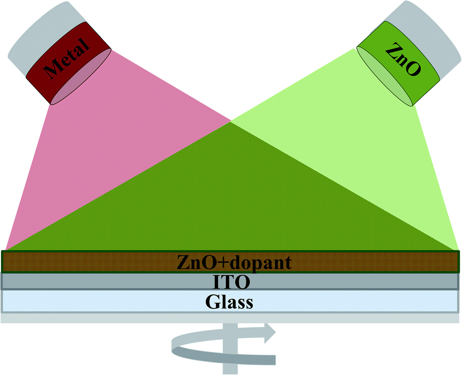 | ||
| Fig. 1 Schematic drawing of the doped ZnO/ITO system. | ||
2.2. Sample characterization
The obtained film thicknesses were measured by profilometry (Bruker DekTakXT), and crystallographic analysis was performed with a Philips X'Pert Pro X-ray Diffraction (XRD) system using Cu Kα-radiation with Bragg–Brentano geometry. For the analysis and phase identification, X'Pert High Score Plus software with the PDF 2 database was used. Surface imaging was done with a Zeiss 1540-XB field emission scanning electron microscope (FE-SEM) at an acceleration voltage of 20 kV. The elemental quantification was performed via an in-built energy dispersive X-ray spectrometer (EDX) from INCA X-Sight Oxford Instruments. The compositional resolution of the system was empirically determined using alloys with defined composition. EDX errors are in the range of 0.1 at% at stable vacuum levels, meaning that a final reported compositional resolution of 1 at% may be provided with 10% error. Atomic force microscopy (AFM) investigations of the surfaces were accomplished using a Nanosurf Easyscan 2 system and the data visualization was done by Gwyddion 2.45 software. UV-VIS measurements were performed with a UV-1800 spectrophotometer from Shimadzu in the scanning range of 250–700 nm. This system delivered the absorption (A) as the measurement result for each of the materials under study. From these values, Tauc plots were derived and the optical band gaps (Eg) of the materials could be calculated. Details with respect to the formulas used, as well as their derivation and coherences, are provided elsewhere.11 SKP measurements were performed using an in-house developed chamber containing the SKP measurement head (Wicinski–Wicinski GbR) and an x–y motorized sample table. The chamber is equipped with a temperature, atmosphere and humidity stabilization system. Additionally, an illumination unit with a constant wavelength of 365 nm (Thorlabs, Germany, M365D2), controlled by a Thorlabs DC2200 LED driver, was installed in order to enable SKP measurements under illumination. The measured power density was 56 mW cm−2. All measurements were done at an average probe-sample distance of about 75 μm and a vibration frequency of approximately 1 kHz. Ambient temperature was held constant at 25 ± 0.5 °C and the humidity at 3 ± 0.5%. The SKP probe was a Ni tip with a diameter of 210 μm. Calibration was done by using a Cu/CuSO4 (saturated) system prior to each measurement. The obtained Volta potential values are given with reference to the standard hydrogen electrode (SHE). All measurements were carried out at single points (without surface scanning) with 10 minutes on/off illumination cycling for a total measurement time of 130 minutes and a contact potential difference (CPD) time resolution of 5 s. An influence of the probe material (needle of the SKP) itself on the results can be excluded due to the fact that it was proven in previous measurements that there is no influence of the UV-irradiation.The surface photovoltage (SPV) can be measured by the SKP method.23 The SPV and the CPD are related to each other as -eΔSPV = eΔCPD.24,25
| ΔCPD = CPDdark − CPDilluminated | (1) |
As it can be seen from eqn (1), the SPV is simply defined by the difference of the CPDs when the sample is illuminated, or measured in the dark, respectively. For the determination of the ΔCPD in this study, the differences between the very first on/off cycles under illumination were used. To simplify the analysis, the measurements were carried out under illumination at a fixed wavelength of 365 nm, which is close to the expected band gap of the thin films.
Besides the ΔCPD, another important property of the materials can be determined via SKP measurements – the charge carrier density. Maragliano et al. successfully quantified the charge carrier concentration in ZnO thin films by SKP-FM measurements.22 As the principles of SKP-FM and SKP are in general the same, eqn (2) is applied to the present measurement results in order to derive the respective effective donor concentrations (CD) of the doped and pristine ZnO thin films. The carrier density is given as:
 | (2) |
3. Results and discussion
A final thickness of 264 ± 5 nm for the pristine ZnO was measured by contact profilometry and the dopant concentrations were quantified by EDX. Table 1 summarizes the obtained values.| Dopant | Doping concentration/at% | Film thickness/nm |
|---|---|---|
| Al | 0.3 ± 0.1 | 259 ± 5 |
| Mn | 0.1 ± 0.1 | 208 ± 5 |
| W | 3.5 ± 0.1 | 250 ± 6 |
| Ti | 0.4 ± 0.1 | 271 ± 3 |
| Zr | 0.4 ± 0.1 | 237 ± 6 |
3.1. XRD-measurements
The X-ray diffractograms are depicted in Fig. 2a and b. Miller indices of the ZnO reference pattern (PDF-2 No. 01-080-0075) diffraction peaks are written above the obtained XRD results for the pristine ZnO. Additionally, a plot of dashed lines of the ZnO main peaks was inserted for comparison purposes across all other patterns. The pattern of the pristine ZnO thin film is in good agreement with the reference pattern. This proves the crystallinity of the as-deposited thin film. As described in previous studies of doped ZnO deposited on glass substrates, W as a dopant severely disrupts the atomic structure of ZnO resulting in the formation of an amorphous layer.11 The same effect is found in the current study for W:ZnO deposited on ITO. Al:ZnO has a very similar diffraction pattern to the pristine ZnO, whereas the (002) peaks of Ti, Mn and Zr doped ZnO (in ascending order) are shifted towards lower diffraction angles. Concomitant with the (002) peak shift, the preferential orientation of the coatings in the [002] direction becomes increasingly evident, with the disappearance of other additional reflections and relative increase in the (002) peak intensity (not emphasized in the plot). A peak shift towards lower angles occurs when elements with higher ionic radii substitutionally replace the Zn2+ ions. All doping elements used in this study have smaller ionic radii, with the exception of Al. Consequently, the shift should have been towards higher 2θ angles. In the case where foreign atoms are incorporated into interstitial sites and not as substitutional ions instead of Zn2+, a peak shift toward lower angles was reported.11,27 Detailed studies performed on Al-doped ZnO demonstrated that Al is found in both substitutional and interstitial sites,28,29 whereas Ti is found as interstitial.27 The atomic radii of the dopants (206 pm for Zr, 193 pm for W, 176 pm for Ti and 161 pm for Mn) are all larger than that of Zn (135 pm), with the exception of Al (118 pm). Therefore, it can be inferred that Mn, Ti, Zr and W doping elements occupy interstitial positions in the ZnO matrix. According to these findings, the magnitude of the peak shift as a function of different elements is related to both the size of the atomic radius of the dopant and the concentration.
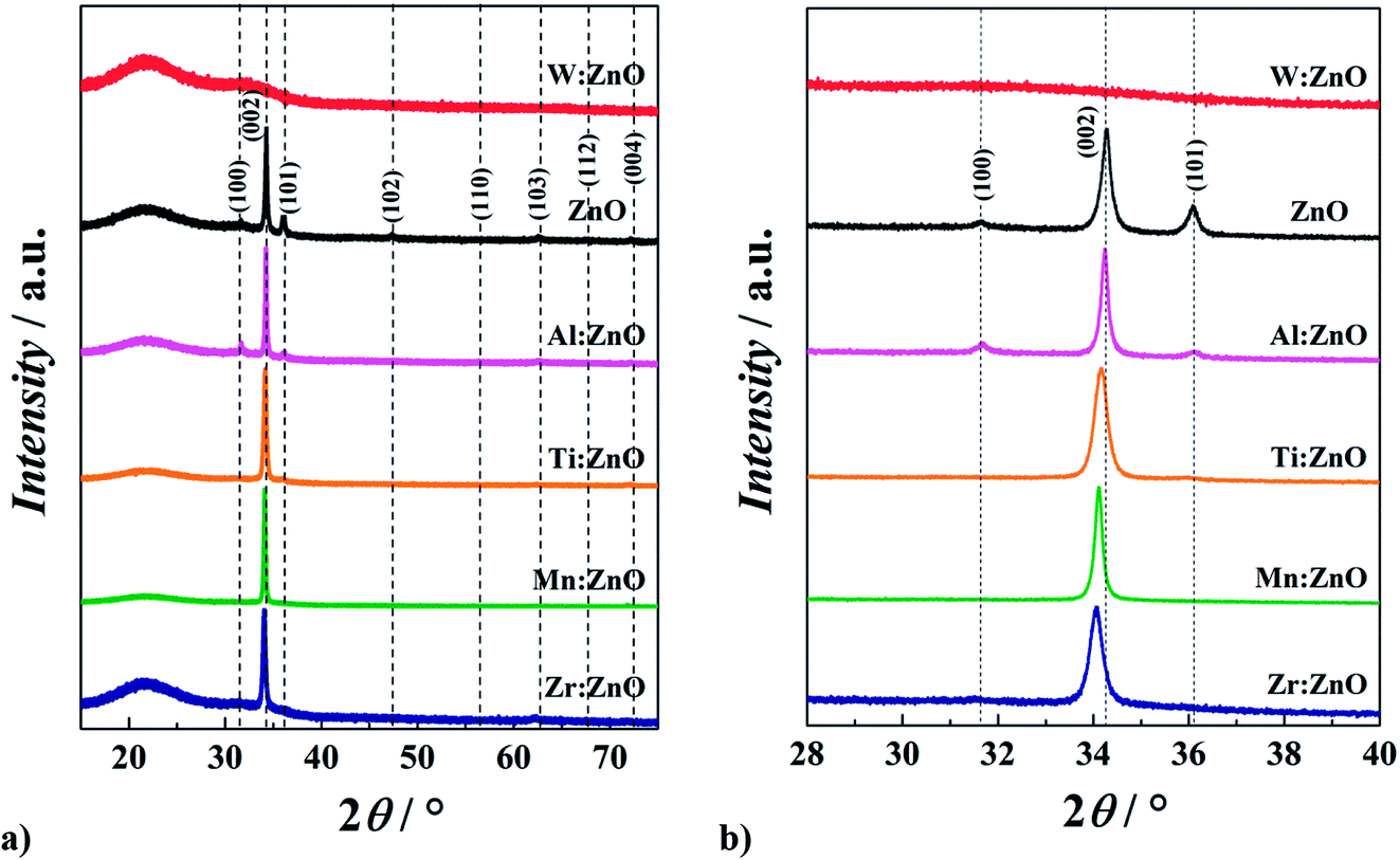 | ||
| Fig. 2 XRD patterns of doped and pristine ZnO thin films: (a) for diffraction angles between 15 and 75° and (b) a higher resolution zoomed-in plot for diffraction angles ranging from 28 to 40°. | ||
Slightly different results are obtained for Zr:ZnO films, showing the largest shift towards lower 2θ, but there seems to be less preferential orientation as evidenced by the presence of the (103) peak.
For this sample, also the relative intensity of the (002) reflection is decreased as compared to other doped-ZnO films. This indicates a possible initiation of amorphization caused by the extremely large atomic radius of Zr (206 pm) as compared to Zn (135 pm). Even though it has an atomic radius larger than the atomic radius of W (193 pm), Zr does not lead to complete amorphization of ZnO, most probably due to its much lower concentration as compared to W.
Based on the peak positions and Miller indices, the lattice parameters (a and c) were also calculated in order to gain insight into the influence of doping elements onto the resulting ZnO structure (Table 2). As compared to pure ZnO, all doping elements trigger the expansion of the unit cell, especially by increasing the value of the c parameter due to the larger atomic radius. Al doping has nearly no effect on the lattice parameter values, whereas Ti addition leads to the expansion of both a and c due to its much larger atomic radius. The extremely highly textured Mn:ZnO films show only the (002) reflection, and therefore only the calculation of the c parameter was possible. Zr doping led to an increase in the c parameter, whereas the a value was lower than for pristine ZnO.
| Sample name | Lattice parameter/Å | |
|---|---|---|
| a | c | |
| ZnO | 3.260 | 5.228 |
| Al:ZnO |
3.256 | 5.234 |
| Ti:ZnO |
3.497 | 5.245 |
| Mn:ZnO |
— | 5.253 |
| Zr:ZnO |
3.244 | 5.260 |
3.2. SEM measurements
Morphological investigations acquired by SEM imaging are presented in Fig. 3. ITO has a very fine structure, with the grains in the range of 10 nm. Pristine ZnO has grains in a broad size range from roughly 20 to 70 nm. It can be clearly seen that all doping elements have an influence on the obtained surface morphology. Ti and Mn doped ZnO thin films are rather similar, and both refine the structure of the layer, leading to grains as large as 60 nm. Al:ZnO has slightly larger grains than pristine ZnO, with the grains up to 100 nm and a much more open surface morphology. Doping ZnO with Zr leads to a different structure containing large grains of the same size as for pristine ZnO, but consisting of much smaller crystallites with a size of around 10 nm. It can be concluded that this structure is a result of the epitaxial growth of the Zr:ZnO crystals on the ITO substrate, which can also be found on the pristine ZnO layer even though it is not so pronounced. All other doping elements do not show this epitaxial growth behaviour. W:ZnO has a very smooth morphology with isolated single large grains with the size of 100 nm (which are suspected to originate from the underlying ITO substrate), confirming the amorphous character of the coating proven by XRD.
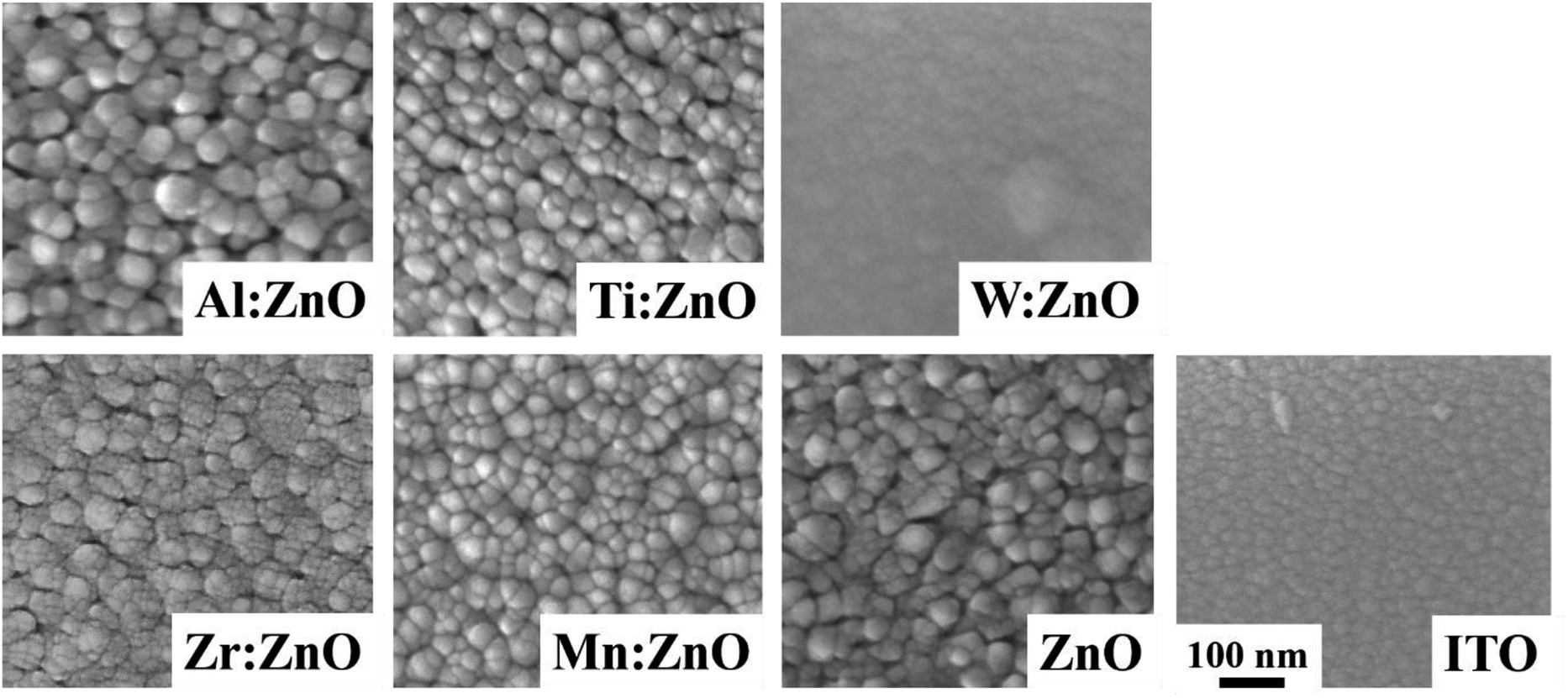 | ||
| Fig. 3 SEM images of pristine ZnO, the ITO substrate without coating and doped ZnO. The scale is valid for all images. | ||
3.3. AFM-measurements
3-D AFM height profiles of a 1 × 1 μm2 surface scan are shown in Fig. 4. These corroborate in general the findings of the SEM imaging. The topographies of the pristine ZnO, Zr:ZnO and Al:ZnO appear rougher than for the other samples. It can be seen that Al:ZnO exhibits larger grains compared to the other doped layers, especially W:ZnO and Mn:ZnO, which have a smoother surface. Some occasional appearance of larger grains can be seen on the ITO as well on the W:ZnO.
 | ||
| Fig. 4 3D-AFM profile images (1 × 1 μm2) of pristine ZnO, uncoated ITO substrate and doped ZnO films. | ||
This optical appearance is also quantitatively confirmed in terms of Ra and Rms values obtained from the topographic information provided by the AFM mappings. A summary of these results is illustrated in Fig. 5, with dashed lines marking the values for undoped ZnO. Pristine ZnO has the highest roughness values, showing also the highest difference between Ra and Rms. This is evidence of this sample having a larger number of spikes and pits and consequently its higher roughness than all of the other doped samples due to the higher sensitivity of the Rms towards height deviations. W:ZnO exhibits the lowest roughness, which is due to its amorphous structure. From the crystalline samples, Mn:ZnO is the one with the lowest roughness and smoothest surface followed by Al:ZnO, Ti:ZnO, and Zr:ZnO, in ascending order.
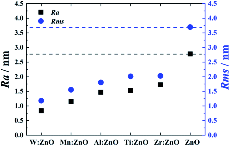 | ||
| Fig. 5 Roughness parameters for (un)doped-ZnO in terms of Ra and Rms values. Dashed lines indicate the values of pristine ZnO. | ||
3.4. UV-VIS-measurements
The obtained UV-VIS absorbance spectra are shown in Fig. 6. All samples show fluctuating absorbance in the visible region above 400 nm. This enhanced Fabry–Pérot interference may originate from the ITO on the glass substrate and the superimposed layer causing the light to undergo multiple reflections at the front- and backside of the samples.30 Uncoated ITO has also been investigated by UV-VIS but showed no absorbance in the wavelength range of interest. The absorption edges of all samples except W:ZnO start at around 390 nm and are very similar for Al, Mn, Zr, and Ti doped and pristine ZnO. For W:ZnO, the absorption edge is much lower, with a starting point of 350 nm. Mn:ZnO shows a red shift and W:ZnO a blue shift, which is also the case when the samples are deposited on glass substrates but at lower wavelengths.11
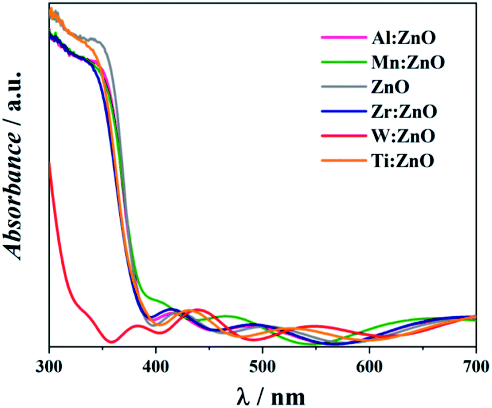 | ||
| Fig. 6 UV-VIS absorbance spectra of doped and pristine ZnO films on an ITO substrate. | ||
Tauc plots were calculated from the absorbance spectra in order to obtain the values for the optical band gaps, Eg. The plots themselves and the intersections of the tangents for the determination of Eg are presented in Fig. 7. The corresponding obtained values for Eg are presented in Table 3. For better visibility, the plot of W:ZnO is presented as an inset in Fig. 7. The optical band gap of pristine ZnO is at 3.31 eV. It can be clearly seen that Mn:ZnO has a lower band gap than pristine ZnO and all other doped ZnO thin films because it absorbs at a lower energy value. This is in good agreement with the results of the SKP measurements, which were accomplished under illumination with 365 nm UV-light (Section 3.5). Previous studies of Mn doped ZnO also proved a red shift in the band gap. This makes Mn:ZnO a highly promising candidate for further photocatalytic research activities.16 W:ZnO shows the highest Eg value, while Zr and Ti doped films exhibit slightly higher optical band gaps than pristine ZnO. The Eg of Al:ZnO is the only one that is the same as that for undoped ZnO. The effect of band gap blue-shifting may be attributed to the Burstein–Moss effect,31 which was already observed in previous studies of doped ZnO films.19,32,33
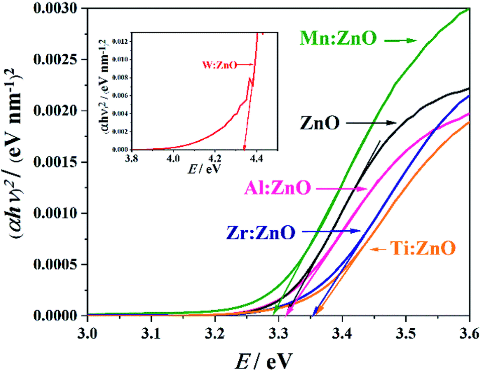 | ||
| Fig. 7 Band gap determination via Tauc plots of doped and pristine ZnO films on an ITO substrate. W:ZnO is shown as an inset to enable better visibility of both graphs. | ||
| Sample | Optical band gap Eg/eV |
|---|---|
| Mn:ZnO |
3.29 |
| ZnO | 3.31 |
| Al:ZnO |
3.31 |
| Zr:ZnO |
3.35 |
| Ti:ZnO |
3.35 |
| W:ZnO |
4.35 |
3.5. SKP-measurements
SKP measurements with 10 minutes automated on/off illumination cycling are shown in Fig. 8. The yellow background marks periods with illumination. The samples have different initial values of the Volta potential due to their differences in work function. All layers show a strong response of the CPD upon UV-illumination, except for W:ZnO whose absorption edge is located at a lower wavelength. Because of this fact, there was no significant influence of illumination on the CPD of W:ZnO and therefore it was omitted from the graph. Illumination of all other materials including the blank ITO-coated substrate led to a significant Volta potential drop in the range of several hundreds of mV. The absorption of photons with an energy above or close enough to the conduction band leads to the generation of electron–hole pairs, directly affecting the potential at the sample surface.24 Even though recombination occurs very fast (in less than 1 s), the continuous photon absorption leads to a stationary regime when the CPD remains at a constant level until the illumination is switched off. It may be expected that this enhanced photoresponsivity is due to the combination of the underlying ITO and the superimposed (doped) ZnO layer. The substrate itself was also analysed and showed a significant potential drop in the range of 100 mV in the first few seconds followed by a further attenuated drop until the end of the illumination period. The fact that the work function of ITO is higher than 4.2 eV (the values differ in the literature but are shown to be higher than 4.5 eV,34 with the newest studies reporting values around 5 eV35) justifies why there was no absorption in the UV-VIS range (as previously discussed). The response of its Volta potential to irradiation with 365 nm light may be related to sub-bandgap transitions due to defects or surface states.24 It is noticeable that once illuminated, the CPD of the ITO does not recover even after switching off the light again.
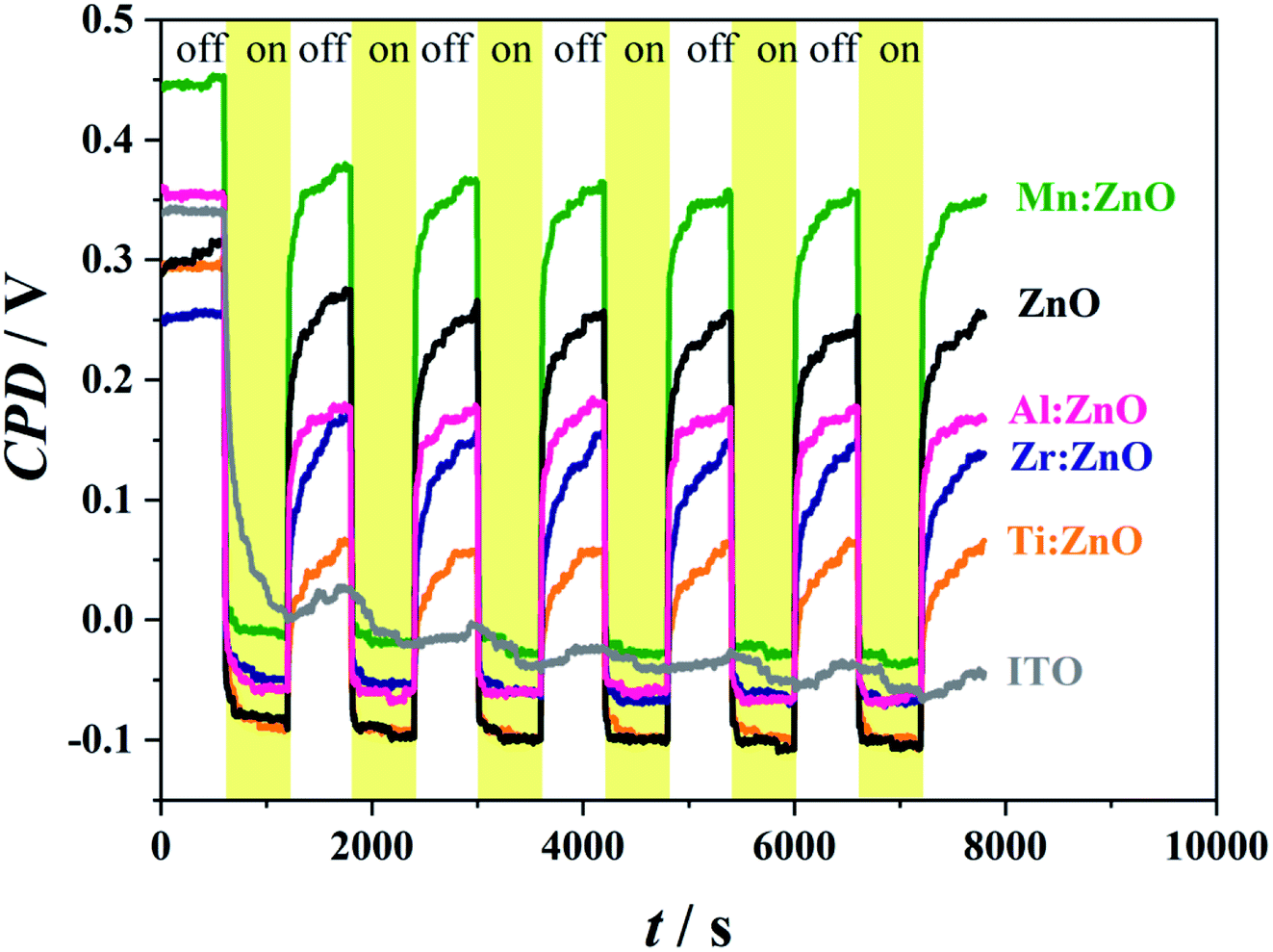 | ||
| Fig. 8 SKP measurement results of doped and pristine ZnO thin films and uncoated ITO shown for comparison purposes. Yellow background indicates periods with illumination switched on. Time of on/off cycle: 10 min; total measurement time: 130 min. | ||
Mn doped ZnO exhibits the highest potential drop of 430 mV, whereas Zr:ZnO shows the lowest one (260 mV). It is remarkable that there is a fast Volta potential recovery after switching off the light, followed by a slow increase of the CPD after the first seconds of the dark period. This behaviour is similar to the CPD drop during the illumination period and could be related to bulk effects. The hindering of the recovery of the Volta potential may be due to slow recombination processes involving surface states36 and/or delayed charge transfer through the bulk of the film for photons absorbed deeper inside the material.37
The recombination triggering the CPD increase is the fastest for Mn:ZnO and the slowest for Ti:ZnO and Zr:ZnO. In general, the response is similar for each cycle and there are no charge accumulating phenomena occurring as experimentally observable in Fig. 8 through potential plateaus. The charge carrier activation/recombination is fully reversible for all samples except for ITO. The fast response on UV illumination is an interesting property for all tested doped and pristine ZnO thin films on an ITO buffer layer, even though the Volta potential change occurs as a two-step process (a fast-surface states and a slow-bulk one). This agrees well with previous studies where the fast process is attributed to the photogeneration of electron–hole pairs. Electrons are accumulating in the bulk, whereas holes are gathered on the surface, screening negatively charged surface states. This leads to physisorbed oxygen (from the atmosphere) becoming chemisorbed due to electrons travelling from the bulk to the surface.38 The absence of an effective hole collector on top (like (doped) ZnO) may explain the very slow recovery of the ITO's CPD in the dark.
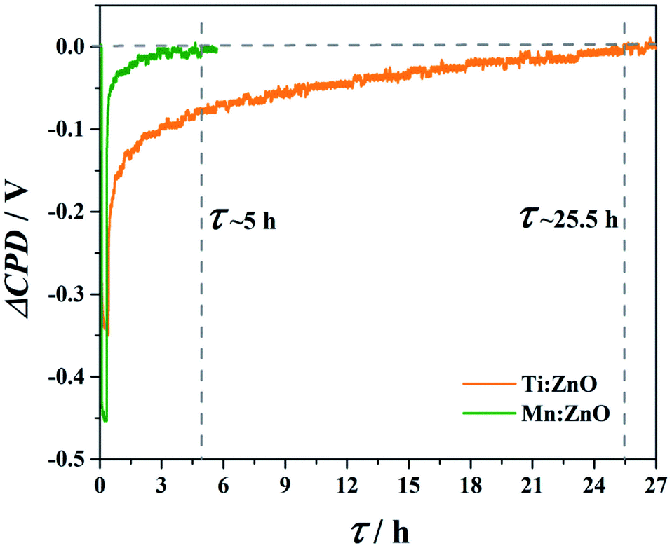
The relaxation time τ is defined as the time dependent change in the SPV after switching off the illumination.39 For illustrating different relaxation times, transient SPV measurements were performed for all doped ZnO materials. Due to better visibility and to demonstrate two extremes of the relaxation time, in Fig. 9 are plotted the SPV transients of Mn:ZnO and Ti:ZnO, which were found to be the fastest and one of the slowest recovering materials, respectively. The relaxation time was determined by the intersection of the ΔCPD curve with the zero level of the voltage. For Mn doped ZnO, the relaxation time until the ΔCPD reaches the initial value again is about 5 hours, while for the Ti doped ZnO it is more than 5 times higher (25.5 hours). A possible reason for this could be found in the fact that Mn:ZnO exhibits the lowest optical band gap, whereas Ti:ZnO shows the highest one.
 | ||
| Fig. 9 SPV transients of Mn:ZnO and Ti:ZnO. Values are normalized for better comparability. | ||
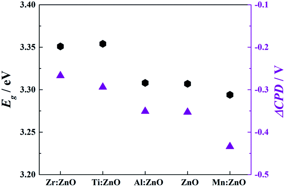
Band gap values and ΔCPD are mainly linked proportionally as it can be seen in a summary of both material parameters presented in Fig. 10. In the case of n-type dopants (such as the materials discussed here) it can be stated that the lower the band gap is, the lower the ΔCPD becomes. The ΔCPD of W:ZnO was not determined as the photon energy used for the study was in the sub-band gap range for this material. All other films (n-doped or pristine ZnO) have a significant potential drop and therefore generation of a photovoltage caused by illumination. As Mn:ZnO has the lowest band gap, it shows the highest ΔCPD of all analysed samples, whereas for Zr:ZnO it is vice-versa. This proves that SKP is a very relevant tool for fast and reliable characterization of photoactive materials.
 | ||
| Fig. 10 Left axis: values of optical bandgaps obtained from Tauc plots; right axis: SPV of the respective materials. | ||
The calculated charge carrier densities according to eqn (2) derived from the SKP measurements in the illuminated and not illuminated states are presented in Fig. 11. As it was mentioned before, since W doped ZnO needs higher photon energies to receive a response at the SKP, only the charge carrier density in the dark state is presented for this material. Average CPD values before and after the first illumination period were taken for the calculations in order to exclude relaxation effects attributed to slow recombination processes. The result obtained here for the dark state of ZnO is lower than those found in the literature for sputtered ZnO (e.g. ∼1017 cm−3).22 It is known that the charge carrier density depends strongly on the process parameters of the preparation (e.g. presence of oxygen, pressure during deposition, etc.). As the sputtered layer consists of small grains with a large density of grain boundaries, the charge carrier density is rather low. The electron mobility through the grain boundaries is hindered due to the local potential barriers formed by adsorbed oxygen.40 Previous studies have demonstrated that grain boundary scattering due to adsorbed oxygen molecules (at the surface but also at grain boundaries) directly affects the charge carriers.41 An additional theory states that in ZnO at low carrier concentrations, the dominant scattering mechanism is defined by the grain boundary potentials that reduce the electron mobility and, therefore, the electrical conductivity of the material. Above a critical carrier concentration, these grain boundary potentials collapse and the material in principle assumes the properties of a single crystal.42 In the current work, the carrier concentration is increased during the illumination cycles, which may explain the observed enhanced carrier concentration. When illuminated, a large potential drop occurs and the charge carrier concentration increases drastically up to ∼1021 cm−3. All of these facts together with the SEM images explain the high resistivity and low charge carrier concentration in the dark state.
 | ||
| Fig. 11 Charge carrier density for various doped ZnO thin films in the illuminated/not illuminated state. | ||
4. Conclusions
Various doped ZnO materials deposited on ITO-coated substrates were compared amongst each other and to pristine ZnO regarding their morphological, structural and optoelectronic properties. W:ZnO showed an outstanding position as the fabricated layer is amorphous. Its Tauc plot analysis revealed an optical bandgap of 4.35 eV, which is significantly higher than the Eg of pristine ZnO (3.31 eV). The other doped ZnO films exhibit similar bandgaps to pristine ZnO. W:ZnO may be a promising candidate for research in thin film transistors. It may also be applied as a highly insulating material due to its low charge carrier density and tendency of amorphisation. Its blue shift, which was shown by UV-VIS measurement, indicated W:ZnO to be a promising candidate as an inhibitor of photocatalytic reactions.
Mn:ZnO indeed may be a suitable material for TCO and photocatalytic research due to its high transparency in the visible range, low bandgap and large photovoltage. An additional valuable feature is the fact that it leads to a red shift in the band gap, which makes it interesting for conducting further studies in the field of photocatalysis.
In addition, a charge carrier density calculation has been accomplished in this study. The results obtained here show that the materials are highly insulating in the dark state, whereas they are rather conductive in the illuminated state, which was indicated by the photoresponsivity affecting the Volta potential. The highly insulating character of all samples may be due to the sputtering process, as this caused a large density of grains and grain boundaries. Scattering of charge carriers at the grain boundaries occurs and by UV-illumination these potential barriers can be easily overcome resulting in a higher electrical conductivity. The enhanced, fast responding and almost fully reversible surface photovoltage of the tested materials may be a helpful feature for research into TCO, photovoltaics and photodiodes and even for water splitting technologies due to possible photocatalytic activity.
Conflicts of interest
There are no conflicts to declare.Acknowledgements
Sincere thanks are given to Dr Petr Rathner and Michal Kamenicky, MSc from the Institute of Organic Chemistry at JKU Linz for assistance with the UV-VIS spectroscopy measurements. The financial support by the Austrian Federal Ministry for Digital and Economic Affairs and the National Foundation for Research, Technology and Development in the frame of the Christian Doppler Laboratory for Combinatorial Oxide Chemistry (COMBOX) is gratefully acknowledged. Open Access publishing was supported by Johannes Kepler Open Access Publishing Fund.References
- L. Wang, D. B. Li, K. Li, C. Chen, H. X. Deng, L. Gao, Y. Zhao, F. Jiang, L. Li, F. Huang, Y. He, H. Song, G. Niu and J. Tang, Nat. Energy, 2017, 2, 17046 CrossRef CAS.
- S. Guha, Nat. Energy, 2017, 2, 17057 CrossRef.
- J. Kegel, I. M. Povey and M. E. Pemble, Nano energy, 2018, 54, 409 CrossRef CAS.
- M. A. Desai, A. N. Vyas, G. D. Saratale and S. D. Sartale, Int. J. Hydrogen Energy, 2019, 44, 2091 CrossRef CAS.
- K. Gupta, S. Brahma, J. Dutta, B. Rao and C. P. Liu, Nano energy, 2019, 55, 1 CrossRef CAS.
- N. Tripathy and D. H. Kim, Nano Convergence, 2018, 5, 27 CrossRef PubMed.
- N. Nasiri, D. Jin and A. Tricoli, Adv. Opt. Mater., 2019, 7, 1800580 CrossRef.
- D. Mora-Fonz and A. L. Shluger, Phys. Rev. B, 2019, 99, 014202 CrossRef CAS.
- S. Yue, J. Lu, R. Lu, S. Li, X. Li, J. Zhang, L. Chen and Z. Ye, Appl. Phys. Lett., 2018, 113, 013504 CrossRef.
- D. B. Ruan, P. T. Liu, Y. C. Chiu, P. Y. Kuo, M. C. Yu, K. J. Gan, T. C. Chien and S. M. Sze, RSC Adv., 2018, 8, 6925 RSC.
- S. Huber, C. C. Mardare, C. Kleber and A. W. Hassel, Phys. Status Solidi A, 2019, 216, 1800942 CrossRef.
- F. Viñes, A. Iglesias-Juez, M. Fernández-García and F. Illas, J. Phys. Chem. C, 2018, 122, 19082 CrossRef.
- H. Zhang, H. Liu, C. Lei, C. Yuan and A. Zhou, Vacuum, 2010, 85, 184 CrossRef CAS.
- C. Zhang, X.-l. Chen, X.-h. Geng, C.-s. Tian, Q. Huang, Y. Zhao and X.-d. Zhang, Appl. Surf. Sci., 2013, 274, 371 CrossRef CAS.
- N. M. S. Jahed, M. Mahmoudysepehr and S. Sivoththaman, Mater. Res. Express, 2016, 3, 116402 CrossRef.
- Y. Wang, J. Cheng, S. Yu, E. J. Alcocer, M. Shahid, Z. Wang and W. Pan, Sci. Rep., 2016, 6, 32711 CrossRef CAS.
- J. Li and X. Bi, J. Mater. Chem. C, 2018, 6, 10350 RSC.
- N. E. Sung, K. S. Lee and I. J. Lee, Thin Solid Films, 2018, 651, 42 CrossRef CAS.
- J.-C. Lin, M.-C. Huang, T. Wang, J.-N. Wu, Y.-T. Tseng and K.-C. Peng, Mater. Express, 2015, 5, 153 CrossRef CAS.
- R. Cui, K. Shen, M. Xu, D. Xiang and Q. Xu, Mater. Sci. Semicond. Process., 2016, 43, 155 CrossRef CAS.
- K. Yim, J. Lee, D. Lee, M. Lee, E. Cho, H. S. Lee, H.-H. Nahm and S. Han, Sci. Rep., 2017, 7, 40907 CrossRef CAS.
- C. Maragliano, S. Lilliu, M. S. Dahlem, M. Chiesa, T. Souier and M. Stefancich, Sci. Rep., 2014, 4, 4203 CrossRef CAS.
- A. Nazarov, E. Diler, D. Persson and D. Thierry, J. Electroanal. Chem., 2015, 737, 129 CrossRef CAS.
- D. Cavalcoli, B. Fraboni and A. Cavallini, Semicond. Semimetals, 2015, 91, 251 Search PubMed.
- L. Kronik and Y. Shapira, Surf. Sci. Rep., 1999, 37, 1 CrossRef CAS.
- K. Ellmer, A. Klein and B. Rech, Transparent Conductive Zinc Oxide: Basics and Applications in Thin Film Solar Cells: Basics and Applications in Thin Film Solar Cells, Springer, Berlin Heidelberg, 2008 Search PubMed.
- Q. Shao, C. Wang, J. A. Zapien, C. W. Leung and A. Ruotolo, J. Appl. Phys., 2015, 117, 17B908 CrossRef.
- M. Gabás, P. Torelli, N. T. Barrett, M. Sacchi and J. R. Ramos Barrado, APL Mater., 2014, 2, 12112 CrossRef.
- A. Nakrela, N. Benramdane, A. Bouzidi, Z. Kebbab, M. Medles and C. Mathieu, Results Phys., 2016, 6, 133 CrossRef.
- A. Stadler, Photonik der Solarzellen: Innovative Messverfahren für moderne Solarzellen: Innovative Messverfahren für moderne Solarzellen, Springer Fachmedien Wiesbaden, Wiesbaden, 2015 Search PubMed.
- E. Burstein, Phys. Rev., 1954, 93, 632 CrossRef CAS.
- S. Herodotou, R. E. Treharne, K. Durose, G. J. Tatlock and R. J. Potter, Materials, 2015, 8, 7230 CrossRef CAS.
- S. D. Shinde, S. K. Date, A. V. Deshmukh, A. Das, P. Misra, L. M. Kukreja and K. P. Adhi, RSC Adv., 2015, 5, 24178 RSC.
- J. S. Kim, B. Lägel, E. Moons, N. Johansson, I. D. Baikie, W. R. Salaneck, R. H. Friend and F. Cacialli, Synth. Met., 2000, 111–112, 311 CrossRef CAS.
- S. D. Nehate, A. Prakash, P. D. Mani and K. B. Sundaram, ECS J. Solid State Sci. Technol., 2018, 7, P87–P90 CrossRef CAS.
- J. R. Harwell, T. K. Baikie, I. D. Baikie, J. L. Payne, C. Ni, J. T. S. Irvine, G. A. Turnbull and I. D. W. Samuel, Phys. Chem. Chem. Phys., 2016, 18, 19738 RSC.
- Q. Zhao, D. Wang, L. Peng, Y. Lin, M. Yang and T. Xie, Chem. Phys. Lett., 2007, 434, 96 CrossRef CAS.
- M. Ali Deeb, J. Ledig, J. Wei, X. Wang, H. H. Wehmann and A. Waag, J. Appl. Phys., 2017, 122, 85307 CrossRef.
- R. Chen, F. Fan, T. Dittrich and C. Li, Chem. Soc. Rev., 2018, 47, 8238 RSC.
- V. H. Nguyen, U. Gottlieb, A. Valla, D. Muñoz, D. Bellet and D. Muñoz-Rojas, Mater. Horiz., 2018, 5, 715 RSC.
- V. H. Nguyen, D. Bellet, B. Masenelli and D. Muñoz-Rojas, ACS Appl. Nano Mater., 2018, 1, 6922 CrossRef CAS.
- V. Srikant and D. R. Clarke, J. Mater. Res., 1997, 12, 1425 CrossRef CAS.
| This journal is © The Royal Society of Chemistry 2019 |