
 Open Access Article
 This Open Access Article is licensed under a
 Creative Commons Attribution 3.0 Unported Licence
A ternary SnS1.26Se0.76 alloy for flexible broadband photodetectors†
Lena Du‡
 ab,
Cong Wang‡abc,
Jingzhi Fangd,
Bin Weie,
Wenqi Xiongf,
Xiaoting Wangd,
Lijun Maab,
Xiaofeng Wangab,
Zhongming Weid,
Congxin Xiaf,
Jingbo Li*d,
Zhongchang Wang*e,
Xinzheng Zhang*c and
Qian Liu*abcd
ab,
Cong Wang‡abc,
Jingzhi Fangd,
Bin Weie,
Wenqi Xiongf,
Xiaoting Wangd,
Lijun Maab,
Xiaofeng Wangab,
Zhongming Weid,
Congxin Xiaf,
Jingbo Li*d,
Zhongchang Wang*e,
Xinzheng Zhang*c and
Qian Liu*abcd
aCAS Key Laboratory of Nanosystem and Hierarchical Fabrication, CAS Center for Excellence in Nanoscience, National Center for Nanoscience and Technology, Beijing 100190, P. R. China
bUniversity of Chinese Academy of Sciences, Beijing 100049, P. R. China. E-mail: liuq@nanoctr.cn
cThe MOE Key Laboratory of Weak-Light Nonlinear Photonics, TEDA Institute of Applied Physics, Nankai University, Tianjin 300457, P. R. China. E-mail: zxz@nankai.edu.cn
dState Key Laboratory of Superlattices and Microstructures, Institute of Semiconductors, Chinese Academy of Sciences, Beijing 100083, P. R. China. E-mail: jbli@semi.ac.cn
eDepartment of Quantum and Energy Materials, International Iberian Nanotechnology Laboratory (INL), Avenida Mestre José; Veiga s/n, Braga 4715-330, Portugal. E-mail: zhongchang.wang@inl.int
fDepartment of Physics, Henan Normal University, Xinxiang 453007, P. R. China
First published on 7th May 2019
Abstract
Layered two-dimensional (2D) materials often display unique functionalities for flexible 2D optoelectronic device applications involving natural flexibility and tunable bandgap by bandgap engineering. Composition manipulation by alloying of these 2D materials represents an effective way in fulfilling bandgap engineering, which is particularly true for SnS2xSe2(1−x) alloys showing a continuous bandgap modulation from 2.1 eV for SnS2 to 1.0 eV for SnSe2. Here, we report that a ternary SnS1.26Se0.76 alloy nanosheet can serve as an efficient flexible photodetector, possessing excellent mechanical durability, reproducibility, and high photosensitivity. The photodetectors show a broad spectrum detection ranging from visible to near infrared (NIR) light. These findings demonstrate that the ternary SnS1.26Se0.76 alloy can act as a promising 2D material for flexible and wearable optoelectronic devices.
1 Introduction
Flexible optoelectronic devices that can be bent, stretched, twisted and folded have triggered wide interest due to their greater superiorities in flexibility, lightweight and transparency,1–3 and thus have potential applications in flexible solar cells,4 video imaging,5 optical fiber communication.6 muscle-like transducers,7 machine vision,8 and so forth. Layered 2D materials are naturally suitable for various thin-film (opto)electronic devices due to their ultrathin thickness and flexibility.9,10 Although graphene has excellent mechanical11 and (opto)electronic12 properties and can offer a series of new possibilities at reduced dimensionality, it is limited to application in photoelectronic devices due to its gapless nature.13 As an alternative, several 2D materials with sizable bandgaps and superior (opto)electronic performances14–16 have been considered as potential candidates for next-generation ultrathin and flexible photoelectronics.17 For example, significant attention has been devoted to monolayer MoS2, which exhibits a photoresponsivity as high as 5.75 × 10³ A W−1 at a bias voltage of 5 V.18 The carrier mobility of MoS2 at extremely low temperature can be as high as 34![[thin space (1/6-em)]](https://www.rsc.org/images/entities/char_2009.gif) 000 cm2 V−1 s−1,19 and could be increased by strain engineering.20 In addition to the choice of materials, bandgap engineering21,22 enables to the modulation of electronic structure of 2D materials (e.g. indirect-to-direct transition), thus manipulating their optical and electronic properties. To date, alloying 2D materials has been demonstrated to be an effective way in fulfilling bandgap engineering for many optoelectronic applications.23,24
000 cm2 V−1 s−1,19 and could be increased by strain engineering.20 In addition to the choice of materials, bandgap engineering21,22 enables to the modulation of electronic structure of 2D materials (e.g. indirect-to-direct transition), thus manipulating their optical and electronic properties. To date, alloying 2D materials has been demonstrated to be an effective way in fulfilling bandgap engineering for many optoelectronic applications.23,24
As environmental-friendly, reserve-abundant and low-cost materials, layered tin dichalcogenides (SnS2, SnSe2) are desirable for sustainable development of flexible optoelectronic devices. Alloying of SnS2 and SnSe2 is often effective for bandgap engineering, in which a continuously tunable bandgap of SnS2xSe2(1−x) (0 < x < 1) from 2.1 eV (SnS2) to 1.0 eV (SnSe2) could be achieved.25 The layered SnS2 has a rapid photoresponsive feature with response time as short as 5 μs,26 and 1T atomic layered SnSe2 with a very close bandgap to silicon (1.1 eV) displays a good responsivity of 0.5 A W−1 and a fast response time of 2.2 ± 0.3 ms.27 Previous reports indicated that physical properties of a ternary compound SnS2xSe2(1−x) can be tunable by varying the atomic composition x, giving rise to remarkable (opto)electronic properties that may not appear in either of its binary compounds.28,29 As a member of SnS2xSe2(1−x) alloy, few layered SnS1.26Se0.76 (x ∼ 0.6) with a hexagonal CdI2-type structure in space group P![[3 with combining macron]](https://www.rsc.org/images/entities/char_0033_0304.gif) m1 is easily obtained by mechanical exfoliation from a crystal due to weak van der Waals force among layers. This low-dimensional semiconductor nanosheets with applicable bandgap represents a typical candidate for flexible optoelectronic devices due to its excellent optoelectronic properties possibly for broad spectra detection. However, the reports so far on the SnS1.26Se0.76 nanosheet-based flexible optoelectronic devices are very scarce, especially in the aspects of its mechanical durability, reproducibility, and high photo-sensitivity. In this work, we investigate flexible photodetectors based on ternary SnS1.26Se0.76 nanosheets, and demonstrate that the photodetectors exhibit a high photoresponsivity of ∼262 A W−1, a high detectivity of 1.98 × 10¹¹ jones and a fast response time of ∼10 ms to 532 nm light. Interestingly, the devices display a broad spectra response ranging from visible to NIR light and an ultrasensitive, reversible, and mechanical durable photoresponse even after being bent for 100 times. The findings suggest that SnS1.26Se0.76 can act as a promising 2D material for flexible and wearable optoelectronic devices.
m1 is easily obtained by mechanical exfoliation from a crystal due to weak van der Waals force among layers. This low-dimensional semiconductor nanosheets with applicable bandgap represents a typical candidate for flexible optoelectronic devices due to its excellent optoelectronic properties possibly for broad spectra detection. However, the reports so far on the SnS1.26Se0.76 nanosheet-based flexible optoelectronic devices are very scarce, especially in the aspects of its mechanical durability, reproducibility, and high photo-sensitivity. In this work, we investigate flexible photodetectors based on ternary SnS1.26Se0.76 nanosheets, and demonstrate that the photodetectors exhibit a high photoresponsivity of ∼262 A W−1, a high detectivity of 1.98 × 10¹¹ jones and a fast response time of ∼10 ms to 532 nm light. Interestingly, the devices display a broad spectra response ranging from visible to NIR light and an ultrasensitive, reversible, and mechanical durable photoresponse even after being bent for 100 times. The findings suggest that SnS1.26Se0.76 can act as a promising 2D material for flexible and wearable optoelectronic devices.
2 Experimental
2.1 Growth of SnS1.26Se0.76 crystal
SnS1.26Se0.76 crystal was synthesized by reacting the pure elements in quartz ampoules via chemical vapor transport using iodine as transport agent.30,31 Specific stoichiometric uniform mixtures of Sn powder (Alfa Aesar, 99.98%), sublimed S powder (Alfa Aesar, 99.5%), and Se powder (Alfa Aesar, 99+%) were mixed in air and put into quartz tubes, and then sealed into the furnace to sinter for getting SnS1.26Se0.76 polycrystal. Subsequently, the SnS1.26Se0.76 polycrystal was mixed with iodine (density: 5 mg cm−3), followed by seal in the silica tubes and heating for 10–20 days in a horizontal two-zone furnace. The as-grown SnS1.26Se0.76 single crystal was transported from the hot to cold zone. Finally, the SnS1.26Se0.76 crystal was obtained by natural cooling to room temperature.2.2 Structural characterization of as-synthesized SnS1.26Se0.76 crystal
The crystallographic structures of bulk SnS1.26Se0.76 were examined by X-ray diffraction (XRD, D/MAX-TTRIII (CBO)) technique. Morphologies were characterized by field emission scanning electron microscopy (FESEM, S4800,Tokyo, Japan). Specimens for transmission electron microscopy (TEM) and scanning transmission electron microscopy (STEM) observations were prepared by transferring SnS1.26Se0.76 nanosheets to the micro TEM grid. The TEM, high resolution TEM (HRTEM), selected area electron diffraction (SAED) and high-angle annular dark-field (HAADF) and bright-field (BF) STEM images were acquired by double aberration-corrected scanning transmission electron microscope (FEI G3 Cubed Themis 60–300 kV Monochromated X-FEG S/TEM). The elemental analysis were carried out by energy dispersive X-ray spectroscopy on the STEM (EDS, Super-X EDX System: four windowless Silicon Drift Detector).2.3 Optical spectroscopy measurements of SnS1.26Se0.76 nanoplates
SnS1.26Se0.76 nanosheets with different thickness were mechanically exfoliated from bulk SnS1.26Se0.76 crystals onto a SiO2/Si substrate. Morphology and thickness of the SnS1.26Se0.76 nanosheets were obtained by a laser scanning confocal microscope (LSCM, Olympus, LEXT-OLS4000) and an atomic force microscope (AFM, Multimode 8, Bruker). The Raman mapping and spectrum were taken using a spectrometer with an excitation wavelength of 514 nm (Renishaw inVia), aimed to characterize the composition-dependent vibration modes of the synthesized SnS1.26Se0.76 alloy crystals. Micro-photoluminescence (PL) spectrum was measured with the same instrument (Renishaw inVia). Theoretical calculations of the optical bandgap and electronic band structure for the bilayer and multilayer SnS1.26Se0.76 nanosheets were carried out based upon density functional theory (DFT).2.4 Fabrication and measurements of photodetector
For the device fabrication, SnS1.26Se0.76 nanosheets were obtained by mechanically exfoliating of bulk SnS1.26Se0.76 crystals onto a flexible PET substrate. TEM copper grid as a shadow mask with a typical gap of 15 μm was mounted on surface of flexible PET substrate covered by SnS1.26Se0.76 nanosheets. 10 nm Cr and 60 nm Au were subsequently evaporated as the electrodes of two-terminal photodetector, and the devices were prepared after removing the copper grid. All the electrical measurements were performed with a semiconductor test system (Agilent-B2902) at room temperature in the ambient. The 450, 532, 638 and 808 nm lasers were employed to perform photoresponse experiments.3 Results and discussion
3.1 Structural characterization of as-synthesized SnS1.26Se0.76 crystal
Bulk SnS1.26Se0.76 single crystals were synthesized by the chemical vapor transport (CVT) method with iodine as a transport agent (see Experimental). Fig. 1(a) presents the atomic structure of SnS1.26Se0.76 viewed from side and top, showing that it has a hexagonal CdI2-type structure with periodic S(Se)–Sn–S(Se) stacking along the c-axis and connecting with each layer through van der Waals forces. X-ray diffraction (XRD) of the synthesized SnS1.26Se0.76 single crystals (Fig. 1(b)) reveals five sharp peaks which correspond to (001), (002), (003), (004), and (005) peak derived from c-axis of the bulk, consolidating its single crystalline nature. The inset of Fig. 1(b) shows a FESEM image of SnS1.26Se0.76 single crystal exhibiting its layered structure. Further EDS analysis (Fig. 1(c)) reveals that the Sn/S/Se atomic ratio in the sample is roughly estimated to be 1:1.26:0.76, matching well with the nominal formula of SnS2xSe2(1−x) (x ∼ 0.6). Fig. 1(d)–(g) shows a typical TEM image of a SnS1.26Se0.76 few-layer flake and the corresponding EDS element mapping for Sn, S and Se. The EDS mappings confirm a highly uniform distribution of Sn, S and Se elements.
 | ||
| Fig. 1 Structural characterization of as-synthesized SnS1.26Se0.76 crystal. (a) Atomic model of SnS1.26Se0.76 from a side and top view (along the [001] direction). (b) Single-crystal XRD spectrum. Inset: SEM image shows the layered structure of SnS1.26Se0.76. (c) Energy-dispersive spectroscopy (EDS) result. (d) Typical TEM image of a SnS1.26Se0.76 flake and corresponding EDS element mapping image for (e) Sn (f) S and (g) Se. (h) High-resolution TEM (HRTEM) image of SnS1.26Se0.76 viewed along [001] direction. (i) The corresponding selected area electron diffraction (SAED) pattern. (j and k) Atomic scale HAADF and BF STEM image of SnS1.26Se0.76 along [001] direction. | ||
Fig. 1(h) shows HRTEM image of the SnS1.26Se0.76 sample, revealing a hexagonal structured lattice with an interplanar distance of 0.34 nm, consistent with that of the (100) plane of SnS1.26Se0.76. The corresponding SAED pattern shown in Fig. 1(i) displays the lattice arrangement, indicating that the SnS1.26Se0.76 sample is stacked along [001] direction with good crystallinity. To further extract atomic information, we show in Fig. 1(j) and (k) atomic-resolution HAADF and BF STEM images of the SnS1.26Se0.76 flake viewed from the [001] axis. Since intensity of an atomic column in a HAADF STEM imaging mode is proportional to Z1.7 (Z is atomic number),32–34 the brightest spots (corresponding to the highest intensity line profile in Fig. S1(c)†) represent the Sn atomic columns (Z = 50), while the medium-brightness and lowest-brightness spots (corresponding to the medium–high and lowest intensity line profile in Fig. S1(c),† respectively) represent the Se-rich (Z = 34) and S-rich (Z = 16) atomic columns, respectively, as also sketched in Fig. S1(d).† Interestingly, the Se and S atoms are partially ordered and periodically distributed in the SnS1.26Se0.76 single crystal. The obtained atomic-resolution HAADF and BF STEM images (Fig. 1(k) and (j)) agree well with the atomic model (Fig. 1(a)), showing a symmetrical hexagonal lattice fringe due to the equivalent locations of Se and S in the atomic structure of SnS1.26Se0.76.
3.2 Optical properties of SnS1.26Se0.76 nanoplates
The few-layer SnS1.26Se0.76 was mechanically exfoliated from SnS1.26Se0.76 crystals onto a SiO2/Si substrate. Fig. 2(a) shows optical images of the 2D layered SnS1.26Se0.76 with different thicknesses that can be reflected by different colors. Further AFM topography (Fig. 2(b)) reveals that the area of the palest blue color in the orange square in Fig. 2(a) has a thickness of 2.36 nm (i.e. 2–3 layer). To characterize the composition dependent vibration modes of the SnS1.26Se0.76 crystal, we present in Fig. 2(c) Raman mapping image for the intensity of A1g(Sn–Se) vibration peak (200–205 cm−1). The intensity of bilayer SnS1.26Se0.76 sample is much weaker than that of few-layer one, as is also reflected in the thickness-dependent Raman spectrum (Fig. 2(d)). All the samples have characteristic peaks at about 204 and 304 cm−1, which are assigned to the A1g(Sn–Se) and A1g(Sn–S) vibration modes,35,36 while the weak peaks located at 136 cm−1 is assigned to in-plane mode Eg(Sn–Se). The Raman mode of Eg(Sn–S) is not observed possibly resulting from the weak electron–phonon interaction in thin layer samples. For the flakes with different thicknesses, the positions of these observed peaks almost remain unchanged but their intensities increase with the thickness of SnS1.26Se0.76 nanosheets. The Raman peak positions are almost the same for the samples with thicknesses ranging from 2.36 to 12.13 nm, indicating that the layer thickness has minor effect on Raman behavior.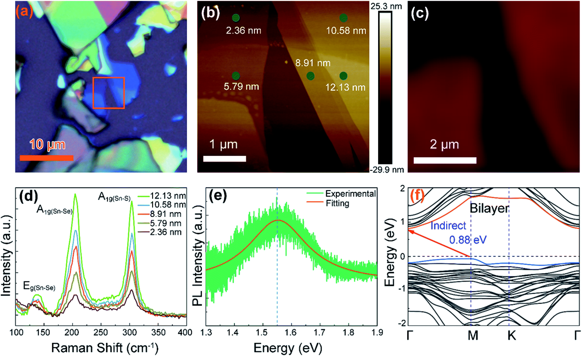 | ||
| Fig. 2 Optical properties of SnS1.26Se0.76 nanoplates deposited on SiO2/Si substrate. (a) Optical and (b) AFM images with different color showing different thickness. The thickness of 2.36 nm measured by AFM is about 2–3 layers. (c) Raman (200–205 cm−1) mapping image about the intensity of A1g(Sn–Se) vibration mode measured in the same SnS1.26Se0.76 sample. (d) Raman spectrum dependent on thickness. (e) Photoluminescence spectrum and (f) calculated electronic band structure of bilayer SnS1.26Se0.76 indicating bilayer SnS1.26Se0.76 is an indirect bandgap semiconductor. The calculation also demonstrates bulk SnS1.26Se0.76 is indirect bandgap semiconductor. | ||
Fig. 1(e) shows PL spectrum, where the intense peak position is located at about 1.55 eV, indicating that the optical bandgap is 1.55 eV. The intensity of PL is weaker for thicker sample due to the indirect bandgap nature of SnS1.26Se0.76, which can also be proven by calculated electronic band structure of bilayer and bulk SnS1.26Se0.76 (Fig. 2(f) and S2†). From Fig. 2(f), the bilayer SnS1.26Se0.76 is calculated to be an indirect band gap semiconductor with conduction band minimum (CBM) located at Γ point and valence band maximum (VBM) at M point. This differs from the SnS1.26Se0.76 bulk case showing an indirect band gap CBM at Γ point and VBM at a general point along M–Γ line (Fig. S2†). The bandgaps for the bilayer and bulk SnS1.26Se0.76 are estimated as 0.88 eV and 0.94 eV, respectively, which are smaller than the experimental data due to the well-known underestimation of bandgap in the hybrid functional theory (HSE06).37 The narrower bandgap for the bilayer with respect to its bulk implies a broad spectra detection from visible to NIR light for optoelectronic device applications.
3.3 Photoresponse of flexible optoelectronic devices based on SnS1.26Se0.76 nanosheets
To probe the broad spectrum optoelectronic characteristic of SnS1.26Se0.76, we fabricate flexible photodetectors based on SnS1.26Se0.76 nanopsheets on PET substrate by traditional device fabrication techniques and measure the photoresponse from visible to NIR light. Fig. 3(a) sketches the structure of a SnS1.26Se0.76 nanosheets-based two-terminal flexible photodetector (inset signifies the optical image of electrodes array). Fig. 3(b–e) exhibit high photoresponse to 532 nm light with various illumination. Fig. 3(b) shows the typical I–V curves of a device (inset of Fig. 3(b)) in the dark and under different irradiances at 532 nm. The observed linear plots of I–V indicate an ohmic contact between the SnS1.26Se0.76 film and Au/Cr electrodes. Upon decreasing the light irradiance, the photocurrent decreases, while the photoresponsivity increases (Fig. 3(c)). Here, photocurrent (Iph) is defined as the differences between Iilluminated and Idark (Iph = Iilluminated − Idark) and photoresponsivity (Rλ) is defined as the photocurrent generated per unit power of incident light on the effective area (S) (Rλ = Iph/PS). In addition, the detectivity (D*) reflects the photodetector's sensitivity, and can be calculated by D* = RλS1/2/(2eIdark)1/2, where e is the electronic charge. At a bias voltage of 2 V and a light irradiance of 3.4 mW cm−2, the device shows a photoresponsivity of 262 A W−1 and a detectivity of 1.98 × 10¹¹ jones under the illumination of 532 nm laser. The efficient irradiation area S is 120 μm2. The corresponding light intensity dependence of the photocurrent can be expressed by a power law function of Iph ∼ Pα, which indicates increased photons generate more electrons. A power dependence of Iph ∼ P0.53 is estimated for our photodetector by fitting the experimental data, and the deviation from the ideal slope may be attributed to the long-channel in the SnS1.26Se0.76 photodetector.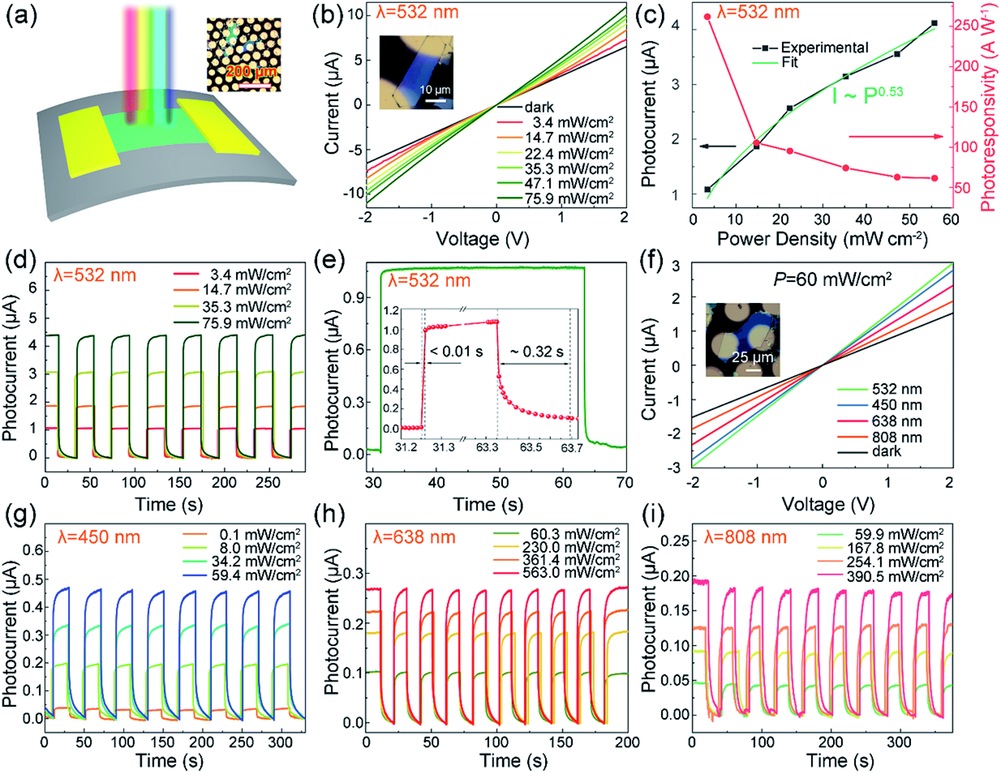 | ||
| Fig. 3 Photoresponse of flexible optoelectronic devices based on SnS1.26Se0.76 nanoplates fabricated on PET substrate. (a) Schematic illustration of the structure of a SnS1.26Se0.76 nanosheets-based two-terminal optoelectronic device; inset is the optical image of electrodes array. (b) I–V curves in the dark and under different irradiances with laser wavelength of 532 nm; inset is the optical image of the device and thickness is ∼60 nm. (c) Plots of the photocurrent and photoresponsivity against irradiance at 2 V bias (532 nm light). (d) Time-dependent photoresponse of SnS1.26Se0.76 nanoplate device at various light intensity at 2 V bias (532 nm light). (e) A separated temporal photocurrent response and reset cycle; inset is an enlarged view of the temporal photocurrent response. (f) I–V curves in the dark and in the presence of 375, 473, and 632 nm laser of a single SnS1.26Se0.76 nanoplate photodetector at a fixed irradiance of 60 mW cm−2; inset is the optical image of the device. (g)–(i) are time-dependent photoresponse of SnS1.26Se0.76 nanoplate device under different irradiances with laser wavelength of 450 nm, 638 nm and 808 nm, respectively. The corresponding voltage bias is 2 V. | ||
To shed light on the photoresponse with the laser on and off, we measure time-dependent photoresponse of SnS1.26Se0.76 nanosheet-based devices at various light intensity at 2 V bias (532 nm light) as shown in Fig. 3(d). With the on/off switching of incident laser, a highly stable and reversible photo-switching behavior between two states is observed and the sharp rise and drop of current with light on and off confirm that the device is ultrasensitive to light. The response time (τon, defined as he time needed to reach 90% of the maximum photocurrent) and recovery time (τoff, defined as the time needed to drop to 10% of the maximum photocurrent) are estimated to be ∼0.01 s and ∼0.32 s, respectively, from an enlarged single circle in Fig. 3(e), which are superior to the values reported for most of layered materials.38,39 To evaluate the performance of our fabricated SnS1.26Se0.76 photodetectors, we list in Table 1 the outstanding figure-of-merit of some devices reported for other 2D tin dichalcogenides.26,27,40–42 As can be seen from Table 1, the response time in our work is very fast, but the decay time is longer than most of the previous report. The decay time of the device contains three procedures: the first stage is the recombination of excess carrier, followed by the empty of shallow and deep traps, respectively.43 According to the atom ratio measured by EDS, we can confirm that there are small amount of Sn vacancies appearing in SnS1.26Se0.76 crystal during the synthesis process. Therefore, the observed long decay time of the device was caused by the slow release of electrons trapped in the Sn vacancies-induced deep traps44,45 because the de-trap time of carriers from a deep trap can be prolonged by several orders of magnitude as compared to shallow traps, resulting in additional decay of the device.46,47 In addition, the SnS1.26Se0.76 shows pronounced photoresponse under a voltage bias of 2 V for 450, 532, 638, and 808 nm laser (Fig. 3(f)), and the devices show a high stability under different irradiances for different laser wavelengths (Fig. 3(d, g–i)). The SnS1.26Se0.76 photodetector exhibits the highest Rλ to 532 nm light (∼262 A W−1) and a relatively low Rλ to NIR light (∼120 mA W−1). The related performance parameters are listed in Table 2 and detailed experimental data are given in Fig. S4–S6.† As summarized in Tables 1 and 2, our photodetector shows a good photoresponse, indicating that the SnS1.26Se0.76 nanosheets can serve as an ideal 2D material as high-performance photodetectors. Further work we will focus on the study of increasing photocurrent by decreasing membrane thickness or fabricating heterojunction structure and improve experimental method to study the response to weaker light.48,49
| Materials | Synthesis method | Wavelength [nm] | Rλ [mA W−1] | Rise time [ms] | Decay time [ms] | D* [jones] | Ref. |
|---|---|---|---|---|---|---|---|
| a Flexible photodetector. | |||||||
| SnS2 | CVD | 365 | 2.6 × 10⁵ | 20 | 16 | 1010 | 40 |
| SnS2 | CVD | 457 | 8.8 | 5 × 10⁻³ | 7 × 10⁻³ | 109 | 26 |
| SnS2a | — | 405 | 4.7 × 10⁻⁴ | 820 | 620 | — | 41 |
| SnSe2 | CVD | 530 | 1.1 × 10⁶ | 14.5 | 8.1 | 1010 | 42 |
| SnSe2 | CVT | 633 | 500 | 2.1 | 3.2 | — | 27 |
| SnS1.26Se0.76a | CVT | 532 | 2.62 × 10⁵ | <10 | 320 | 1011 | This work |
| Wavelength [nm] | Rise time [s] | Recovery time [s] | Rλ [mA W−1] | |
|---|---|---|---|---|
| a These devices are measured under illumination of the 532 nm, 450 nm, 638 nm and 808 nm laser with a light intensity of 3.4 mW cm−2, 8.0 mW cm−2, 60.3 mW cm−2 and 59.9 mW cm−2, respectively. The corresponding voltage bias are all 2 V.b These PET devices are measured after bending 100 times with a bending radius of 5.5 mm. | ||||
| 532 | PET | <0.01 | 0.32 | 2.62 × 10⁵ |
| PETb | <0.01 | 0.32 | 2.50 × 10⁵ | |
| 450 | PET | 1 | 8 | 11.42 × 10³ |
| PETb | 1 | 8 | 10.01 × 10³ | |
| 638 | PET | 0.45 | 2.4 | 273 |
| PETb | 0.45 | 2.4 | 262 | |
| 808 | PET | 2 | 2.5 | 120 |
| PETb | 2 | 2.5 | 98 | |
3.4 Durability of SnS1.26Se0.76 flexible photodetector
Apart from the stability and sensitivity, mechanical flexibility is also an important parameter to evaluate for the flexible photodetector. In order to assess the durability of the SnS1.26Se0.76 flexible optoelectronic devices, the devices were bent repeatedly for 100 times with a bending radius of 5.5 mm, as shown in Fig. 4(a) and (b). Fig. 4(c) shows the I–V characteristics of the photodetector under a dark and 532 nm laser irradiance of 3.4 mW cm−2 and Fig. 4(d) under a dark and 808 nm laser irradiance of 59.9 mW cm−2 after bending for 100 times. The I–V plots differ slightly for both dark current and photocurrent compared with unbending case, which can be attributed to the destructive contact barrier between SnS1.26Se0.76 nanosheet and electrodes after plenty of continuous mechanical bending. Although the photocurrent has a slight decrease after bending, a sharp increase in photocurrent is observed once the devices is illuminated by either 532 nm laser or 808 nm laser, as shown in Fig. 4(e) and (f). Similar time trace of photoresponse is also observed under illumination with 450 nm and 638 nm laser, as shown in Fig. S7.† From the time-dependent photocurrent, we can see that when the laser switches from “OFF” to “ON” state, the current rapidly reaches a relatively large value and then slowly increases to a saturation value. The photocurrent decreases from ∼1.08 μA to ∼1.03 μA under 532 nm laser illumination of 3.4 mW cm−2 at a bias of 2 V, which leads to a minor decrease in photoresponsivity from 262 A W−1 to 250 A W−1. However, the response time and recovery time remain almost unchanged after sustaining 100 times of bending. The photoresponse parameters of τon, τoff and Rλ are summarized in Table 2 before and after bending 100 times with different illumination wavelength. These findings show that SnS1.26Se0.76 nanosheet-based photodetector maintains excellent mechanical durability, reproducibility, and high photo-sensitivity, demonstrating great potential for advanced flexible and wearable optoelectronic device applications.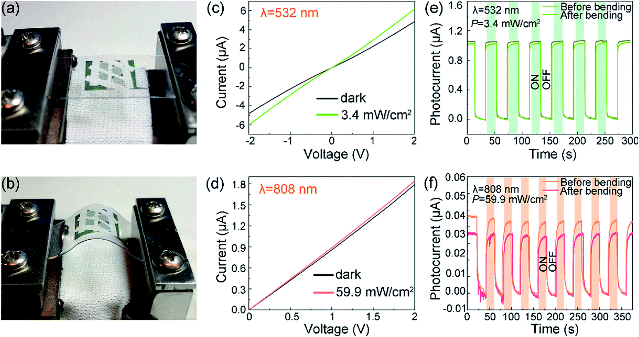 | ||
| Fig. 4 Durability measurements of SnS1.26Se0.76 flexible photodetector on PET substrate. (a) and (b) Photograph of instrument used for bending. (c) and (d) I–V curves under 532 nm laser irradiance of 3.4 mW cm−2 and 808 nm laser irradiance of 59.9 mW cm−2, respectively, after bending the device for 100 times. The black curves refer to dark current. (e) and (f) Time trace of photoresponse under illumination with 532 nm and 808 nm laser before and after bending the device for 100 times. The laser power intensity is set to 3.4 mW cm−2, and 59.9 mW cm−2, respectively. (2 V bias voltage and 5.5 mm bending radius). | ||
4 Conclusions
We perform a systematic study on flexible photodetectors based on high-quality single crystalline ternary SnS1.26Se0.76 nanosheets. The photodetectors exhibit a good broad spectra photoresponse in the region of visible (450 nm) to NIR (808 nm) light, high photoresponsivity of ∼262 A W−1, and fast response time of ∼10 ms to 532 nm light. Furthermore, such photodetector can maintain excellent mechanical durability, reproducibility, and high photo-sensitivity even after being bent for 100 times with a bending radius of 5.5 mm, showing great potential in the application of advanced flexible and wearable optoelectronic devices. The findings pay a new way in employing other layered alloy materials in flexible optoelectronic devices based on bandgap engineering.Author contributions
C. W. and Q. L. approached this idea. L. N. D. and C. W. contributed equally to this work. Q. L. and Cong Wang guided this research. L. N. D. and C. W. worked on device fabrication, performed the measurements and analyzed the data. L. N. D., C. W. and Q. L. wrote the manuscript. W. Q. X. performed electronic structure calculations. Z. C. W., Z. M. W., X. Z. Z. and J. B. L. made suggestions to improve this research. B. W. measured STEM and EDS. X. F. W. plotted the schematic illustration of SnS1.26Se0.76 flexible photodetector. We thank J. Z. F., X. T. W. and L. J. M. for their help in electrical measurements. All authors discussed experimental and theoretical results.Conflicts of interest
There are no conflicts to declare.Acknowledgements
This work is supported by the National Key Research Program of China (2016YFA0200403), Eu-FP7 Project (No. 247644), CAS Strategy Pilot Program (XDA 09020300). J. B. L., Z. M. W., C. X. X. and Z. C. W. thank the support from National Natural Science Foundation of China (Grant No. 61622406, 11674310, 61571415, 11674084, and 51728202). Z. X. Z. thanks the support from National Natural Science Foundation of China (91750204).Notes and references
- R. Cheng, Y. Wen, L. Yin, F. Wang, F. Wang, K. Liu, T. A. Shifa, J. Li, C. Jiang and Z. Wang, Adv. Mater., 2017, 29, 1703122 CrossRef.
- J. Song, J. Li, J. Xu and H. Zeng, Nano Lett., 2014, 14, 6298–6305 CrossRef CAS PubMed.
- S. Huang, Y. Liu, Y. Zhao, Z. Ren and C. F. Guo, Adv. Funct. Mater., 2018, 29, 1805924 CrossRef.
- Q. Luo, H. Ma, Q. Hou, Y. Li, J. Ren, X. Dai, Z. Yao, Y. Zhou, L. Xiang and H. Du, Adv. Funct. Mater., 2018, 28, 1706777 CrossRef.
- M. J. Gora, J. S. Sauk, R. W. Carruth, K. A. Gallagher, M. J. Suter, N. S. Nishioka, L. E. Kava, M. Rosenberg, B. E. Bouma and G. J. Tearney, Nat. Med., 2013, 19, 238 CrossRef CAS.
- D. Richardson, J. Fini and L. E. Nelson, Nat. Photonics, 2013, 7, 354 CrossRef CAS.
- D. J. Lipomi, M. Vosgueritchian, B. C. Tee, S. L. Hellstrom, J. A. Lee, C. H. Fox and Z. Bao, Nat. Nanotechnol., 2011, 6, 788 CrossRef CAS PubMed.
- Z. Liu, X. Li, F. Li, X. Wei and G. Zhang, Sensors, 2015, 15, 4643–4657 CrossRef.
- Q. H. Wang, K. Kalantar-Zadeh, A. Kis, J. N. Coleman and M. S. Strano, Nat. Nanotechnol., 2012, 7, 699 CrossRef CAS.
- F. Xia, H. Wang, D. Xiao, M. Dubey and A. Ramasubramaniam, Nat. Photonics, 2014, 8, 899 CrossRef CAS.
- C. Lee, X. Wei, J. W. Kysar and J. Hone, Science, 2008, 321, 385–388 CrossRef CAS.
- Q. Bao and K. P. Loh, ACS Nano, 2012, 6, 3677–3694 CrossRef CAS.
- D. B. Mitzi, L. L. Kosbar, C. E. Murray, M. Copel and A. Afzali, Nature, 2004, 428, 299 CrossRef CAS.
- Q. Wang, K. Xu, Z. Wang, F. Wang, Y. Huang, M. Safdar, X. Zhan, F. Wang, Z. Cheng and J. He, Nano Lett., 2015, 15, 1183–1189 CrossRef CAS.
- C. Wang, S. Yang, W. Xiong, C. Xia, H. Cai, B. Chen, X. Wang, X. Zhang, Z. Wei and S. Tongay, Phys. Chem. Chem. Phys., 2016, 18, 27750–27753 RSC.
- W. Wu, L. Wang, R. Yu, Y. Liu, S. H. Wei, J. Hone and Z. L. Wang, Adv. Mater., 2016, 28, 8463–8468 CrossRef CAS.
- M. Long, P. Wang, H. Fang and W. Hu, Adv. Funct. Mater., 2018, 1803807 CrossRef.
- D. H. Kang, M. S. Kim, J. Shim, J. Jeon, H. Y. Park, W. S. Jung, H. Y. Yu, C. H. Pang, S. Lee and J. H. Park, Adv. Funct. Mater., 2015, 25, 4219–4227 CrossRef CAS.
- X. Cui, G.-H. Lee, Y. D. Kim, G. Arefe, P. Y. Huang, C.-H. Lee, D. A. Chenet, X. Zhang, L. Wang and F. Ye, Nat. Nanotechnol., 2015, 10, 534 CrossRef CAS.
- T. Shen, A. V. Penumatcha and J. Appenzeller, ACS Nano, 2016, 10, 4712–4718 CrossRef CAS.
- G. G. Naumis, S. Barraza-Lopez, M. Oliva-Leyva and H. Terrones, Rep. Prog. Phys., 2017, 80, 096501 CrossRef.
- L. Du, C. Wang, W. Xiong, S. Zhang, C. Xia, Z. Wei, J. Li, S. Tongay, F. Yang, X. Zhang, X. Liu and Q. Liu, 2D Mater., 2019, 6, 025014 CrossRef.
- S. Tongay, D. S. Narang, J. Kang, W. Fan, C. Ko, A. V. Luce, K. X. Wang, J. Suh, K. Patel and V. Pathak, Appl. Phys. Lett., 2014, 104, 012101 CrossRef.
- J. Park, M. S. Kim, B. Park, S. H. Oh, S. Roy, J. Kim and W. Choi, ACS Nano, 2018, 12, 6301–6309 CrossRef CAS.
- Y. Wang, L. Huang, B. Li, J. Shang, C. Xia, C. Fan, H.-X. Deng, Z. Wei and J. Li, J. Mater. Chem. C, 2017, 5, 84–90 RSC.
- G. Su, V. G. Hadjiev, P. E. Loya, J. Zhang, S. Lei, S. Maharjan, P. Dong, P. M. Ajayan, J. Lou and H. Peng, Nano Lett., 2014, 15, 506–513 CrossRef.
- P. Yu, X. Yu, W. Lu, H. Lin, L. Sun, K. Du, F. Liu, W. Fu, Q. Zeng and Z. Shen, Adv. Funct. Mater., 2016, 26, 137–145 CrossRef CAS.
- P. Perumal, R. K. Ulaganathan, R. Sankar, Y. M. Liao, T. M. Sun, M. W. Chu, F. C. Chou, Y. T. Chen, M. H. Shih and Y. F. Chen, Adv. Funct. Mater., 2016, 26, 3630–3638 CrossRef CAS.
- T. Pan, D. De, J. Manongdo, A. Guloy, V. Hadjiev, Y. Lin and H. Peng, Appl. Phys. Lett., 2013, 103, 093108 CrossRef.
- F. Al-Alamy and A. Balchin, J. Cryst. Growth, 1977, 38, 221–232 CrossRef CAS.
- X. Wang, D. Chen, Z. Yang, X. Zhang, C. Wang, J. Chen, X. Zhang and M. Xue, Adv. Mater., 2016, 28, 8645–8650 CrossRef CAS.
- R. Esparza, A. Santoveña, A. Ruíz-Baltazar, A. Angeles-Pascual, D. Bahena, J. Maya-Cornejo, J. Ledesma-García and R. Pérez, Mater. Res., 2017, 20, 1193–1200 CrossRef.
- R. Erni, H. Heinrich and G. Kostorz, Ultramicroscopy, 2003, 94, 125–133 CrossRef CAS.
- S. Yang, C. Hu, M. Wu, W. Shen, S. Tongay, K. Wu, B. Wei, Z. Sun, C. Jiang and L. Huang, ACS Nano, 2018, 12, 8798–8807 CrossRef CAS.
- D. Mead and J. Irwin, Solid State Commun., 1976, 20, 885–887 CrossRef CAS.
- A. Smith, P. Meek and W. Liang, J. Phys. C: Solid State Phys., 1977, 10, 1321 CrossRef CAS.
- S. Park, B. Lee, S. H. Jeon and S. Han, Curr. Appl. Phys., 2011, 11, S337–S340 CrossRef.
- O. Lopez-Sanchez, D. Lembke, M. Kayci, A. Radenovic and A. Kis, Nat. Nanotechnol., 2013, 8, 497 CrossRef CAS.
- W. Zhang, M.-H. Chiu, C.-H. Chen, W. Chen, L.-J. Li and A. T. S. Wee, ACS Nano, 2014, 8, 8653–8661 CrossRef CAS.
- X. Zhou, Q. Zhang, L. Gan, H. Li and T. Zhai, Adv. Funct. Mater., 2016, 26, 4405–4413 CrossRef CAS.
- Y. Tao, X. Wu, W. Wang and J. Wang, J. Mater. Chem. C, 2015, 3, 1347–1353 RSC.
- X. Zhou, L. Gan, W. Tian, Q. Zhang, S. Jin, H. Li, Y. Bando, D. Golberg and T. Zhai, Adv. Mater., 2015, 27, 8035–8041 CrossRef CAS.
- J. Jiang, C. Ling, T. Xu, W. Wang, X. Niu, A. Zafar, Z. Yan, X. Wang, Y. You and L. Sun, Adv. Mater., 2018, 30, 1804332 CrossRef.
- Z. Zheng, J. Yao and G. Yang, ACS Appl. Mater. Interfaces, 2017, 9, 14920–14928 CrossRef CAS.
- L. Qian, Y. Sun, M. Wu, C. Li, D. Xie, L. Ding and G. Shi, Nanoscale, 2018, 10, 6837–6843 RSC.
- Y. Zhang, T. Liu, B. Meng, X. Li, G. Liang, X. Hu and Q. J. Wang, Nat. Commun., 2013, 4, 1811 CrossRef.
- Z. Hu, Z. Wu, C. Han, J. He, Z. Ni and W. Chen, Chem. Soc. Rev., 2018, 47, 3100–3128 RSC.
- Z. Zheng, J. Yao and G. Yang, J. Mater. Chem. C, 2016, 4, 8094–8103 RSC.
- Z. Zheng, J. Yao and G. Yang, ACS Appl. Mater. Interfaces, 2017, 9, 7288–7296 CrossRef CAS.
Footnotes |
| † Electronic supplementary information (ESI) available. See DOI: 10.1039/c9ra01734h |
| ‡ These authors contributed equally. |
| This journal is © The Royal Society of Chemistry 2019 |