
 Open Access Article
 This Open Access Article is licensed under a Creative Commons Attribution-Non Commercial 3.0 Unported Licence
Highly conductive carbon-based aqueous inks toward electroluminescent devices, printed capacitive sensors and flexible wearable electronics†
Yu Liaoab,
Rui Zhanga,
Hongxia Wanga,
Shuangli Yea,
Yihua Zhoua,
Taolin Maa,
Junqing Zhub,
Lisa D. Pfefferleb and
Jun Qian *a
*a
aSchool of Printing and Packaging, Wuhan University, Luojia Hill, Wuhan, 430072, China. E-mail: whuqianjun@163.com
bChemical & Environmental Engineering, School of Engineering & Applied Science, Yale University, 17 Hillhouse Avenue, New Haven, CT 06511, USA
First published on 15th May 2019
Abstract
Carbon-based conductive inks are one of the most important materials in the field of printing electronics. However, most carbon-based conductive inks with small electrical resistance are expensive, such as graphene. It limits the commercial use of carbon inks in the fields of flexible electronics and printed electronics. Here, we propose a low-cost and environmentally friendly formula based on dihydroxyphenyl-functionalized multi-walled carbon nanotubes (MWNT-f-OH)/carbon black/graphite as conductive fillers and waterborne acrylic resins as binders for preparing highly conductive carbon-based aqueous inks (HCCA-inks). Our study showed that when the mass fraction of carbon black, graphite and MWNT-f-OH was 3.0%, 10.2% and 4.1%, respectively, on a thickness of 40 μm, optimal conductivity (sheet resistance up to 29 Ω sq−1) was achieved, and the printed HCCA-inks on a paper could withstand extremely high folding cycles (>2000 cycles) while the resistance value of the flexible circuit only increased by 11%. The carbon-based aqueous inks showed high electrical conductivity and excellent mechanical stability, which makes it possible for them to be used as flexible wearable electronics, electroluminescent (EL) devices and printed capacitive sensors.
Introduction
Carbon materials as the additives in conductive inks have been widely applied in the field of printed electronics, especially the graphene and carbon nanotubes.1–5 Because of their exceptional chemical, mechanical, electrical, and optical properties, they can greatly improve the performance of conductive inks.6–10 Graphite is a laminar structure with several tens of microns long. Carbon black (CB) is a submicron-sized conductive sphere with larger specific surface area than graphite.11 Both of the carbon materials with different sizes are more conductive when combined together because the gaps between the conductive particles are smaller than any one of them when used in isolation.12 Small carbon blacks particles are more easily to disperse between the graphite gaps to form conductive bridges.13 Carbon nanotubes and graphene have been widely studied as conductive fillers for carbon conductive ink.14–16 However, they are restricted to high cost and difficult to disperse in aqueous solutions, so it is difficult to achieve a large-scale production in the field of printed electronics.3,17–20There are some reports on carbon conductive inks, as listed in Table s1.† Carlos C. B. Bufon et al.21 combined carbon black and cellulose acetate to achieve high-performance conductive tracks with sheet resistance (250 Ω sq−1, with a thickness of 9 μm). Chris Phillips et al.12 found that at a higher total carbon loading ink of 29.4% by mass, optimal conductivity (38.7–252.2 Ω sq−1, with a thickness of around 9.5 μm) was achieved at a graphite to CB ratio of 2.6 to 1. Ferdinand Hof et al.22 dispersed the prepared graphitic nanoparticles in water and obtained the conductive ink with sheet resistance as low as 220 Ω sq−1 on normalised thickness of 25 μm. Tso-Hsuan Chen et al.10 mixed carbon nanotubes (CNTs) with wax to formulate a solid composite for pen writing with the sheet resistance of 200 Ω sq−1 on a thickness of 90 μm. In fact, the resistance of these carbon conductive inks synthesized by the above methods are relatively large, and are not suitable for printed electronic products. Vasilios Georgakilas et al.2,23 dispersed Gr and MWNT-f-OH in water-soluble polymers resulting in record values of electrical conductivity (25 Ω sq−1, with a thickness of 2.86 μm). Siva Sankar Nemala et al.24 mixed 80 wt% Gr with 20 wt% polyamic acid made the ink with sheet resistance of 26 Ω sq−1 on a thickness of 15 μm. Obviously, these conductive inks conductivity are better, but they are very expensive.
In this work, we report a simple and efficient method based on MWNT-f-OH/CB/graphite as conductive fillers and waterborne acrylic resin as binder to prepare the HCCA-inks. It provides a new option for the commercial application of carbon ink in the field of printed electronics and flexible electronics. A series of comparative experiments were conducted to obtain a formula. Tenfold of the conductivity has been improved by adding the right amount of MWNT-f-OH which's an extended study of Chris Phillips et al.10,12,21,22 These inks could be applied to most printing techniques such as screen printing, flexography, or gravure printing. We also demonstrate the preparation of a large-sized (900 cm2) EL device with a power of 4.0 mW cm−2 using the conductive ink instead of silver paste as the back electrode, which's never reported in previous studies. Moreover, print-type capacitive sensing technology was combined to achieve the application of conductive ink printing sensors non-contact control light on and off.25–27 Moreover, the conductive ink was printed on a flexible substrate and its folding resistance was tested. After 2000 times of folding, the conductivity only decreased by 11%.
Experimental
Materials
All chemicals were of analytical grade. MWNT-f-OH were purchased from Shenzhen Inorganic Chemicals Co., Ltd, China. Graphite was acquired from Qingdao Yanhai Carbon Materials Co., Ltd, China. Carbon black (typical BP2000) was acquired from Nippon Carbon Co., Ltd, Japan. Water-borne acrylic resin, electroluminescent powder (ZnS), and ITO film were acquired from OE Photoelectricity Co., Ltd, China. BaTiO3 and defoamer (DC-68) were purchased from Wuhan Shenshi Chemical Instrument Network Co. Ltd, China. All other chemicals and solvents were used as received without further treatment.Preparation of HCCA-inks
In order to prepare the conductive carbon-based aqueous inks with better printing performance, the carbon content of the ink was controlled at 17.3% (the content of graphite is kept unchanged at 10.2%),12 the content of the aqueous acrylic resin at 21.4%, and the DC-68 at 1%. The experiment took 300 g of ink as an example, the total carbon content remained unchanged, and the proportion of three kinds of carbon materials was adjusted. The experiment was divided into six groups (a–f) as shown in Table s2.† 63 g of water-based acrylic resin was added to a beaker containing 183 g of distilled water. Carbon materials were added gradually and mixed by hand, with carbon black being added before the graphite. Grinding and dispersion were performed using FS-400 laboratory disperser (Hefei Huapai Machinery & Electric Equipment Co., Ltd. China) as shown in Fig. s1.† Operating parameters are shown in Table s2.† For each type of ink, a single batch was used for printing and analysis.Performance test of HCCA-inks
After 2 hours of grinding, the conductivity of the ink was tested every other hour. The changes in the conductive properties of the (a–f) groups with the prolongation of the grinding time were recorded. The ink of the experimental group with the best conductivity was selected and printed on the ordinary A4 print paper. After drying, the resistance of the printed sample with bending angle was tested using a digital multimeter (Agilent 34410A). Then the resistance of bending 500 times, 1000 times, 1500 times, and 2000 times, was tested, and the resistance changes were compared before and after bending.28 All electrical conductivity tests are used the screen printer with a 300 mesh screen to repeat printed twice on the ordinary A4 print paper to get the flexible circuits.Preparation of EL devices using HCCA-inks as back electrode
Screen printing technology was used to prepare the EL device. The structure of the EL device is shown in Fig. 1b. Luminescent layer was printed the on the ITO film, and dried at 80 °C, and the dielectric layer was printed on the luminescent layer. After drying at the same temperature, the back electrode was printed on the dielectric layer with the HCCA-inks.29,30 After drying (at 80 °C), an AC power supply (CITIC, China) was used to find out the best operating voltage and frequency of the EL devices, and a power meter LMG610 (ZIMMER, USA) was used to measure the power of the EL devices.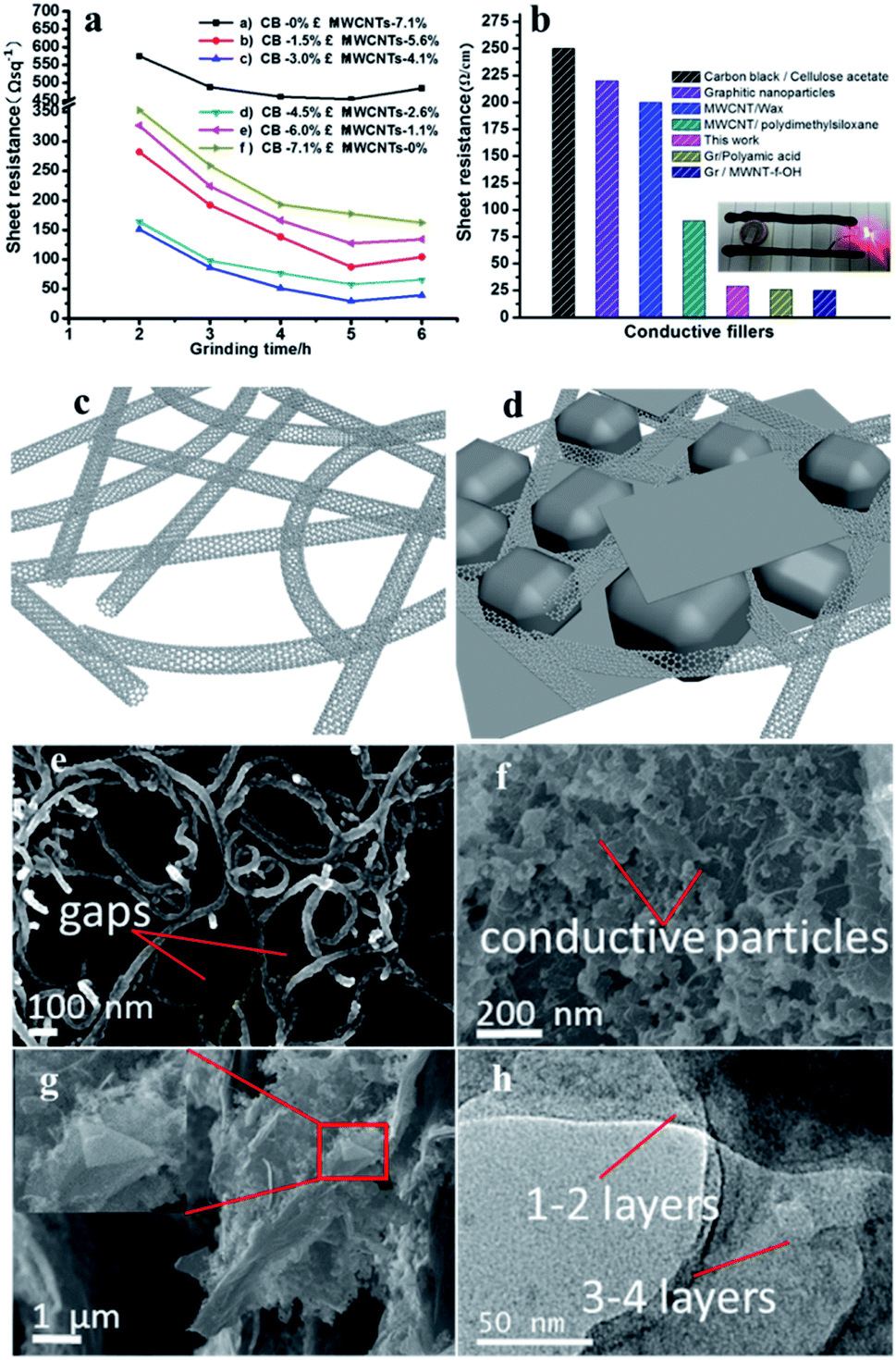 | ||
| Fig. 1 (a) Relationship between grinding time and sheet resistance of each group of conductive inks. (b) Comparison of conductivity of inks prepared by different conductive fillers. (c and d) Schematic diagram of CNTs network and graphite, CB filled CNTs network. (e) SEM image of the pure MWNT-f-OH, (f) SEM image of the CB, graphite and MWNT-f-OH are mixed conductive ink filled with each other. (g) SEM images of the cross-section of the ink layer. (h) TEM images of the few-layer graphene in ink. | ||
Preparation of printed capacitive sensing and performance testing
Sensing modules of different sizes and different ink areas were printed out with the prepared HCCA-inks by screen printer as shown in Fig. s7.†31–33 Proximity type capacitive sensing chip MTCH112 (ref. 31 and 34) was used to build a capacitive sensor with the printed conductive ink module group (see Fig. s7b†). As shown in Fig. s7c,† with the tester's hand, the maximum sensing height of different conductive ink modules was tested. According to the different usage scenarios of printed capacitive sensors, the most suitable ink sensing area graphics and area were determined.Characterization
The Raman spectroscopy was obtained by utilizing Confocal Raman Microspectroscopy RM 1000 Renishaw with an Ar+ laser excitation line at 515 nm. SEM observations were performed using an EVO MA10 (ZEISS). TEM images were obtained using a JEM2010 microscope operated at 200 kV. The conductive ink was uniformly printed on glass slides. After drying, the glass slides were mechanically snapped. The shape and cross-sectional thickness of the conductive ink adhered to the fracture surface of the glass slides were observed and measured. The power of the EL devices were measured by a precision power analyzer LMG610 (ZIMMER, USA).Results and discussion
Conductivity and morphology analysis
The resistance of conductive inks in each set was tested, as shown in Fig. 1a. Grinding made the conductive filler more evenly dispersed, when the grinding time was between 0–5 hours, the resistance of all the experimental groups decreased with the extension of grinding time. While the grinding time continued to increase, the resistance of the conductive inks increased, except for the f group. This may be due to the fact that the structure of the carbon nanotubes is destroyed as long-term mechanical polishing, so that the MWNT-f-OH in the electrically conductive fillers are degraded in the conductive properties due to the structure being destroyed. Fig. s8† shows the comparison of the structure of carbon nanotubes before and after grinding. It can also be seen from the Fig. 1a that when the mass fraction of graphite is 10.2% (the content of graphite is kept unchanged) CB, and MWNT-f-OH is respectively 3.0% and 4.1% the conductive ink has the best conductivity (Rs ≈ 29 Ω sq−1). The recent research focused on carbon conductive ink performance involving these materials are listed in Fig. 1b. The sheet resistance of CB/cellulose acetate,21 graphitic nanoparticles22 and CNTs/wax10 is too large to meet the requirements of some printed electronics, while Gr/MWNT-f-OH2,23 and Gr/polyamic acid24 have good electrical conductivity, but they are expensive, and it's difficult to meet industrial applications in large quantities. Therefore, a conductive ink with good electrical conductivity and relatively low price is expected to meet the needs of printed electronic products.As illustrated in Fig. s1c and d,† CNTs form the connection network, granular or flaky CB and graphite are used to fill the network gap, which not only reduces the use of carbon nanomaterials, but also maintains good electrical conductivity. Fig. 1e is a SEM image of the pure MWNT-f-OH, which reveals the gaps in the carbon nanotube ink. The gaps between the MWNT-f-OH causes a large electrical resistance, that's why the sheet resistance of the (a) group in Fig. 1a is the largest. The SEM image exhibited in Fig. 1f reveals CB, graphite and MWNT-f-OH in the conductive ink filled with each other. Conductive particles of graphite and CB fill in the space between the MWNT-f-OH, reducing the contact resistance between the conductive particles, thereby improving the conductivity of the ink. The carbon nanotube network also enhances the flexural resistance of the ink important for flexible electronics. The thickness of the cross-section of the ink layer is shown image in Fig. s2,† with an ink thickness of approximately 40 μm. The sheet resistance of the film made of the conductive ink was measured by four probes and a Keithley 2401 Source Meter. Fig. 1g is a zoom-in view of Fig. s2,† and it can be seen that the carbon materials in the ink cross-section structure are tightly bonded. It is noteworthy that a graphene-like structure was observed. Fig. 1h reveals a few-layered graphene35,36 in the ink. Raman spectroscopy37 was also conducted, as shown in Fig. 2, the 2D peak of graphite change with increased grinding time, it can be shown that during the preparation of the conductive ink, the mechanically exfoliated graphite produced graphene. As in the previous study proved that the dihydroxyphenyl functionalized MWNTs assist dispersibility of graphene in water is kinetically driven with the nanotube trapping between the graphene sheets or modification of graphene edges,2 so the MWNT-f-OH can easily disperse the graphene produced by grinding the graphite into the ink, which further enhances the conductivity of the ink.
 | ||
| Fig. 2 Raman spectrum of the graphite before grinding and few-layer graphene obtained from the ink after grinding. | ||
Mechanical analysis of paper – based flexible circuits
Printed flexible circuits are an important component for foldable electronics products.21,38,39 As shown in Fig. 3a, a flexible circuit was prepared by screen printing based on plain paper, the paper-base circuit is subjected to bending test, it can be seen that the resistance of the paper-based flexible circuit gradually increases as the bending angle θ increases, and it is worth mentioning that the change in resistance and the change in angle are approximately linear (R = 2.8286θ + 258.27). In order to further verify the reliability of the paper-based flexible circuit, we also performed repeated folding-resistant tests on the circuit. After folding 2000 times, the resistance value of the flexible circuit increased 11% (Fig. s3†). Due to the stability network structure of carbon nanotubes (Fig. 1c and d) and water-based acrylic resin connection, it can be seen that the conductive carbon materials are still connected after bending 2000 times (Fig. s4†). The linear relationship between the variation of the deformation of the flexible circuit and the resistance is potentially interesting. These result show potential for wearable electronic devices.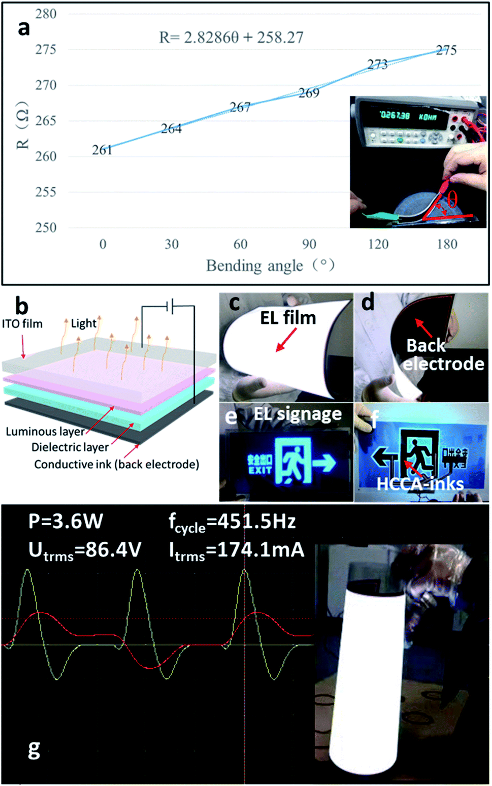 | ||
| Fig. 3 (a) Bending test of the paper-base flexible circuit and the relationship between resistance and bending angle of the paper-based flexible circuit. (b) The structure diagram of EL device. (c–f) EL devices prepared based on the HCCA-inks as a back electrode. (g) The power and performance parameters test of the EL devices. | ||
EL device performance analysis
In order to explore the application of the conductive ink, electroluminescent (EL) devices was prepared based on the HCCA-inks as a back electrode, and the power of the EL devices was measured by a precision power analyzer LMG610 (ZIMMER, USA) to be 4.0 mW cm−2. Fig. 3b is the structure diagram of EL device. Fig. 3c–f are the EL devices, one is a large size luminous device and the other is an EL signage which used ITO film or ITO glass as the positive electrode, and HCCA-inks as the back electrode. As shown in Fig. 3g, the power of the EL device with an area of 900 cm2 is 3.6 W, when the applied voltage, current, and frequency are 86.4 V, 174.1 mA, and 451.8 Hz, respectively, using the variable AC power to provide the required voltage and frequency (California Instruments, USA). Compared to the traditional industrial production of EL devices using silver paste as a back electrode, we demonstrate the use of HCCA-inks as the back electrode to produce EL devices, reducing costs and reducing environmental pollution.40Capacitance sensor performance analysis
A proximity type capacitive sensing chip MTCH112 (ref. 34 and 41) was used to build a capacitive sensor with the HCCA-inks. As shown in Fig. 4a–c and the ESI, Movie S1,† using HCCA-inks, a sensor block is drawn directly onto the paper, which is combined with the chip to form a sensor. The EL device lights up when the tester's hand is close to the sensor block, and goes off when the hand is away from the sensor. The maximum sensing height of different conductive ink modules was tested. According to the different usage scenarios of printed capacitive sensors, the most suitable ink sensing area graphics and area were determined. As can be seen from Fig. s4d–f,† three kinds of sensors with different structures were connected to the test device for testing. Multiple tests were performed to diminish errors and the maximum detection distance was recorded, the maximum detection distance: filling structure > spiral structure > ring structure (see Fig. 4h), but as can be seen from Fig. 4g, the printing area of the ring structure is the smallest. In general, the optimal design of the sensor is to make the printed area of the sensor as small as possible and the maximum detection distance as large as possible. In order to further explore the optimal design of the three structures (the printing area is equalized with the maximum detection distance) and to study the sensing performance of a given printed conductive area, we introduce a parameter, the detection coefficient α, defined as the maximum detection distance of the sensor dmax ratio to the total area of the conductive area as:41
 | (1) |
 | ||
| Fig. 4 (a–c) The construction and working principle of a simple proximity sensor. (d–f) Three kinds of sensors with different structures. (g) The printing area of the three kinds of sensors. (h) The maximum detection distance of the three kinds of sensors. (i) The detection coefficient α of the three kinds of sensors. (j) The maximum induction height of different printing size sensors with the same detection coefficient α. | ||
According to eqn (1), it can be seen that the larger the detection coefficient α, the higher the maximum detection distance of the conductive area per unit area, that is, the sensor performance of the unit area sensor is better. As can be seen from Fig. 4i, the detection coefficient α: ring structure (0.867) > spiral structure (0.394) > filling structure (0.258), the detection coefficient of the ring structure is much larger than the other two structures. As shown in Fig. 4j, different size sensors with the same detection coefficient α, the sensing height is linear with the sensor size and ink area. We also demonstrate a sensor with the 0.5 cm is a superior size, the maximum sensing height is 12 cm, which saves ink and has a relatively high sensing height (see Fig. s6†).
Conclusions
In conclusion, we have reported a new formula based on CB, graphite and carbon nanotubes as conductive fillers, with a waterborne acrylic resin as a linker for preparing conductive. The minimum sheet resistance is up to 29 Ω sq−1, with excellent conductivity and low cost. We demonstrated the preparation of paper-based flexible circuits with excellent mechanical stability and a linear relationship between deformation and resistance changes. After bending 2000 times to an angle of 180°, the resistance increased by 11%. The prepared HCCA-inks was used as the back electrode of a large-sized (900 cm2) EL device, and the power of the EL device was 4.0 mW cm−2, which's the first reported in previous studies. We also demonstrated the relationship between printed capacitive sensor shape, size, and printed area of conductive ink. In conclusion, we have prepared high-performance conductive inks using a simple method. The ink has excellent electrical conductivity and has excellent flex resistance when applied to flexible circuits. Replacement of silver paste as the back electrode of EL devices has also been tested. Here, we applied the prepared HCCA-inks to EL devices, printed capacitive sensors, and flexible bending circuits, it is a first demonstration.The methods described herein for making HCCA-inks can be further explored, such as testing of different conductive fillers, and conductive inks with different performance properties may be prepared. Moreover, the prepared conductive ink can be applied as the electrode of the thin film battery, for super capacitors, and for elastic fabric-based flexible circuit.
Conflicts of interest
There are no conflicts to declare.Acknowledgements
The authors are grateful to the following: the Yale Institute for Nanoscience and Quantum Engineering; the Center for Research on Interface Structures and Phenomena and Teacher of Wuhan University Test Center, China; the authors are also grateful to Dr Matthew Montgomery for the Raman of the graphite, Dr Yuanqiu Bu for provide the proximity type capacitive sensing chip MTCH112, Dr Zibing Li for the Screen printing technology analysis.References
- L. X. He and S. C. Tjong, J. Mater. Chem. C, 2016, 4, 7043–7051 RSC.
- V. Georgakilas, A. Demeslis, E. Ntararas, A. Kouloumpis, K. Dimos, D. Gournis, M. Kocman, M. Otyepka and R. Zboril, Adv. Funct. Mater., 2015, 25, 1481–1487 CrossRef CAS.
- Z. Tehrani, T. Korochkina, S. Govindarajan, D. J. Thomas, J. O'Mahony, J. Kettle, T. C. Claypole and D. T. Gethin, Org. Electron., 2015, 26, 386–394 CrossRef CAS.
- M. Santhiago, M. Strauss, M. P. Pereira, A. S. Chagas and C. C. B. Bufon, ACS Appl. Mater. Interfaces, 2017, 9(13), 11959–11966 CrossRef CAS PubMed.
- W. J. Hyun, O. O. Park and B. D. Chin, Adv. Mater., 2013, 25(34), 4729–4734 CrossRef CAS PubMed.
- K. S. Novoselov, V. I. Fal'ko, L. Colombo, P. R. Gellert, M. G. Schwab and K. Kim, Nature, 2012, 490, 192–200 CrossRef CAS PubMed.
- V. Georgakilas, J. A. Perman, J. Tucek and R. Zboril, Chem. Rev., 2015, 115, 4744–4822 CrossRef CAS PubMed.
- M. J. Allen, V. C. Tung and R. B. Kaner, Chem. Rev., 2010, 110, 132–145 CrossRef CAS PubMed.
- O. Garate, L. Veiga, A. V. Medrano, G. Longinotti, G. Ybarra and L. N. Monsalve, Mater. Res. Bull., 2018, 106, 137–143 CrossRef CAS.
- T.-H. Chen, Y.-C. Yeh and Y.-C. Liao, ACS Appl. Mater. Interfaces, 2018, 10, 24217–24223 CrossRef CAS PubMed.
- D. Pantea, H. Darmstadt, S. Kaliaguine and C. Roy, Appl. Surf. Sci., 2003, 217, 181–193 CrossRef CAS.
- C. Phillips, A. Al-Ahmadi, S. J. Potts, T. Claypole and D. Deganello, J. Mater. Sci., 2017, 52, 9520–9530 CrossRef CAS.
- H. Oxfall, G. Ariu, T. Gkourmpis, R. W. Rychwalski and M. Rigdahl, eXPRESS Polym. Lett., 2015, 9, 66–76 CrossRef.
- D. Yoo, J. Kim and J. H. Kim, Nano Res., 2014, 7(5), 717–730 CrossRef CAS.
- S. B. Park, M. S. Lee and M. Park, Carbon Lett., 2014, 15, 117–124 CrossRef.
- A. Wright, Circuit World, 2013, 39(4), 181–187 CrossRef CAS.
- L. X. He and S. C. Tjong, Nanoscale Res. Lett., 2013, 8, 132–139 CrossRef PubMed.
- S. Azoz, A. L. Exarhos, A. Marquez, L. M. Gilbertson, S. Nejati, J. J. Cha, J. B. Zimmerman, J. M. Kikkawa and L. D. Pfefferle, Langmuir, 2015, 31, 1155–1163 CrossRef CAS PubMed.
- Y. Hernandez, V. Nicolosi, M. Lotya, F. M. Blighe, Z. Y. Sun, S. De, I. T. McGovern, B. Holland, M. Byrne, Y. K. Gun'ko, J. J. Boland, P. Niraj, G. Duesberg, S. Krishnamurthy, R. Goodhue, J. Hutchison, V. Scardaci, A. C. Ferrari and J. N. Coleman, Nat. Nanotechnol., 2008, 3, 563–568 CrossRef CAS PubMed.
- V. Georgakilas, A. Kouloumpis, D. Gournis, A. Bourlinos, C. Trapalis and R. Zboril, Chem.–Eur. J., 2013, 19, 12884–12891 CrossRef CAS PubMed.
- M. Santhiago, C. C. Correa, J. S. Bernardes, M. P. Pereira, L. J. M. Oliveira, M. Strauss and C. C. B. Bufon, ACS Appl. Mater. Interfaces, 2017, 9, 24365–24372 CrossRef CAS PubMed.
- F. Hof, K. Kampioti, K. Huang, C. Jaillet, A. Derre, P. Poulin, H. Yusof, T. White, K. Koziol, C. Paukner and A. Penicaud, Carbon, 2017, 111, 142–149 CrossRef CAS.
- V. Georgakilas, A. Bourlinos, D. Gournis, T. Tsoufis, C. Trapalis, A. Mateo-Alonso and M. Prato, J. Am. Chem. Soc., 2008, 130, 8733–8740 CrossRef CAS PubMed.
- S. Sankar Nemala, P. Kartikay, R. K. Agrawal, P. Bhargava, S. Mallick and S. Bohm, Sol. Energy, 2018, 169, 67–74 CrossRef.
- A. Salim and S. Lim, Sensors, 2017, 17, 2593–2613 CrossRef PubMed.
- S. Rus, M. Sahbaz, A. Braun and A. Kuijper, Lecture Notes in Computer Science, 2015, 9425, 77–92 CrossRef.
- J. Volf, V. Novak and V. Ryzhenko, Procedia Eng., 2015, 120, 200–205 CrossRef CAS.
- X. Q. Liao, Q. L. Liao, X. Q. Yan, Q. J. Liang, H. N. Si, M. H. Li, H. L. Wu, S. Y. Cao and Y. Zhang, Adv. Funct. Mater., 2015, 25, 2395–2401 CrossRef CAS.
- I. N. Kholmanov, C. W. Magnuson, A. E. Aliev, H. F. Li, B. Zhang, J. W. Suk, L. L. Zhang, E. Peng, S. H. Mousavi, A. B. Khanikaev, R. Piner, G. Shvets and R. S. Ruoff, Nano Lett., 2012, 12, 5679–5683 CrossRef CAS PubMed.
- S. Azoubel, S. Shemesh and S. Magdassi, Nanotechnology, 2012, 23, 344003 CrossRef PubMed.
- Y. Wei, R. Torah, Y. Li and J. Tudor, Sens. Actuators, A, 2016, 247, 239–246 CrossRef CAS.
- C. Cho and Y. Ryuh, Sens. Actuators, A, 2016, 237, 72–80 CrossRef CAS.
- P. He, R. J. Brent, H. Ding, J. Yang, D. J. Lewis, P. O. Brien and B. Derby, Nanoscale, 2018, 10, 5599–5606 RSC.
- Microchip datasheet, MTCH112 Dual-channel Proximity/touch Controller, 2016, available at: http://ww1.microchip.com/downloads/en/DeviceDoc/41668A.pdf.
- L. Huang, D. Zhang, F. H. Zhang, Z. H. Feng, Y. D. Huang and Y. Gan, Small, 2018, 14, 1704190 CrossRef PubMed.
- A. Ciesielski, S. Haar, M. El Gemayel, H. Yang, J. Clough, G. Melinte, M. Gobbi, E. Orgiu, M. V. Nardi, G. Ligorio, V. Palermo, N. Koch, O. Ersen, C. Casiraghi and P. Samori, Angew. Chem., Int. Ed., 2014, 53, 10355–10361 CrossRef CAS PubMed.
- D. Nuvoli, V. Alzari, R. Sanna, S. Scognamillo, M. Piccinini, L. Peponi, J. M. Kenny and A. Mariani, Nanoscale Res. Lett., 2012, 7, 674–683 CrossRef PubMed.
- Y. H. Jung, T. H. Chang, H. Zhang, C. Yao, Q. Zheng, V. W. Yang, H. Mi, M. Kim, S. J. Cho, D. W. Park, H. Jiang, J. Lee, Y. Qiu, W. Zhou, Z. Cai, S. Gong and Z. Ma, Nat. Commun., 2015, 6, 7170–7181 CrossRef PubMed.
- R. Z. Li, A. M. Hu, T. Zhang and K. D. Oakes, ACS Appl. Mater. Interfaces, 2014, 6, 21721–21729 CrossRef CAS PubMed.
- S. Sato, T. Shimizu and M. Ohuchi, J. Soc. Inf. Disp., 2019, 27, 3–12 CrossRef CAS.
- Y. Wei, R. Torah, Y. Li and J. Tudor, Sens. Actuators, A, 2016, 247, 239–246 CrossRef CAS.
Footnote |
| † Electronic supplementary information (ESI) available. See DOI: 10.1039/c9ra01721f |
| This journal is © The Royal Society of Chemistry 2019 |