
 Open Access Article
 This Open Access Article is licensed under a Creative Commons Attribution-Non Commercial 3.0 Unported Licence
Efficient air-stable perovskite solar cells with a (FAI)0.46(MAI)0.40(MABr)0.14(PbI2)0.86(PbBr2)0.14 active layer fabricated via a vacuum flash-assisted method under RH > 50%†
Li Chenab,
Hui Cao *a,
Shurong Wanga,
Yuxing Luob,
Tao Taoa,
Jinwei Suna and
Mingdao Zhang*a
*a,
Shurong Wanga,
Yuxing Luob,
Tao Taoa,
Jinwei Suna and
Mingdao Zhang*a
aDepartment of Chemistry, Jiangsu Key Laboratory of Atmospheric Environment Monitoring and Pollution Control, Collaborative Innovation Center of Atmospheric Environment and Equipment Technology, School of Chemistry and Materials, Nanjing University of Information Science & Technology, Nanjing 210044, Jiangsu, PR China. E-mail: yccaoh@hotmail.com; matchlessjimmy@163.com
bInstitute of Functional Nano & Soft Materials, Soochow University, Soochow 215123, PR China
First published on 1st April 2019
Abstract
In this work, we present a new kind of perovskite, (FAI)0.46(MAI)0.40(MABr)0.14(PbI2)0.86(PbBr2)0.14, the vacuum flash-assisted solution processing (VASP) of which can be carried out under relative humidity (RH) higher than 50% in ambient air. The smooth and highly crystalline perovskite showed a maximum PCE of 18.8% in perovskite solar cells. This kind of perovskite was demonstrated to be of good stability in ambient air. Holes and electrons have larger and more balanced diffusion lengths (643.7/621.9 nm) than those in the MAPbI3 perovskite (105.0/129.0 nm) according to the PL quenching experiment. The role of incorporating a large amount of MA+ cations to stabilize the intermediate phase via VASP under high RH is attributed to their better ability to intercalate into the sharing face of the one-dimensional face-sharing [PbI6] octahedra, forming the three-dimensional corner-sharing form. Moreover, hole/electron transfer times at the perovskite/Spiro-OMeTAD (PCBM) interfaces (8.90/9.20 ns) were found to be much larger than those in the MAPbI3 perovskite (0.75/0.40 ns), indicating that there still is enormous potential in further improving the performance of this kind of perovskite solar cell by interfacial engineering.
Introduction
Hybrid inorganic–organic halide perovskite exhibits unique optoelectronic properties, such as long carrier diffusion length,1 tunable bandgap,2 ambipolar carrier diffusion properties,3 and with good polycrystalline mineralization under low temperature and via a simple preparation method.4–6 All these advantages boosted the development of the state-of-the-art perovskite solar cells (PSCs), the power conversion efficiency (PCE) of which has increased from 3.8% to 22.1% during the past decade.7–10 However, PSCs are still facing the challenges of poor stability to moisture during fabrication and storing processes in spite of their high solar-to-electric conversion efficiency.7,11Multi-compound (MC) perovskites, especially, (FAI)0.81(MABr)0.15(PbI2)0.85(PbBr2)0.15, have achieved much better performance than the simple MAPbI3 or FAPbI3 (FA: formamidinium, MA: methylammonium). Compared to the conventional MAPbI3, the MC-perovskite can enhance the moisture tolerance and thermal stability greatly.12–16 Apart from the stability, the bandgap of this kind of perovskite is also narrower than MAPbI3, making it as one of the ideal candidates that could utilize more solar energy according to Shockley–Queisser (S–Q) theory.17 The improvements in optoelectronic properties are caused by FAPbI3 component, which has a better bandgap, 1.48 eV, relative to that of MAPbI3 (1.57 eV), allowing more solar absorption in near infrared (NIR) spectrum.5,17
The stability was attributed to the simultaneous incorporation of MA+ cations and Br− anions into the FAPbI3. Moreover, films of this mixed perovskite on substrate are dense and uniform, overcoming the shortage of the pure FAPbI3 film with pinholes and a rough surface.18–20 Another shortage of the pure FAPbI3 is the inexpectant existence of a yellow non-perovskite phase (δ-FAPbI3), which shows poor optoelectronic properties. Transformation of this δ-FAPbI3 to black α-FAPbI3 phase that we need should be thermally treated over 170 °C.21 And this process does not proceed thoroughly, unless the FAI and PbI2 take a fractional steps reaction. The incorporation of MA+ into FAPbI3-based perovskite precursor, essentially changes the mechanism of crystal nucleation, and efficiently gets rid of the δ-FAPbI3.
According to general cognition, the mono-A-cation perovskite (ABX3) has poor stability in ambient air. The perovskite crystal suffers from the degradation because of the reaction between H2O and the organic iodides.22–27 The dramatic degradation of MAPbI3 in air with high relative humidity about 50% was reported by Divitini and co-workers.28 In addition, Yun and co-workers also investigated the FAPbI3 degradation through the grain boundaries with humidity. The results demonstrated that the α-FAPbI3 perovskite ultimately turned into hexagonal yellow non-perovskite δ-FAPbI3 in different humidity conditions, because the humidity easily seeps into the grain boundaries.29,30 In contrast, the mixed (FAPbI3)1−x(MAPbBr3)x can form a stable perovskite as well as a high power conversion efficiency.
Many fabrication methodologies of the MC-perovskite such as anti-solvent, recrystallization, and vacuum flash-assisted solvent processing produced highly efficient PSCs. Either anti-solvent or other vacuum free preparation methods were substantially affected by skills of operators. In contrast, the VASP method was impressive because of its better reproducibility with a much narrower distribution of PCEs, which is the necessary requirement that should be met in the future industrial production. With this technique, Li et al. fabricated the high-quality perovskite with 15% FAPbI3 substituted by MAPbBr3 at low temperature and obtained the high PCE up to 20.5% with perfect distribution in device area exceeding 1 cm2.31
However, it was also noticed that the VASP needs to be prepared in an environment with a low RH.31 The strict conditions hinder the reappearance of this mixed perovskite under high RH. In the process of vacuum-flash assisted fabrication with RH larger than 50%, the (FAI)0.81(MAI)0.15(PbI2)0.85(PbBr2)0.15-DMSO (N,N-dimethyl sulfoxide) film on meso-TiO2 substrate quickly changes into a yellow and vague phase, not the expected transparent brown intermediate phase. And the corresponding perovskite films show little optoelectronic activity.
Since the immanent properties of perovskite can affect the performance of ultimate PSCs,32–40 the way of mineralization of perovskite is thus essential to the device. In this work, the MC-perovskite with the new formula of (FAI)0.46(MAI)0.40(MABr)0.14(PbI2)0.86(PbBr2)0.14 was investigated in the framework of VASP under RH as high as 55% (if not specially mention in the following, MC-perovskite refers to this formula). A film of expected transparent and orange intermediate phase was obtained during the vacuum-flash process. Accordingly, PCE of the solar cell with this MC-perovskite film has reached 18.8% with a narrow distribution. PSCs also demonstrated a long-term stability in the test over 500 hours.
Results and discussion
Architecture and performances of PSCs
As shown in Fig. 1a, the architecture of PSCs applied in our experiments comprises the FTO contact, compact-TiO2 (C-TiO2) and mesoporous TiO2 (M-TiO2) electron extracting layer, perovskite light-absorption layer, and Spiro-OMeTAD hole extracting layer. The meso-architecture is generally believed as an efficient way to improve the PCE of PSCs because the contact area between perovskite and mesoporous TiO2 layer is greatly enhanced, facilitating the interfacial electron extraction.41,42 Fig. 1b shows the cross-sectional field effect scanning electron microscopy (SEM) image of the holonomic perovskite device. The FTO front face is covered with a 30 nm C-TiO2 layer, a 200 nm M-TiO2 layer, a 370 nm perovskite capping layer, a 160 nm hole extracting layer and an 80 nm Au electrode in sequence.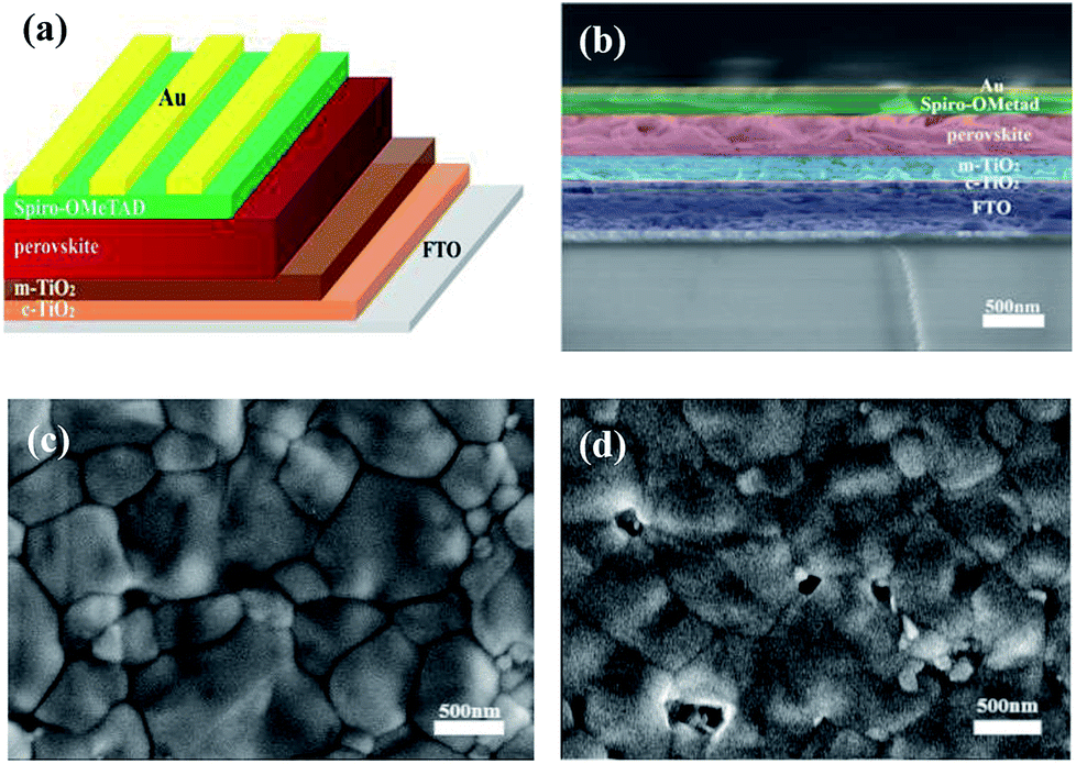 | ||
| Fig. 1 The architecture of perovskite solar cell and morphology of perovskite film which was deposited on the substrate of FTO/C-TiO2/M-TiO2. (a) Scheme of the investigated perovskite solar cell. (b) A cross-sectional SEM image of the complete perovskite solar cell. (c) The top-view SEM of (FAI)0.46(MAI)0.40(MABr)0.14(PbI2)0.86(PbBr2)0.14 perovskite film, and (d) MAPbI3 perovskite film. | ||
γ-Butyrolactone (GBL) was taken as a cosolvent with N,N-dimethyformamide (DMF) and dimethyl sulfoxide (DMSO) in preparing the MC-perovskite precursor. Incorporation of GBL can effectively reduce the speed of crystal nucleation, facilitating the formation of a dense and uniform perovskite film without pinholes.43 Spin-coating of MC-perovskite precursor was performed in the ambient air and then transferred into the vacuum chamber. The intermediate (FAI)0.46(MAI)0.40(MABr)0.14(PbI2)0.86(PbBr2)0.14-DMSO film via VASP under the pressure of 20 Pa after 15 seconds is light brown and transparent. While the (FAI)0.81(MABr)0.15(PbI2)0.85(PbBr2)0.15-DMSO film quickly turns into a yellow and vague intermediate phase, which is possibly due to the crystallization of PbI2 or the formation of δ-FAPbI3. It should be noted that when the proportion of FAI is higher than 0.46 then the intermediate phase becomes to be instable under larger RH, leading to a yellow and vague phase. After annealing, the MC-perovskite film shows a dark brown, mirror-like surface. The SEM images of perovskite films of (FAI)0.46(MAI)0.40(MABr)0.14(PbI2)0.86(PbBr2)0.14 and MAPbI3 are shown in Fig. 1c and d, respectively. The MC-perovskite contains bigger, neat and close-knit grains compared with the MAPbI3 perovskite. Many pinholes and small crystallites exist in MAPbI3 perovskite, leading to a strong non-radiative recombination of charge carriers because of the increase of the grain boundary.44,45
To further investigate the (FAI)0.46(MAI)0.40(MABr)0.14(PbI2)0.86(PbBr2)0.14 crystal, some comparison tests between MAPbI3 and this kind of MC-perovskite mineralized via VASP method were carried out. In Fig. 2a, we show the ultraviolet-visible absorption spectra (UV-VIS) of MAPbI3 and this MC-perovskite on the substrate of FTO glass. It demonstrates that the onset of absorption of the MC-perovskite is at the wavelength a little longer than that of MAPbI3 perovskite, in consistent to the fact that the energy gap of MC-perovskite is smaller than that of MAPbI3 perovskite. The plateaus and the rapid rising parts in the range of 780 nm to 450 nm of the MC-perovskite are generally higher than those of the MAPbI3 perovskite, indicating the better light absorption of the MC-perovskite. This better light absorption is attributed to the existence of 46% FAPbI3 in the MC-perovskite. Fig. 2b shows the steady-state photoluminescence (PL) spectra of the MC-perovskite and the MAPbI3 perovskite. The PL peak of the MC-perovskite is at 774.3 nm and that of the MAPbI3 perovskite is at 768.3 nm. The red-shift of steady-state PL peak of the MC-perovskite compared to the MAPbI3 perovskite is in consistent to their red-shift of the onset at the absorbance spectra. The luminescence strength of MC-perovskite is also stronger than that of the MAPbI3 perovskite, and accordingly, the integration of the PL curve of the MC-perovskite is larger than that of the MAPbI3 perovskite, implying that more charge carriers are photogenerated in the MC-perovskite.
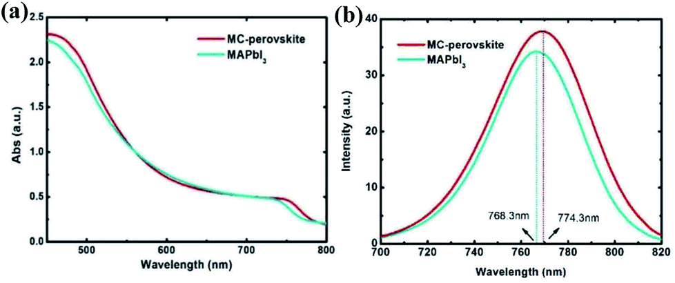 | ||
| Fig. 2 (a) The UV-VIS curves of two kinds of perovskite films which were fabricated by the same VASP method. (b) The steady-state PL measurement of MC-perovskite and MAPbI3 perovskite. | ||
Fig. 3a shows the average cell performance with the MC-perovskite and the MAPbI3 perovskite active layers (corresponding IPCE see Fig. S1†). The PCE of 17.60% of the MC-perovskite solar cell is much higher than that of the MAPbI3 perovskite solar cell, which is 15.00%. The MC-perovskite solar cell has a short-circuit current (Jsc) of 23.03 mA cm−2, open-circuit voltage (Voc) of 1.10 V, and fill factor of 69.47%, in contrast to the MAPbI3 perovskite solar cell with the short-circuit current 21.69 mA cm−2, open-circuit voltage of 1.03 V, and with fill factor of 67.14%. Each parameter of the MC-perovskite solar cell is better than that of MAPbI3 perovskite solar cell. As shown in Fig. 3b, the best MC-perovskite solar cell exhibits the PCE of 18.80% with the open-circuit voltage of 1.12 V, the short-circuit current of 22.45 mA cm−2, and the fill factor of 74.78%. However, in both Fig. 3a and b, we find that shunt-resistance of PSCs does not tend to infinity, which is probably due to the thickness mismatch in terms of the electron (or hole) extracting layers.
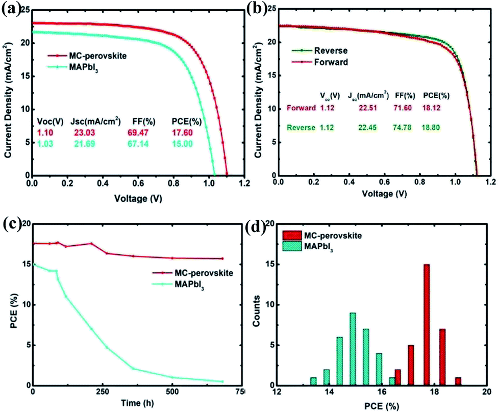 | ||
| Fig. 3 Performances of MC-perovskite and MAPbI3 perovskite solar cells fabricated via VASP method. (a) Average J–V curves of MC-perovskite and MAPbI3 perovskite solar cells. (b) J–V curves of the best one of MC-perovskite solar cells. (c) The power conversion efficiency decay. (d) Distributions of PCE for two kinds of perovskite solar cells. | ||
Hysteresis in PSCs has attracted intensive discussions and many mechanisms were proposed.31,46 Hysteresis effect in the MC-perovskite solar cells, as seen in Fig. 3b, is not remarkable. The difference of PCE between the reverse scanning and the forward scanning is only 0.68%. It is probably because of the balanced diffusion lengths between the electron and the hole, as will be discussed in the next subsection. And the MC-perovskite solar cells also demonstrate good stability, as shown in Fig. 3c. The 680 hours test on the MC-perovskite solar cell stored in a dry Petri dish shows the decay of about 11% in PCE. We find that decay of Voc is negligible, while that of short-circuit current (Isc) and fill factor (FF) is dominant, which is in consistent with the previous report.47 In contrast, the MAPbI3-perovskite solar cell shows the obvious decay in PCE after 100 hours, due to the degradation of the MAPbI3 perovskite.
To investigate the parallelism of the perovskite solar cells prepared with this method, we made stochastic statistics on 30 devices to check its distribution. Fig. 3d shows a much better distribution in the PCE of the MC-perovskite solar cells than that of the MAPbI3 perovskite solar cells. The center of the distribution of the MC-perovskite solar cells is located at 17.6% while that of the MAPbI3 is only located at about 15.0%.
The effect of chlorine passivation of the interfacial defect states, acting as the non-radiative recombination sites, has been reported by Tan et al.48 recently. In their work, the compact TiO2 layer is modified by the chloroform to realize the interfacial passivation in the planar PSCs. In our approach, small amount of MACl is directly doped into the precursor. Thus, on the one hand, MACl could passivate the interface between the MC-perovskite and the mesoporous TiO2; on the other hand, MACl might modify the crystal nucleation process. We believe that the passivation effect plays the most important role, since there is no apparent difference in the appearance of the MC-perovskite films with and without the incorporation of MACl.
Interfacial separation and transport of charge carriers
We combined photoluminescence-quenching (PL-quenching) experiments with the one-dimensional diffusion dynamics simulations to investigate the interfacial separation and transport of photogenerated charge carries in the MC-perovskite solar cells.The PL-quenching experiment is sketched in Fig. 4a. The samples were photo-excited from the side of glass substrate. PC61BM and Spiro-OMeTAD are often utilized as the electron-quenching and the hole-quenching layer. It is assumed that all photogenerated charge carriers are quenched when they reach the interface between perovskite and electron- or hole-extracting layer. A sample SEM image of perovskite with quenching layer is shown in Fig. 4b. A perovskite layer is at first deposited on the glass substrate, and then the quencher of PC61BM or Spiro-OMeTAD is applied to fabricate a heterojunction.
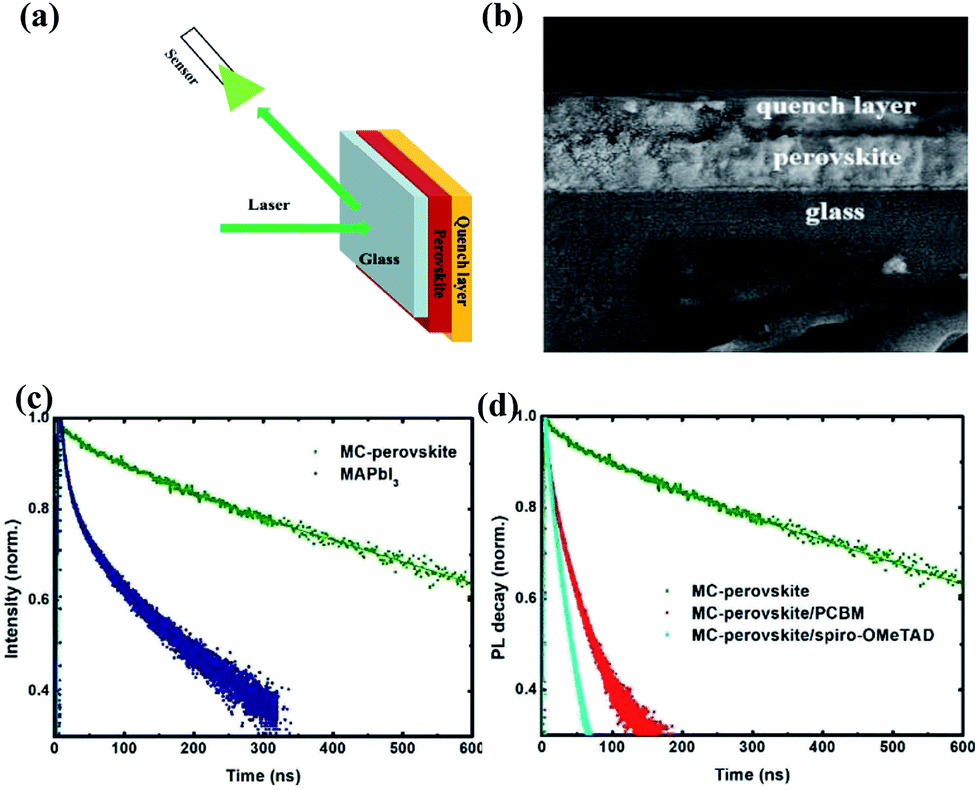 | ||
| Fig. 4 (a) The schematic sketch of diffusion length measurement. (b) The cross-sectional SEM image of perovskite and quenching layer. (c) The time-resolved PL measurement of MC-perovskite and MAPbI3 perovskite on the substrate of glass. (d) The time-resolved PL measurement of MC-perovskite and MC-perovskite with different quenching layers. | ||
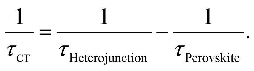
In order to estimate the interfacial charge separation and charge transport, we should get the charge transfer (CT) time at interfaces and the charge diffusion length in the perovskite layer. For this purpose, we first investigate the charge recombination lifetime of photo-generated charge carriers in the perovskite layer. As shown in Fig. 4c, the time-resolved PL spectra of the MC-perovskite and MAPbI3 perovskite that are deposited on the glass substrate in absence of a quencher are obtained. Recombination lifetimes of the MC-perovskite and the conventional MAPbI3 perovskite are 276.3 ns and 9.6 ns respectively, indicating that the recombination rate of the MC-perovskite is much smaller than that of the MAPbI3 perovskite.
Then, we investigate the recombination lifetime of photo-generated excitons in the perovskite/quencher heterojunctions. From Fig. 4d, we find that the recombination lifetimes of charge carriers in the MC-perovskite/PC61BM and MC-perovskite/Spiro-OMeTAD are 8.9 ns and 8.6 ns, respectively. With the lifetimes of charge carries in the perovskite layer and the heterojunctions, we can calculate the interfacial charge transfer time and the charge diffusion length in perovskite layer as following49
 | (1) |
As shown in Table 1, the charge transfer times at the MC-perovskite/PC61BM and the MC-perovskite/Spiro-OMeTAD interfaces are 9.20 ns and 8.90 ns, respectively. These values are about dozens of times larger than those at MAPbI3-perovskite/PC61BM (0.40 ns) and MAPbI3-perovskite/Spiro-OMeTAD (0.75 ns) interfaces. This apparently indicates that the resistances for charge carriers passing through the MC-perovskite/PC61BM and the MC-perovskite/Spiro-OMeTAD interfaces are much larger than those through the MAPbI3/PC61BM and MAPbI3/Spiro-OMeTAD interfaces. This result implies that more efforts need to be put into the following two aspects to improve the PCE of MC-perovskite solar cells in the future. One is to synthesize more efficient electron- or hole-extracting materials, and the other is to reduce the contact resistance further via the interfacial modification. We believe that this is more important for the MC-perovskite solar cells than for the MAPbI3-perovskite solar cells.
| Perovskite | Species | D (nm2 ns−1) | LD (nm) | τCT (ns) |
|---|---|---|---|---|
| MC-perovskite | Electron | 1400 | 621.9 | 9.20 |
| Hole | 1500 | 643.7 | 8.90 | |
| MAPbI3 (ref. 50) | Electron | 1700 | 129.0 | 0.40 |
| Hole | 1100 | 105.0 | 0.75 |
The diffusion lengths for photogenerated charge carriers in the perovskite can be calculated by one-dimensional diffusion equation50
 | (2) |
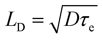 , where τe is the lifetime of charge carries in perovskite.
From Table 1, it can be seen that MC-perovskite has larger and similar LD for electron and hole. The diffusion lengths for both electron and hole in this perovskite are more than 620 nm, which is beyond the width of perovskite films applied in device (about 570 nm). In contrast, it was shown that the diffusion lengths of electron and hole in MAPbI3 perovskite are only about 129 nm and 105 nm, respectively. Thus, in the MC-perovskite, the diffusion length of charge carriers can ensure electrons (holes) travelling to the electron (holes)-extracting interface before recombination. Moreover, the balanced diffusion length of the electron and the hole might effectively reduce the local polarization due to the accumulation of one kind of charge carrier, ensuring the dynamical contribution to the hysteresis during operation as less as possible.
The role of MAI in stabilizing the intermediate phase under high humidity during VASP
Collapse of the intermediate phase of (FAI)0.81(MABr)0.15(PbI2)0.85(PbBr2)0.15-DMSO under large RH in the ambient air hampers the fabrication of high quality perovskite film. However, partial FAI in this perovskite is substituted by MAI to get the (FAI)0.46(MAI)0.40(MABr)0.14(PbI2)0.86(PbBr2)0.14 MC-perovskite, which shows better endurance of RH in VASP.In order to understand the mechanism of the stabilization of the intermediate phase via the remarkable substitution of FAI with MAI, we firstly tried to figure out what process happens in producing the yellow and vague film during VASP of the former perovskite with higher humidity in the environment. Because of the amorphous form of this vague film, XRD tests cannot be carried out. Hence, we propose the reasonable hypothesis in the following. The first probable process may be the crystallization of the PbI2 during the VASP. However, we believe that another more complicated process may happen. Because PbI2, FAI, and DMSO preferentially form the Lewis acid–base adduct, PbI2·FAI·DMSO, in which the base, FAI, coordinates with the Lewis acid, PbI2. Due to the stoichiometric addition of DMSO, this adduct can act as the stable intermediate phase in both anti-solvent and VASP fabrication methodologies. However, moisture has been found as one of the origination that induces the severe damage of the black perovskite phase α-FAPbI3, leading to the formation of the yellow non-perovskite δ-FAPbI3. In fact, the yellow δ-FAPbI3 with hexagonal symmetry (space group P63mc) should be more stable than the black α-FAPbI3 with trigonal symmetry (P3m1), because the δ-FAPbI3 has an energy gap (2.43 eV) wider than the α-FAPbI3 (1.48 eV).51 Moreover, the yellow δ-FAPbI3 is favorable in the low temperature which is the result of drastic solvent volatilization during the vacuum flash process. And it entails a temperature as high as 170 °C to change the yellow δ-FAPbI3 to the black α-FAPbI3, indicating the existence of a higher potential barrier for this phase transition. Hence, to a large extent, the yellow and vague intermediate phase film observed during VASP can be attributed to the formation of the yellow non-perovskite δ-FAPbI3.
Although the collapse of the intermediate film is observed to be triggered in the step of vacuum flash, the reason behind should be the absorption of water molecules in the previous spin-coating step. DMSO has strong water absorption capability, and thus large amount of water molecules can enter into the precursor film during spin-coating process in an ambient humid atmosphere, especially in the case of large centimeter-scale surface area with respect to the thin nanoscale film. The PbI2·FAI·DMSO adduct could be partially destroyed because of the formation the hydrogen bond between the water molecules and DMSO. In fact, the iodine coordinates to Pb2+, leading to the formation of [PbI6]4− octahedron microstructure. The loss of DMSO due to the competitive combination by water molecules makes it aggregate into one-dimensional linear chains with face-sharing, facilitating the formation of δ-FAPbI3.51
The substitution of FA+ with MA+ essentially changes the connection behavior among the [PbI6]4− octahedrons. The small size of MA+, in contrast to FA+, facilitates its intercalating into the sharing face, with the resultant spatial configuration as a three-dimensional corner-sharing [PbI6]4− octahedrons network.52 This process doesn't change a lot even if the absorption of water molecules in the step of spin-coating of the precursor. This three-dimensional network acts as the framework for suitable size A site cations, forming the final perovskite film without great volume change. In our experiments, we found that the mole FA+/MA+ ratio of about 46![[thin space (1/6-em)]](https://www.rsc.org/images/entities/char_2009.gif) :54 can generate the perfect transparent intermediate phase in VASP in the ambient air with RH < 55%.
:54 can generate the perfect transparent intermediate phase in VASP in the ambient air with RH < 55%.
X-ray diffraction (XRD) spectrum of the MC-perovskite (fabricated in ambient air) showed in Fig. 5a gives further insight into the perovskite crystal. We find three main diffraction peaks that are centered at 14.08°, 28.60°, and 32.00°, respectively. The intense peak located at 32.00° is the characteristic of the α-FAPbI3 (![[2 with combining macron]](https://www.rsc.org/images/entities/char_0032_0304.gif) 31/
31/![[1 with combining macron]](https://www.rsc.org/images/entities/char_0031_0304.gif) 23). Moreover, peaks centered at 28.60° and 32.00° are very intense (while for MAPbI3, as shown in Fig. 5b, they are weak), which can be assigned to cooperative effect of the complex (FA)x(MA)1−xPbI3. The absence of typical peak of PbI2 (12.23°) illustrates that there are not too much remnant PbI2 in our perovskite because of the equal stoichiometric ratios guaranteed by the one-step deposition methodology. The image also reveals that large perovskite grains in the film according to the intensity and spike of peaks, in agreement with the SEM tests. Most importantly, no peak of the non-perovskite δ-FAPbI3 (11.60°) exists, indicating that the channel of one-dimensional face-sharing [PbI6]4− octahedrons is blocked with the addition of MAI, even in the highly humid ambient air.
23). Moreover, peaks centered at 28.60° and 32.00° are very intense (while for MAPbI3, as shown in Fig. 5b, they are weak), which can be assigned to cooperative effect of the complex (FA)x(MA)1−xPbI3. The absence of typical peak of PbI2 (12.23°) illustrates that there are not too much remnant PbI2 in our perovskite because of the equal stoichiometric ratios guaranteed by the one-step deposition methodology. The image also reveals that large perovskite grains in the film according to the intensity and spike of peaks, in agreement with the SEM tests. Most importantly, no peak of the non-perovskite δ-FAPbI3 (11.60°) exists, indicating that the channel of one-dimensional face-sharing [PbI6]4− octahedrons is blocked with the addition of MAI, even in the highly humid ambient air.
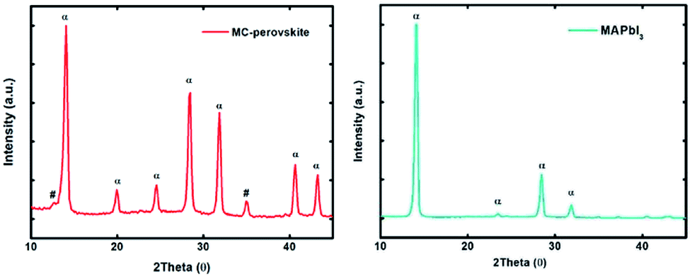 | ||
| Fig. 5 X-ray diffraction spectra of powders of the (a) MC-perovskite and (b) MAPbI3 perovskite. | ||
Conclusions
In summary, new perovskite, (FAI)0.46(MAI)0.40(MABr)0.14(PbI2)0.86(PbBr2)0.14, with larger amount of MAI incorporated, can efficiently reduce the humidity sensitivity of perovskite fabrication via VASP in ambient air environment with RH > 50% and improve the parallelism of perovskite solar cells. PSCs based on the modified perovskite not only have improved stability, but also have good power conversion efficiency (with best one as 18.8%) and less hysteresis effect. Diffusion lengths of both holes and electrons were found to be long enough for their transport across the perovskite layer to arrive at the perovskite/HTL (ETL) interfaces. Charge transfer at perovskite/HTL (ETL) interfaces was also investigated using PL spectra. Finally, the role of MA+ cations in stabilizing the intermediate phase under high humidity during VASP was discussed. It is believed that large amount of MA+ cations can efficiently change the one-dimensional face-sharing [PbI6], which is the origin of the formation of δ-phase perovskite, into its three-dimensional corner-sharing form even under the high RH and facilitate the formation of α-phase perovskite.Experimental
Materials
Methylammonium-iodide (MAI) (98%), formamidine-iodide (FAI) (98%), γ-butyrolactone (GBL) (98%), PbBr2 (98%) and methylamine bromine (98%) were all purchased from Macklin. PbI2 (99%) was purchased from Polymer light technology Co., China. Dyesol-30NRT and Spiro-OMeTAD was purchased from Youxuan Co., Ying Kou, China. Other commonly used solvents and materials were used as received in laboratory.Device fabrication
FTO glasses (Pilkington TEC A7 7Ω) were cleaned in ultrasonic bath containing glass detergent solution, isopropanol and ethanol in sequence. The substrates were then treated in UV–O3 after being dried. A compact TiO2 layer was prepared by spin-coating the diluted 0.14 M titanium diisopropoxide dis(acetylacetonate) (in n-butyl alcohol) on the substrate at 2000 rpm for 30 s, which was followed by drying at 120 °C for 10 min. Then the substrate was sintered on a hot plate at 500 °C for 40 min. After cooling to room temperature, a diluted mesoporous TiO2 films prepared using a TiO2 paste (Dyesol 30-NRD) in ethanol solution was spin-coated on the cooled substrate at 3500 rpm for 30 s. The spin-coated substrate was then thermally treated at 500 °C for 40 min. The perovskite precursor solution was prepared with 1.4 M (FAI)0.46(MAI)0.40(MABr)0.14(PbI2)0.86(PbBr2)0.14, and additional MACl (0.1 M) in a mixed solution with the molar ratios of DMF:GBL = 1:2, DMSO:PbX2 = 1:1. The precursor solution was then spin-coated on the substrates with 1000 rpm for 18 s, 4000 rpm for 18 s. The substrates were quickly transferred into a small vacuum chamber, in which the pressure was then immediately dropped below 20 Pa for 15 s. Subsequently the substrate was taken out of the chamber after recovering to normal atmosphere pressure and quickly put on the hot plate at 110 °C for 10 min in air environment. After cooling down to room temperature, the hole-transport layer was spin-coated on the substrate at 3000 rpm for 30 s. The hole-transport solution was prepared by dissolving 64 mg Spiro-OMeTAD, 8 mg spiro-TFSI, and 28 μl tert-butylpyridine in 1 ml chlorobenzene. Finally, 80 nm of gold was deposited by thermal evaporation using a shadow mask to match the electrode.
Characterization
All processes were carried out in an ambient air without any control of relative humidity. The morphology of perovskite films and cross-sectional view were observed by a SEM (HITACHI S-4800). XRD spectra of perovskite crystal were measured by X-ray diffraction spectrometry (Shimadzu XRD 6100). Absorption spectra of perovskite on glass were measured by an ultraviolet-visible spectrophotometer (Cary 3100) in a wavelength range at 200–800 nm at room temperature. Steady-state and time-resolved PL spectra were obtained using a time-correlated single photon counting setup (FluoTime 300, PicoQuant GmbH) with a 530 nm laser as the excitation source, pulsed at a frequency of 0.58 MHz. Photocurrent-voltage (J–V) characteristics of solar cells were measured under 100 mW cm−2 (AM 1.5G one Sun) illumination with 450 W Xenon lamp (Newport SLF049). Standard silicon cell was used to calibrate the light intensity. The scan rate was 0.1 V s−1. The active area of perovskite solar cell was 0.1 cm2. IPCE was measured by a QE/IPCE system (Newport) in the wavelength of 300–800 nm at room temperature.Conflicts of interest
There are no conflicts to declare.Acknowledgements
This work was supported by grants from the National Natural Science Foundation of China (No, 21473092, 21501097), Nanxin Pharm Co., Ltd., Nanjing, the Natural Science of Foundation of Jiangsu Province (No. BK20150890, BK20170939), and the Qing Lan Project of the Jiangsu Higher Education Institutions of China. Meanwhile, this work was supported by A Project Funded by the Priority Academic Program Development of Jiangsu Higher Education Institutions (PAPD).Notes and references
- Q. Dong, Y. Fang, Y. Shao, P. Mulligan, J. Qiu, L. Cao and J. Huang, Science, 2015, 347, 967 CrossRef CAS PubMed.
- G. E. Eperon, S. D. Stranks, C. Menelaou, M. B. Johnston, L. M. Herz and H. J. Snaith, Energy Environ. Sci., 2014, 7, 982 RSC.
- G. Giorgi, J.-I. Fujisawa, H. Segawa and K. Yamashita, J. Phys. Chem. Lett., 2013, 4, 4213 CrossRef CAS PubMed.
- X. Q. Wei, A. J. Han, J. Bao, J. T. Bian and Z. X. Liu, Mater. Lett., 2018, 231, 28 CrossRef CAS.
- J. H. Heo, D. H. Song, H. J. Han, S. Y. Kim, J. H. Kim, D. Kim, H. W. Shin, T. K. Ahn, C. Wolf, T. W. Lee and S. H. Im, Adv. Mater., 2015, 27, 3424 CrossRef CAS PubMed.
- J.-M. Im, H.-S. Kim and N.-G. Park, APL Mater., 2014, 2, 081510 CrossRef.
- H. J. Snaith, J. Phys. Chem. Lett., 2013, 4, 3623 CrossRef CAS.
- A. Kojima, K. Teshima, Y. Shirai and T. Miyasaka, J. Am. Chem. Soc., 2009, 131, 6050 CrossRef CAS PubMed.
- W. S. Yang, B. W. Park, E. H. Jung, N. J. Jeon, Y. C. Kim, D. U. Lee, S. S. Shin, J. W. Seo, E. K. Kim, J. H. Noh and S. Seok, Science, 2017, 356, 1376 CrossRef CAS PubMed.
- J. Albero, A. M. Asiri and H. Garcia, J. Mater. Chem. A, 2016, 4, 435 RSC.
- H. S. Jung and N. G. Park, Small, 2015, 11, 10 CrossRef CAS PubMed.
- W. S. Yang, J. H. Noh, N. J. Jeon, Y. C. Kim, S. Ryu, J. Seo and S. I. Seok, Science, 2015, 348, 1234 CrossRef CAS PubMed.
- T. Baikie, Y. Fang, J. M. Kardo, M. Schreyer, F. Wei, S. G. Mhaisalkar, M. Graetzel and T. J. White, J. Mater. Chem. A, 2013, 1, 5628 RSC.
- T. M. Koh, K. Thirumal, H. S. Soo and N. Mathews, ChemSusChem, 2016, 9, 2541 CrossRef CAS PubMed.
- T. Leijtens, G. E. Eperon, N. K. Noel, S. N. Habisreutinger, A. Petrozza and H. J. Snaith, Adv. Energy Mater., 2015, 5, 1500963 CrossRef.
- R. Roesch, T. Faber, E. von Hauff, T. M. Brown, M. Lira-Cantu and H. Hoppe, Adv. Energy Mater., 2015, 5, 1521407 Search PubMed.
- W. Shockley and H. J. Queisser, J. Appl. Phys., 1961, 32, 510 CrossRef CAS.
- M. J. Yang, T. Y. Zhang, P. Schulz, Z. Li, G. Li, D. H. Kim, N. J. Guo, J. J. Berry, K. Zhu and Y. X. Zhao, Nat. Commun., 2016, 7, 12305 CrossRef CAS PubMed.
- J. Liu, Y. Shirai, X. D. Yang, Y. F. Yue, W. Chen, Y. Z. Wu, A. Islam and L. Y. Han, Adv. Mater., 2015, 27, 4918 CrossRef CAS PubMed.
- T. J. Jacobsson, J. P. Correa-Baen, M. Pazoki, M. Saliba, K. Schenk, M. Gratzel and A. Hagfeldt, Energy Environ. Sci., 2016, 9, 1706 RSC.
- M. M. Lee, J. Teuscher, T. Miyasaka, T. N. Murakami and H. J. Snaith, Science, 2012, 338, 643 CrossRef CAS.
- J. W. Lee, D. J. Seol, A. N. Cho and N. G. Park, Adv. Mater., 2014, 26, 4991 CrossRef CAS PubMed.
- C. C. Stoumpos, C. D. Malliakas and M. G. Kanatzidis, Inorg. Chem., 2013, 52, 9019 CrossRef CAS.
- G. Niu, W. Li, F. Meng, L. Wang, H. Dong and Y. Qiu, J. Mater. Chem. A, 2014, 2, 705 RSC.
- J. H. Noh, S. H. Im, J. H. Heo, T. N. Mandal and S. I. Seok, Nano Lett., 2013, 13, 1764 CrossRef CAS PubMed.
- J. M. Frost, K. T. Butler, F. Brivio, C. H. Hendon, M. van Schilfgaarde and A. Walsh, Nano Lett., 2014, 14, 2584 CrossRef CAS PubMed.
- Y. Dkhissi, S. Meyer, D. Chen, H. C. Weerasinghe, L. Spiccia, Y. Cheng and R. A. Caruso, ChemSusChem, 2016, 9, 687 CrossRef CAS.
- G. Divitini, S. Cacovich, F. Matteocci, L. Cina, A. Di Carlo and C. Ducati, Nat. Energy, 2016, 1, 15012 CrossRef CAS.
- M. R. Leyden, M. V. Lee, S. R. Raga and Y. Qi, J. Mater. Chem. A, 2015, 3, 16097 RSC.
- J. S. Yun, J. C. Kim, T. Young, R. J. Patterson, D. H. Kim, J. Seidel, S. Lim, M. A. Green, S. J. Huang and A. Ho Baillie, Adv. Funct. Mater., 2018, 1705363 CrossRef.
- X. Li, D. Bi, C. Yi, J.-D. Decoppet, J. Luo, S. M. Zakeeruddin, A. Hagfeldt and M. Grätzel, Science, 2016, 353, 58 CrossRef CAS PubMed.
- W. Peng, X. Miao, V. Adinolfi, E. Alarousu, O. El Tall, A. H. Emwas, C. Zhao, G. Walters, J. Liu, O. Ouellette, J. Pan, B. Murali, E. H. Sargent, O. F. Mohammed and O. M. Bakr, Angew. Chem., Int. Ed., 2016, 55, 10686 CrossRef CAS.
- F. Hao, C. C. Stoumpos, R. P. Chang and M. G. Kanatzidis, J. Am. Chem. Soc., 2014, 136, 8094 CrossRef CAS PubMed.
- F. Hao, C. C. Stoumpos, D. H. Cao, R. P. Chang and M. G. Kanatzidis, Nat. Photonics, 2014, 8, 489 CrossRef CAS.
- E. Mosconi, P. Umari and F. De Angelis, J. Mater. Chem. A, 2015, 3, 9208 RSC.
- W. Rehman, R. L. Moilot, G. E. Eperon, C. Wehrenfenning, J. L. Boland, H. J. Snaith, M. B. Johnston and L. M. Herz, Adv. Mater., 2015, 27, 7938 CrossRef CAS PubMed.
- M. Yang, T. Zhang, P. Schulz, Z. Li, G. Li, D. H. Kim, N. Guo, J. J. Berry, K. Zhu and Y. Zhao, Nat. Commun., 2016, 7, 12305 CrossRef CAS.
- F. Brivio, A. B. Walker and A. Walsh, APL Mater., 2013, 1, 042111 CrossRef.
- G. E. Eperon, C. E. Beck and H. J. Snaith, Mater. Horiz., 2016, 3, 63 RSC.
- N. K. Noel, S. D. Stranks, A. Abate, C. Wehrenfenning, S. Guarnera, A.-A. Haghighirad, A. Sadhanala, G. E. Eperon, S. K. Pathak and M. B. Johnson, Energy Environ. Sci., 2014, 7, 3061 RSC.
- E. J. W. Crossland, N. Noel, V. Sivaram, T. Leijtens, J. A. A. Webber and H. J. Snaith, Nature, 2013, 495, 215 CrossRef CAS PubMed.
- F. Giordano, A. Abate, J. P. C. Baena, M. Saliba, T. Matsui, S. H. Im, S. M. Zakeeruddin, M.-K. Nazeeruddin, A. Hagfeldt and M. Graetzel, Nat. Commun., 2016, 7, 10379 CrossRef CAS PubMed.
- G. E. Eperon, S. D. Stranks, C. Menelaou, M. B. Johnston, L. M. Herz and H. J. Snaith, Energy Environ. Sci., 2014, 7, 151 RSC.
- R. Long, J. Liu and O. V. Prezhdo, J. Am. Chem. Soc., 2016, 138, 3884 CrossRef CAS PubMed.
- D. W. de Quilettes, S. M. Vorpahl, S. D. Stranks, H. Nagaoka, G. E. Eperon, M. E. Ziffer, H. J. Snaith and D. S. Ginger, Science, 2015, 348, 683–686 CrossRef CAS PubMed.
- (a) F. Wu, R. Pathak, K. Chen, G. Q. Wang, B. Bahrami, W. H. Zhang and Q. Q. Qiao, ACS Energy Lett., 2018, 3, 2457–2460 CrossRef CAS; (b) F. Wu, B. Bahrami, K. Chen, S. Mabrouk, R. Pathak, Y. H. Tong, X. Y. Li, T. S. Zhang, R. H. Jian and Q. Q. Qiao, ACS Appl. Mater. Interfaces, 2015, 10, 25604–25613 CrossRef PubMed.
- H. Elbohy, B. Bahrami, S. Mabrouk, K. M. Reza, A. Gurung, R. Pathak, M. Liang, Q. Q. Qiao and K. Zhu, Adv. Funct. Mater., 2018, 1806740 CrossRef.
- H. R. Tan, A. Jain, O. Voznyy, X. Z. Lan, F. Pelayo García de Arquer, J. Z. Fan, R. Quintero-Bermudez, M. J. Yuan, B. Zhang, Y. C. Zhao, F. J. Fan, P. C. Li, L. N. Quan, Y. B. Zhao, Z. H. Lu, Z. Y. Yang, S. Hoogland and E. H. Sargent, Science, 2017, 355, 722 CrossRef CAS PubMed.
- G. H. Xing, N. Mathews, S. Y. Sun, S. S. Lim, Y. M. Lam, M. Grätzel, S. Mhaisalkar and T. C. Sum, Science, 2013, 342, 344 CrossRef CAS PubMed.
- S. D. Stranks, G. E. Eperon, G. Grancini, C. Menelaou, M. J. P. Alcocer, T. Leijtens, L. M. Herz, A. Petrozza and H. J. Snaith, Science, 2013, 342, 341 CrossRef CAS PubMed.
- N. J. Jeon, J. H. Noh, W. S. Yang, Y. C. Kim, S. Ryu, J. Seo and S. I. Seok, Nature, 2015, 517, 476–480 CrossRef CAS PubMed.
- N. Pellet, P. G. Giuliano, T. Y. Yang, M. K. Nazeeruddin, J. Maier and M. Grätzel, Angew. Chem., Int. Ed., 2014, 53, 3151–3157 CrossRef CAS PubMed.
Footnote |
| † Electronic supplementary information (ESI) available. See DOI: 10.1039/c9ra01625b |
| This journal is © The Royal Society of Chemistry 2019 |