
 Open Access Article
 This Open Access Article is licensed under a Creative Commons Attribution-Non Commercial 3.0 Unported Licence
Low threshold room-temperature UV surface plasmon polariton lasers with ZnO nanowires on single-crystal aluminum films with Al2O3 interlayers†
Yun-Jhen Liao‡
ab,
Chang-Wei Cheng‡c,
Bao-Hsian Wuab,
Chun-Yuan Wangc,
Chih-Yen Chend,
Shangjr Gwo*c and
Lih-Juann Chen *ab
*ab
aDepartment of Materials Science and Engineering, National Tsing Hua University, Hsinchu, Taiwan. E-mail: ljchen@mx.tnhu.edu.tw
bFrontier Research Center on Fundamental and Applied Sciences of Matters, National Tsing Hua University, Hsinchu, Taiwan
cDepartment of Physics, National Tsing Hua University, Hsinchu, Taiwan. E-mail: gwo@phys.nthu.edu.tw
dDepartment of Materials and Optoelectronic Science, National Sun Yat-Sen University, Kaohsiung, Taiwan
First published on 2nd May 2019
Abstract
ZnO is one of the most promising optical gain media and allows lasing in ZnO nanowires at room temperature. Plasmonic lasers are potentially useful in applications in biosensing, photonic circuits, and high-capacity signal processing. In this work, we combine ZnO nanowires and single-crystalline aluminum films to fabricate Fabry–Perot type surface plasmon polariton (SPP) lasers to overcome the diffraction limit of conventional optics. High quality ZnO nanowires were synthesized by a vapor phase transport process via catalyzed growth. The ZnO nanowires were placed on a single-crystalline Al film grown by molecular beam epitaxy with an interlayer Al2O3 deposited by atomic layer deposition. The plasmonic laser is of metal-oxide-semiconductor (MOS) structure, compatible with silicon device processing. An optimal thickness of atomic layer deposited Al2O3 layer can lead to a low lasing threshold, 6.27 MW cm−2, which is 3 times and 12 times lower than that of previous reports for ZnO/Al and Zno/Al2O3/Al plasmonic lasers, respectively, owing to low materials loss. Both the thickness and quality of insulating layers were found to critically influence the lasing threshold of the SPP nanolasers in the subwavelength regime. The simulation results also manifest the importance of the quality of the dielectric interlayer.
Introduction
According to Moore's law, the number of transistors in a dense integrated circuit (IC) doubles approximately every two years. Hence, we have enjoyed faster, smaller, and cheaper integrated circuits in 3C products for several decades. In recent years, semiconductor manufacturers have shrunk complementary metal-oxide semiconductor (CMOS) transistors to less than ten nanometers in size.1,2 For further increasing speed in integrated circuits, one may take advantage of optical interconnects using photons in the IC interconnection. Because light has no mass or charges, it can transmit faster than electrons.For the conventional semiconductor lasers, due to the diffraction limit of the optical cavity, the lasers are limited to a minimum three-dimensional (3D) volume of (λ/2n)3, where λ is the free space wavelength and n is the refractive index of the dielectrics. The size limitation restricts the development of ultra-fast optical devices. Hence, there are a number of efforts in developing new generation of semiconductor lasers with ultra-small laser size and low laser threshold. Among those efforts, the concept of diffraction-unlimited plasmonic nanocavity has been proposed.3,4 This novel type of nanoscale cavity involves surface plasmons localized at the interface between metal and dielectric material. The localized mode confined at the interface is known as surface plasmon polaritons (SPPs) which means strong coupling between surface plasmons and photons.5–7 Surface plasmon polaritons can overcome the diffraction limit in optics because they are localized at the metal/dielectrics interface and store optical energy in electron oscillations which provide subwavelength confinement.8–13 This concept was first proposed by Bergman and Stockman in 2003,14 and surface plasmon amplification by stimulated emission of radiation (SPASER) was introduced. Compared to the feedback interaction between the photon and the gain media in conventional semiconductor laser, in a spaser, it occurs between the SPPs on metal surface and the adjacent dielectric gain media.15–19
ZnO has unique optical properties such as direct wide bandgap (3.37 eV) with hexagonal wurtzite structure, and large exciton binding energy (60 meV), which is considerably larger than thermal vibration energy kBT (∼26 meV) allowing lasing in ZnO nanowires at room temperature.20 In this work, high-operation-temperature plasmonic nanolasers on single-crystalline aluminum has been demonstrated.21 With the aim to lower the lasing threshold, we have dispersed the ZnO nanowires on a single-crystalline Al film grown by molecular beam epitaxy (MBE) with an insulating Al2O3 interlayer deposited by atomic layer deposition (ALD). Previous work has demonstrated that the quality of underlying metal layer is critical for the lasing of the InGaN/GaN plasmonic laser.22 Through MBE, epitaxial growth of atomically smooth aluminum on silicon has been achieved.23,24 The purpose of inserting a dielectric interlayer is to alleviate optical loss caused by metallic regions in addition to matching the boundary conditions for electromagnetic wave at the interface. Plasmonic lasers with different thicknesses of Al2O3 layer were prepared to find ultra-strong confinement of optical field in the subwavelength regime and obtain ultralow threshold laser operation, which is considerably lower than ZnO/Al and Zno/Al2O3/Al plasmonic lasers reported previously.21
Experimental
Synthesis of ZnO nanowires
ZnO nanowires were grown using a horizontal three-zone furnace via vapor phase transport and condensation deposition process. A mixture of commercial ZnO and graphite powders in a weight ratio of 3![[thin space (1/6-em)]](https://www.rsc.org/images/entities/char_2009.gif) :1 was loaded into an alumina boat placed at the center of the high-temperature zone in a quartz tube. Silicon (100) substrates coated with different thicknesses of gold thin films by electron beam evaporation were placed at the center of low-temperature zone in the quartz tube at the downstream side. The tube furnace was first evacuated to a pressure of 1 × 10⁻² torr to reduce the effect of residual gas on the resulting morphology, followed by introducing a mixed gas of Ar and O2 in volume ratio of 10:1 to 1 torr. After the pressure was stabilized, the source materials were heated to 980 °C and the substrates were ramp up to 750 °C in 90 min. The samples were kept for 1 h at the peak temperature and then cooled down to room temperature.
:1 was loaded into an alumina boat placed at the center of the high-temperature zone in a quartz tube. Silicon (100) substrates coated with different thicknesses of gold thin films by electron beam evaporation were placed at the center of low-temperature zone in the quartz tube at the downstream side. The tube furnace was first evacuated to a pressure of 1 × 10⁻² torr to reduce the effect of residual gas on the resulting morphology, followed by introducing a mixed gas of Ar and O2 in volume ratio of 10:1 to 1 torr. After the pressure was stabilized, the source materials were heated to 980 °C and the substrates were ramp up to 750 °C in 90 min. The samples were kept for 1 h at the peak temperature and then cooled down to room temperature.
Growth of epitaxial aluminum film
Atomically smooth aluminum films were grown on silicon substrates by molecular beam epitaxy. Structural and optical properties of MBE-grown Al films were characterized by XRD, TEM, AFM and optical spectroscopy.The epitaxial aluminum film is grown with a 6N (99.9999%) high-purity aluminum source. A Knudsen cell was used as the evaporator to ensure a highly stable deposition rate and precise thickness.
Before the evaporation, we heated up the substrate for surface cleaning and reconstruction. Then, the substrate was cooled down to room temperature (about 300 kelvin degree or 27 celsius degree) with the aid of liquid-nitrogen. Subsequently, the high-purity aluminum source was evaporated onto a liquid-nitrogen-cooled substrate with a high deposition rate of ∼6.67 nm min−1. Finally, the film is naturally annealed to room temperature and kept for a while at room temperature in ultrahigh vacuum chamber.
Optical measurement
A micro photoluminescence (μ-PL) system was used for the SPP laser measurement. Just like common photoluminescence system, laser beam in a μ-PL system can be used to excite sample and the emission spectrum will be analyzed with a spectrometer. The difference between μ-PL and common PL system is that the μ-PL system is equipped with a high magnification objective lens to concentrate the pumping source into few micrometers.The μ-PL system is equipped with a 50× objective lens with a numerical aperture (N.A.) of 0.85. We used a pulsed semiconductor laser diode emitting at 355 nm as the optical excitation light source. The laser beam size is focused to 5 μm in diameter. Collection of emission from a single nanowire was dispersed by a spectrometer (Shamrock 500i, Andor Technology) equipped with a thermoelectric cooled CCD detector.
Fabrication of ZnO nanowires SPP laser
We use silicon substrate (Si (111), flashed to 7 × 7 surface reconstruction) for Al thin film deposition. A 100 nm-thick aluminum film was deposited by MBE onto a Si (111) substrate. After the aluminum film was deposited, Al2O3 layers with different thicknesses were deposited by ALD. We then dispersed ZnO nanowires arrays in the isopropyl alcohol (IPA) with ultrasonication, and drop-cast the solution on the single-crystalline aluminum. We used diamond scribing pen to make the marks, and ensured precise location of nanowires by optical microscope.Results and discussion
ZnO nanowires were dispersed on Al metal film as the laser gain medium separated by a thin dielectric interlayer to form a Fabry–Perot type SPP cavity. Due to the near-field coupling of gain media with adjacent metallic film, plasmonic cavity can highly confine surface plasmon modes into ultrasmall volume.25,26The morphology and crystallinity of the as-grown ZnO nanowires are presented in Fig. 1. Fig. 1a shows XRD pattern of the ZnO nanowires fabricated on 3 nm Au-coated Si substrate in the downstream zone at 750 °C for 1 h. The fine crystallinity of the ZnO nanowires is revealed with the prominence of the [002] c-axis peak. Fig. 1b shows the SEM image of ZnO nanowires with evident hexagonal facets of the nanowires and the average diameter of ZnO nanowires is about 120 nm. Fig. 1c and d show low magnification TEM image and HRTEM image of a ZnO nanowire with a lattice spacing of 0.26 nm, which corresponds to the interlayer spacing of the (002) planes in ZnO crystal lattice. In addition to the HRTEM observation, the analysis of fast Fourier transform (FFT) pattern indicates that the ZnO nanowire growth is along the [002] direction, which is consistent with the XRD results. Fig. 1e shows PL spectra of ZnO nanowires treated by different annealing condition. There is a sharp peak at 383 nm, which is resulted from free exciton recombination. Another broad peak is related to the emission at the visible region, which usually indicates the presence of structural defects and impurities.27 For the as-grown ZnO nanowires annealed in argon, the band-to-band UV emission is significantly increased and the broad peak almost disappears. The improvement is likely related to an enhancement in crystallinity and reduction of the density of defects involved in nonradiative recombinations. Extension of the annealing time leads to even sharper band edge emission peak. The improvement is important and especially helpful for the application on lasing, since the lasing threshold is closely related to the luminescence efficiency of the ZnO nanowire.3
 | ||
| Fig. 1 Morphology and crystallinity of the ZnO nanowires. (a) XRD spectrum of ZnO nanowires on Si substrate. (b) Low-magnification SEM image of the ZnO nanowires. (c) Low-magnification TEM image of the ZnO nanowire. (d) High-resolution TEM image of an individual ZnO nanowire grown along the [002] direction. Inset is the corresponding SAED pattern. (e) The PL spectra of ZnO nanowires, with a bandgap peak at 383 nm and a broad peak at the range of 500–600 nm caused by a low density of defects and impurities in as-grown samples. | ||
Fig. 2a and b show RHEED patterns of a well reconstructed Si (111)-7 × 7 surface and epitaxially grown Al film, respectively. As seen in AFM image shown in Fig. 2c, the aluminum film is rather smooth with the root-mean-square (RMS) roughness of the surface being merely 0.81 nm. From the XRD spectrum in Fig. 2d, the aluminum film is seen to be single-crystalline. In Fig. 2e, the HRTEM image of the film indicates that the lattice spacing is 0.23 nm and epitaxial film is grown along the [111] direction, with fast Fourier transform (FFT) pattern shown in the inset.
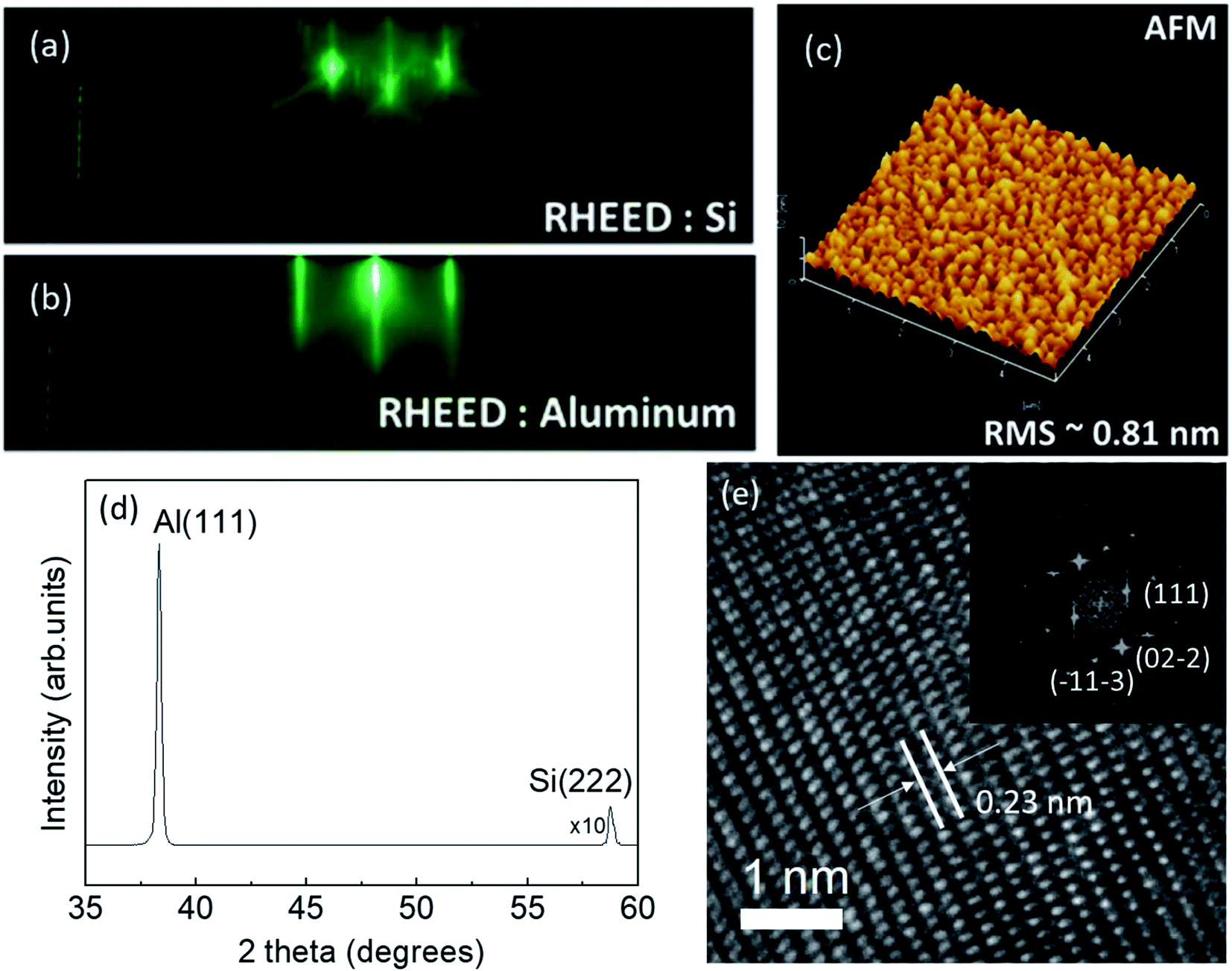 | ||
| Fig. 2 (a) RHEED patterns of well reconstructed Si (111) and (b) epitaxially grown Al film. (c) 5 × 5 μm2 top view atomic force microscope image of the single-crystalline Al film. The RMS roughness of the surface is about 0.81 nm. (d) XRD spectrum of the epitaxially grown Al film with a sharp Al (111) peak. (e) HRTEM image of the Al film with a lattice spacing of 0.23 nm, which corresponds to the interlayer spacing of the (111) planes in Al crystal lattice. Inset is the corresponding FFT pattern. | ||
The single ZnO nanowire with the length of 2.86 μm and the diameter of 120 nm on an Al film with about 3 nm-thick native oxide was pumped at 300 K with a pumping laser wavelength at 355 nm.28 Fig. 3a illustrates light-in light-out curve for the nanolaser. The spectra shown are measured for laser power between 1.42 MW cm−2 and 9.23 MW cm−2. From the light-light curve, we can obtain threshold for lasing to be about 6.39 MW cm−2 which is an extremely low threshold for a plasmonic laser. As the excitation power density is increased, several sharp peaks begin to emerge. In Fig. 3a, we can observe full width at half maximum (FWHM) is about 1.0 nm when lasing occured. Fig. 3b shows power-dependent emission spectra of the plasmonic laser, i.e. spontaneous emission (1.42 MW cm−2), amplified spontaneous emission (6.39 MW cm−2), and laser oscillation (7.81 MW cm−2 and 9.23 MW cm−2). There are sharp peaks appearing above the broad spontaneous emission background. In order to find the polarization distributions of the radiation intensity at the far field, a polarizer was placed in front of the spectrometer to measure polarization. From the polar plots of radiation intensity, we found that they were significantly polarized along the nanowire direction as shown in Fig. 3c. In addition, we also calculated its polarization ratio to be equal to 80%, shown in Fig. 3d.
 | ||
Fig. 3 The characteristics of a ZnO nanolaser. The ZnO nanowire is directly placed on Al film with native Al2O3. (a) The light-light curve and linewidth versus input power density at room temperature. (b) Measured spectra with the pumping power density from 1.42 MW cm−2 to 9.23 MW cm−2. (c) Polar plots of radiation intensity at the far field. The red solid spheres are the measurement results by placing a polarizer above the ZnO nanowire before the emission intensity is collected into fiber. (d) The polarization direction is parallel to the nanowire with a polarization degree of 80%. The polarization is defined as  where c is the nanowire axial direction. where c is the nanowire axial direction. | ||
To decrease the lasing threshold, inserting a dielectric layer to alleviate high optical loss caused by metallic regions is a feasible approach. Group velocity refractive index (group index) is a key parameter for evaluating the laser performance since larger group index means stronger interaction between plasmons and gain material. We estimate group index by the formula ng = (λ2/2ΔλL),29 where λ is the wavelength, Δλ is the longitudinal mode spacing, and L is the length of a nanowire. We then alter the thickness of Al2O3 to observe its variation in ability of optical confinement.
For comparison, we plot variation in threshold and group index with different thickness of Al2O3 of ten nanowires as seen in Fig. 4, showing the average threshold and group index values. Fig. 4a shows that average threshold values are 7.04 MW cm−2, 6.27 MW cm−2, 11.1 MW cm−2, and 18.2 MW cm−2 for the ZnO NWs on as grown Al (3 nm native oxide), 5 nm, 10 nm and 15 nm thick Al2O3/Al nanolasers, respectively. Fig. 4b shows average group index values calculated with the formula ng = (λ2/2ΔλL). We can find that ZnO nanowires dispersed directly on Al film possess the highest group index, while the lowest threshold was achieved for ZnO nanowires dispersed on ALD deposited 5 nm Al2O3 film on Al film.
 | ||
| Fig. 4 Threshold and group index comparison of the ZnO nanolaser. (a) Plot with error bar of threshold density. The average threshold values are 7.04 MW cm−2, 6.27 MW cm−2, 11.1 MW cm−2, and 18.2 MW cm−2 for the ZnO NWs on as-grown Al, 5 nm, 10 nm and 15 nm thick Al2O3/Al, respectively. The native oxide of Al film in all samples are 3 nm. (b) Plot of measured group index. | ||
Previous work shows that the surface roughness can be improved through ALD process.28 A confirmation can be obtained from AFM images shown in Fig. 5a and b depicting that the surface roughness of the native oxide is higher than ALD-grown Al2O3 The roughness of ALD-grown Al2O3 is 0.87 nm, which is considerably less than 1.14 nm of native oxide roughness, resulting in the lower optical loss on ALD-grown Al2O3. The native oxide was grown during the about 3 month period of exposure in air at made it rougher than the as-grown Al film shown in Fig. 2b. Fig. 5c shows the HAADF-STEM image and EDS analysis. From the EDS data, it can be seen that in ALD-grown Al2O3, the ratio of Al to O is close to 2:3, while there are much more oxygen vacancies existing in the native oxide. A close look at the ZnO/Al and ZnO/Al2O3/Al interfaces reveals that the quality of ALD deposited Al2O3 film is indeed superior to that of native oxide present at the ZnO/Al interface considering the surface roughness and microscopic defects.30 The results indicate that quality of aluminum oxide critically affects the lasing performance. Combining higher surface roughness on native oxide with more microscopic defects, the optical loss would be higher compared with Al2O3 grown by ALD. Hence, with 5 nm Al2O3 on Al film (in addition to 3 nm native oxide), ZnO nanolasers exhibit the lowest threshold due to the low metal loss. It is of interest that the refractive indices measured by ellipsometry are essentially the same, as shown in Fig. S1 in ESI.† The results indicate that the macroscopic parameters represented by refractive indices may not be the appropriate parameters for correlating with the thresholds of the lasing.
 | ||
| Fig. 5 Surface morphologies measured by AFM of (a) native Al2O3 and (b) ALD-grown Al2O3, the film roughness (RMS) is 1.14 nm and 0.84 nm, respectively. (c) High angle annular dark field scanning transmission electron microscopy (HAADF) image of 10 nm ALD-grown Al2O3 (II) on Al substrate with native oxide (I), and the EDS analysis of the two Al2O3 layer. | ||
The finite-difference time-domain (FDTD) solution is used to simulate the field energy density distribution of the ZnO nanowire laser lying on single-crystalline Al film with different thickness of Al2O3, as shown in Fig. 6. The simulated structure consists of a ZnO nanowire with hexagonal cross-section (side length = 60 nm) on different thickness of Al2O3 layer on Al film surface. Fig. 6 demonstrates that thinner dielectric layer will cause higher optical field confinement which does not reflect the relatively poor quality of native oxide compared with that of ALD-deposited Al2O3 layer. It points to the critical importance of the quality of dielectric layer, which has often been neglected in the theoretical calculation of electromagnetic field confinement. For further elaboration, we have also carried out the calculation with 3, 5, 10 and 15 nm-thick Al2O3 layer with simulated figures shown in Fig. S2 in ESI.† It shows that optical field confinement is the highest in samples with 5 nm-thick Al2O3 layer among all samples without taking consideration of the native oxide. It appears to be consistent with our experimental finding in the absence of sufficient understanding. Therefore, the present investigation reveals that neglecting the quality of the dielectric layer may lead to the misinterpretation of the data.
 | ||
| Fig. 6 Energy-density distribution of different thickness of Al2O3 in ZnO/Al2O3/Al structures with 3 nm native oxide calculated by FDTD. The excitation wavelength is 378 nm. White hexagons in the figures indicate the cross-section of ZnO nanowires. The side length of the ZnO nanowire is assumed to be 60 nm. | ||
In addition, the highest effective index, for material with restricted transverse extension such as nanowire, was calculated to occur in ZnO nanolaser with about 3 nm-thick native oxide as shown in the Fig. S3 in ESI,† which can be derived by the eigenmode method.16 The higher effective index is correlated to thinner dielectric layer, which means the distance between exciton and surface plasmon is shorter, and the energy transition rate between exciton and surface plasmon will be high enough to compensate the surface plasmon propagating loss. In addition, inserting optimal thickness of dielectric layer will alleviate high optical loss caused by metallic regions. However, when the dielectric layer is too thin, electron transfer will occur and lead to lower gain of active media.15,29 Coupled with the better quality of ALD-deposited Al2O3 layer, the best performance of our ZnO nanolasers can only be obtained with the optimal thickness of 5 nm ALD-deposited Al2O3 layer.
Summary and conclusions
Crystalline ZnO nanowires were dispersed on epitaxially MBE-grown Al film separated by a thin Al2O3 layer of various thickness deposited by ALD to form a Fabry–Perot type SPP cavities. We have successfully fabricated ultraviolet ZnO nanolasers that can operate at room temperature with low threshold due to large exciton binding energy of ZnO and high crystal quality for ZnO nanowires and aluminum film. The ZnO PL properties can be improved by annealing in Ar. For the system with 5 nm Al2O3 layer with 3 nm native oxide, a low threshold of 6.27 MW cm−2 for a plasmonic laser was obtained owing to the high optical gain and low metal loss. The optimal thickness of deposited dielectric layer leads to ultralow lasing threshold, which is 3 times and 12 times lower than that reported previously for ZnO/Al and Zno/Al2O3/Al plasmonic lasers. The quality of ALD-grown Al2O3 and native oxide are measured. Due to the defects and surface roughness, the nano laser with ALD-grown Al2O3 possesses better performance. The calculated energy-density distribution of the nanowire MOS structure by MED manifests the importance of the equality of Al2O3 dielectric layer. The results indicate that to lower the lasing threshold, both the thickness and quality of the dielectric layer should be taken into consideration. The present work represents a significant advance to the realization of room-temperature UV nanolasers with ultralow threshold by adjusting the thickness and quality of dielectric layer.Conflicts of interest
There are no conflicts to declare.Acknowledgements
The research was supported by the Ministry of Science and Technology through grants MOST 107-2221-E-007-055-MY3, MOST 107-3017-F-007-002, and MOST 105-2112-M-007-011-MY3.References
- S. Yokogawa, S. P. Burgos and H. A. Atwater, Nano Lett., 2012, 12(8), 4349–4354 CrossRef CAS PubMed.
- M. A. Guillorn, N. J. Loubet, C. W. Yeung, R. Chao, R. Muthinti, J. Demarest, R. Robison, X. Miao, J. Y. Zhang, T. Hook, P. Oldiges and T. Yamashita, 74th Annual Device Research Conference (DRC), 2016 Search PubMed.
- S. Gwo and C. K. Shih, Rep. Prog. Phys., 2016, 79(8), 086501 CrossRef PubMed.
- C. J. Lee, H. Yeh, F. Cheng, P. H. Su, T. H. Her, Y. C. Chen, C. Y. Wang, S. Gwo, S. R. Bank, C. K. Shih and W. H. Chang, ACS Photonics, 2017, 4(6), 1431–1439 CrossRef CAS.
- W. L. Barnes, A. Dereux and T. W. Ebbesen, Nature, 2003, 424(6950), 824–830 CrossRef CAS PubMed.
- S. A. Maier and H. A. Atwater, J. Appl. Phys., 2005, 98(1), 011101 CrossRef.
- M. Fox, Optical Properties of Solids, Oxford University Press, 2010, vol. 3 Search PubMed.
- R. F. Oulton, V. J. Sorger, D. A. Genov, D. F. P. Pile and X. Zhang, Nat. Photonics, 2008, 2(8), 496–500 CrossRef CAS.
- M. Castro-Lopez, D. Brinks, R. Sapienza and N. F. van Hulst, Nano Lett., 2011, 11(11), 4674–4678 CrossRef CAS PubMed.
- M. W. Knight, L. F. Liu, Y. M. Wang, L. Brown, S. Mukherjee, N. S. King, H. O. Everitt, P. Nordlander and N. J. Halas, Nano Lett., 2012, 12(11), 6000–6004 CrossRef CAS PubMed.
- M. W. Knight, N. S. King, L. F. Liu, H. O. Everitt, P. Nordlander and N. J. Halas, ACS Nano, 2014, 8(1), 834–840 CrossRef CAS PubMed.
- S. J. Tan, L. Zhang, D. Zhu, X. M. Goh, Y. M. Wang, K. Kumar, C. W. Qiu and J. K. W. Yang, Nano Lett., 2014, 14(7), 4023–4029 CrossRef CAS PubMed.
- S. Gwo, H. Y. Chen, M. H. Lin, L. Y. Sun and X. Q. Li, Chem. Soc. Rev., 2016, 45(20), 5672–5716 RSC.
- D. J. Bergman and M. I. Stockman, Phys. Rev. Lett., 2003, 90(2), 027402 CrossRef PubMed.
- Q. Zhang, G. Y. Li, X. F. Liu, F. Qian, Y. Li, T. C. Sum, C. M. Lieber and Q. H. Xiong, Nat. Commun., 2014, 2, 4953 CrossRef PubMed.
- Y. J. Lu, C. Y. Wang, J. Kim, H. Y. Chen, M. Y. Lu, Y. C. Chen, W. H. Chang, L. J. Chen, M. I. Stockman, C. K. Shih and S. Gwo, Nano Lett., 2014, 14(8), 4381–4388 CrossRef CAS PubMed.
- C. Y. Wang, H. Y. Chen, L. Y. Sun, W. L. Chen, Y. M. Chang, H. Ahn, X. Q. Li and S. Gwo, Nat. Commun., 2015, 6, 7734 CrossRef CAS PubMed.
- Z. Wang, J. Chen, Y. Mi, X. Sui, S. Zhang, W. Du, R. Wang, J. Shi, X. Wu, X. Qiu, Z. Qin, Q. Zhang and X. Liu, Adv. Opt. Mater., 2018, 6(22), 1800674 CrossRef.
- C. Huang, W. Sun, Y. Fan, Y. Wang, Y. Gao, N. Zhang, K. Wang, S. Liu, S. Wang, S. Xiao and Q. Song, ACS Nano, 2018, 12(4), 3865–3874 CrossRef CAS PubMed.
- M. H. Huang, S. Mao, H. Feick, H. Q. Yan, Y. Y. Wu, H. Kind, E. Weber, R. Russo and P. D. Yang, Science, 2001, 292(5523), 1897–1899 CrossRef CAS PubMed.
- Y. H. Chou, Y. M. Wu, K. B. Hong, B. T. Chou, J. H. Shih, Y. C. Chung, P. Y. Chen, T. R. Lin, C. C. Lin, S. D. Lin and T. C. Lu, Nano Lett., 2016, 16(5), 3179–3186 CrossRef CAS PubMed.
- Y. J. Lu, J. Kim, H. Y. Chen, C. H. Wu, N. Dabidian, C. E. Sanders, C. Y. Wang, M. Y. Lu, B. H. Li, X. G. Qiu, W. H. Chang, L. J. Chen, G. Shvets, C. K. Shih and S. Gwo, Science, 2012, 337(6093), 450–453 CrossRef CAS PubMed.
- F. Cheng, P. H. Su, J. H. Choi, S. Gwo, X. Q. Li and C. K. Shih, ACS Nano, 2016, 10(11), 9852–9860 CrossRef CAS PubMed.
- C.-W. Cheng, Y.-J. Liao, C.-Y. Liu, B.-H. Wu, S. S. Raja, C.-Y. Wang, X. Li, C.-K. Shih, L.-J. Chen and S. Gwo, ACS Photonics, 2018, 5(7), 2624–2630 CrossRef CAS.
- L. Zhou, C. Zhang, M. J. McClain, A. Manavacas, C. M. Krauter, S. Tian, F. Berg, H. O. Everitt, E. A. Carter, P. Nordlander and N. J. Halas, Nano Lett., 2016, 16(2), 1478–1484 CrossRef CAS PubMed.
- S. Tian, O. Neumann, M. J. McClain, X. Yang, L. N. Zhou, C. Zhang, P. Nordlander and N. J. Halas, Nano Lett., 2017, 17(8), 5071–5077 CrossRef CAS PubMed.
- Y.-C. Chang and L.-J. Chen, J. Phys. Chem. C, 2007, 111(3), 1268–1272 CrossRef CAS.
- J. Evertsson, F. Bertram, F. Zhang, L. Rullik, L. R. Merte, M. Shipilin, M. Soldemo, S. Ahmadi, N. Vinogradov, F. Carla, J. Weissenrieder, M. Gothelid, J. Pan, A. Mikkelsen, J. O. Nilsson and E. Lundgren, Appl. Surf. Sci., 2015, 349, 826–832 CrossRef CAS.
- R. F. Oulton, V. J. Sorger, T. Zentgraf, R. M. Ma, C. Gladden, L. Dai, G. Bartal and X. Zhang, Nature, 2009, 461(7264), 629–632 CrossRef CAS PubMed.
- A. Elloit, G. Malek, L. Wille, R. Lu, S. Han, J. Wu, J. Talvacchio and R. Lewis, IEEE Trans. Appl. Supercond., 2013, 23(3), 1101405 Search PubMed.
Footnotes |
| † Electronic supplementary information (ESI) available. See DOI: 10.1039/c9ra01484e |
| ‡ These authors contributed equally. |
| This journal is © The Royal Society of Chemistry 2019 |