
 Open Access Article
 This Open Access Article is licensed under a Creative Commons Attribution-Non Commercial 3.0 Unported Licence
Field-plate engineering for high breakdown voltage β-Ga2O3 nanolayer field-effect transistors†
Jinho Baea,
Hyoung Woo Kim b,
In Ho Kangb and
Jihyun Kim*a
b,
In Ho Kangb and
Jihyun Kim*a
aDepartment of Chemical and Biological Engineering, Korea University, Anamdong-5-Ga, Seoul 02841, South Korea. E-mail: hyunhyun7@korea.ac.kr
bKorea Electrotechnology Research Institute (KERI), Seongsan-gu, Changwon-si, Gyeongsangnam-do 51543, South Korea
First published on 27th March 2019
Abstract
The narrow voltage swing of a nanoelectronic device limits its implementations in electronic circuits. Nanolayer β-Ga2O3 has a superior breakdown field of approximately 8 MV cm−1, making it an ideal candidate for a next-generation power device nanomaterial. In this study, a field modulating plate was introduced into a β-Ga2O3 nano-field-effect transistor (nanoFET) to engineer the distribution of electric fields, wherein the off-state three-terminal breakdown voltage was reported to be 314 V. β-Ga2O3 flakes were separated from a single-crystal bulk substrate using a mechanical exfoliation method. The layout of the field modulating plate was optimized through a device simulation to effectively distribute the peak electric fields. The field-plated β-Ga2O3 nanoFETs exhibited n-type behaviors with a high output current saturation, exhibiting excellent switching characteristics with a threshold voltage of −3.8 V, a subthreshold swing of 101.3 mV dec−1, and an on/off ratio greater than 107. The β-Ga2O3 nanoFETs with a high breakdown voltage of over 300 V could pave a way for downsizing power electronic devices, enabling the economization of power systems.
Introduction
β-Ga2O3 is an attractive material for high-efficiency power devices owing to its ultra-wide energy bandgap (4.85 eV at room temperature), large breakdown field (approximately 8 MV cm−1), and excellent chemical and thermal stability.1,2 Its Baliga's figure of merit is estimated to be 3214.1 times greater than that of Si, which surpasses that of conventional wide-bandgap materials such as GaN (846.0) and 4H-SiC (317.1), suggesting its great potential as a near-future power device material.3,4 The commercial availability of a large single-crystal β-Ga2O3 substrate at its early R&D stage makes it more competitive compared to III-nitride semiconductors, which have suffered from the absence of a commercial freestanding substrate. Many techniques of growing an epitaxial β-Ga2O3 layer have been previously reported, including metal organic chemical vapor deposition and molecular beam epitaxy (MBE), and pulsed laser deposition.5–9 Thin film β-Ga2O3 power devices such as metal-oxide semiconductor field-effect transistors, Schottky diodes, and metal-semiconductor field-effect transistors (MESFETs) have demonstrated their potential as near-future, next-generation high-voltage electronic devices.10–15 Yang et al. fabricated edge-defined film-fed grown (EFG) Si-doped β-Ga2O3 thin-film vertical Schottky diodes with a reverse breakdown voltage of ∼2300 V.16 Wong et al. demonstrated MBE-grown Si-implanted thin-film β-Ga2O3 MOSFET with a breakdown voltage of 755 V.17Although β-Ga2O3 is not a van der Waals material, it can be easily separated into a single-crystalline nanolayer via mechanical exfoliation owing to its large anisotropy in the monoclinic lattice constants (a [100] = 12.225 Å, b [010] = 3.039 Å, and c [001] = 5.801 Å). Mechanically exfoliated β-Ga2O3 nanolayer flakes feature a strain-free and flat surface with a high crystallinity maintained. Hwang et al. reported a quasi-two-dimensional (quasi-2D) β-Ga2O3 layer obtained through the mechanical exfoliation of a β-Ga2O3 crystal, grown by the Czochralski method.18 Kim et al. demonstrated quasi-2D β-Ga2O3 MOSFETs with a stable operation at a high temperature of 250 °C, where the Ga2O3 was grown by the EFG method.19 Zhou et al. fabricated FET devices with an on/off current ratio of 1010 using Sn-doped β-Ga2O3 flakes.20 The exfoliated quasi-2D β-Ga2O3 nanolayers can be easily integrated with other 2D materials such as graphene, hexagonal boron nitride (h-BN), or transition metal dichalcogenides. The formation of a heterostructure by combining diverse nanolayers is intrinsically strain-free, i.e., the high crystal quality of each layer is maintained. The integration of n-Ga2O3 with a p-type 2D material, which is absent in β-Ga2O3, can enable a versatile device configuration that facilitates p–n heterojunctions and bandgap engineering.21–23 Kim et al. fabricated a 2D material-integrated β-Ga2O3 MOSFET by stacking h-BN on top of an exfoliated β-Ga2O3 nanolayer and analyzed the single- and dual-gate operations.24 A β-Ga2O3 quasi-2D MESFET with a stepped-gate structure was demonstrated by using 2D h-BN as a dielectric layer.25
The premature electrical breakdown induced by the concentrated electric fields limits the device operation under a high bias voltage and threatens the device reliability. Various techniques, such as a field-modulating plate, a stepped gate, and a recess gate structure, have been introduced to ease the peak electric field and enhance the breakdown voltage for high-power electronics.26–30 Among these, the field-modulating plate technique has been widely used owing to its efficacy and ease of fabrication. Studies have been conducted to increase the off-state electrical breakdown voltage using a gate or source field-plate, or multiple field-plates.31–33 However, such methods are rarely studied in nanodevices despite their potential in power nanoelectronics. The integration of a field-modulating plate with a β-Ga2O3 nanolayer can miniaturize the power circuit system and simplify the layout. In this study, we optimized the structure of a field-modulating plate on a β-Ga2O3 nanoFET through electric field simulations. Based on them, we fabricated high breakdown voltage quasi-2D β-Ga2O3 nanoFETs. The structural and electrical properties of the fabricated β-Ga2O3 nanoFETs with a field-modulating plate were systematically investigated.
Experimental details
A single crystalline β-Ga2O3 substrate (Tamura Corp.) with an effective carrier density of approximately 3.5 × 1017 cm−3, grown by the EFG method, was mechanically exfoliated into quasi-2D nanolayers using a commercial adhesive tape. The exfoliated β-Ga2O3 nanolayer flakes were transferred onto a thermally grown SiO2 (300 nm)/Si (500 μm) substrate via a standard dry transfer method. Both the source and drain electrodes were defined using an electron beam lithography (EBL) technique, followed by Ti/Au (50 nm/100 nm) metal deposition using an electron-beam evaporator. The optimal design of a field-modulating plate, in order to distribute the localized peak electric field of a β-Ga2O3 nanoFET device, was simulated using the device simulation software SILVACO Atlas. Rapid thermal annealing (Mila-5050, Ulvac Technologies, Inc.) under a low-vacuum condition (<10 mTorr) was performed at 500 °C for 1 min to improve the ohmic contact. The top-gate electrode of the β-Ga2O3 nanoFETs was deposited with Ni/Au (50 nm/100 nm), which was defined by the EBL and electron beam evaporation procedures. A SiO2 dielectric layer with a thickness of 200 nm was deposited using plasma-enhanced chemical vapor deposition (PECVD, VL-LA-PECVD, Unaxis), followed by the patterning of the field-modulating plate (Ti/Au (50 nm/100 nm)). The overall device fabrication process is shown in Fig. 1.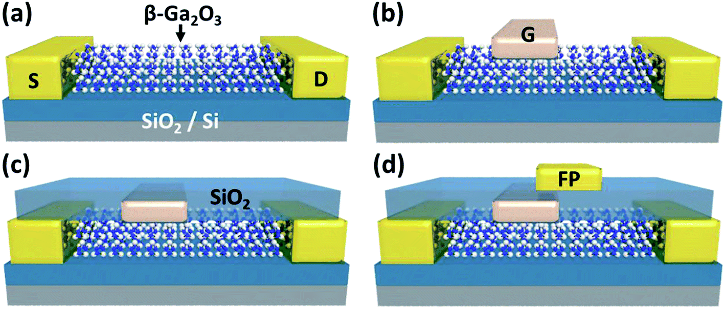 | ||
| Fig. 1 Fabrication process of a top-gated β-Ga2O3 nanoFET with a field-modulating plate. (a) Patterning of the source and drain ohmic contacts to the exfoliated β-Ga2O3 flake. (b) Deposition of the Ni/Au top gate electrode. (c) Deposition of the PECVD-SiO2 dielectric layer. (d) Patterning of the field-modulating plate (Ti/Au). | ||
The surface morphology and thickness of the fabricated field-plated FET devices were characterized using atomic force microscopy (AFM; Innova, Bruker). Micro-Raman spectroscopy was used to analyze the structural properties of the exfoliated β-Ga2O3 flakes under a back-scattering geometry using a 532 nm wavelength line of a diode-pumped solid-state laser (Omicron). The cross-sectional device structure and crystal orientation of the exfoliated β-Ga2O3 were investigated using scanning transmission electron microscopy (JEM-2100F, JEOL) after the specimen was prepared using the focused ion beam (FIB) technique (Quanta 3D FEG, FEI). The surface of the specimen was protected from FIB damage by a carbon layer. The electrical properties of the field-plated β-Ga2O3 MESFETs were monitored using an Agilent 4155C semiconductor parameter analyzer and 41501B single measurement unit expander connected to a probe station. The three-terminal off-state breakdown voltages of the fabricated β-Ga2O3 MESFETs were measured using a Keithley 6485 picoammeter connected with a Keithley 248 high-voltage supply. The fabricated β-Ga2O3 nanoFETs were immersed in a Fluorinert solution (FC-40, 3M) to prevent an unintended dielectric breakdown during the measurement of the three-terminal off-state breakdown voltage.
Results and discussion
Prior to the device fabrication, the optimal field-modulating structure that can effectively distribute the concentrated electric fields was investigated in order to prevent a premature breakdown and maximize the off-state breakdown voltage of the fabricated nanoFET devices. A schematic of the simulated device structure and LFP are presented in Fig. 2a. The simulations of electric field distribution were performed while varying the length of the field-modulating plate from the edge of the gate electrode to the source-grounded field-plate electrode (LFP). Using the numerical device analysis, the electric field distributions, which varied with the LFP under the conditions of VDS = +400 V and VGS = −50 V, are shown in Fig. 2b. The electric fields at the middle of the gate and drain electrodes were less than 3 MV cm−1, which is much lower than the breakdown field of β-Ga2O3 (∼8 MV cm−1). However, the electric fields were much higher at the drain edge of the gate (x = 0.5 μm) and the edge of the drain electrode (x = 2.5 μm). Generally, the peak electric field was observed at the drain-side edge of the gate electrode due to the bias condition of the FET. Once defective sites are created under the intense electric fields, they will grow and damage the device. These high-intensity, highly localized electric fields can eventually destroy it.34,35 Fig. 2b indicates the redistribution of the concentrated electric fields due to the presence of the field-modulating plate. In particular, at the drain-side edge of the gate electrode (x = 0.5 μm), the electric field was greatly alleviated by introducing the source-grounded field-plate structure, which is consistent with the previous reports of AlGaAs/GaAs, AlGaN/GaN, and SiC devices. In AlGaAs/GaAs HEMTs, the peak electric field was lowered by employing the field-modulating plate.36 Fig. 2c shows the maximum electric field values varying with LFP and proposes that the layout optimized for the dispersion of the concentrated electric fields is LFP ≅ 0.8 μm, which decreases the peak electric field from 11.4 MV cm−1 to 6.6 MV cm−1. The peak electric field (6.6 MV cm−1) redistributed by the source-grounded field-modulating plate was lower than the intrinsic breakdown field (∼8 MV cm−1) of β-Ga2O3, which can prevent a premature electrical breakdown during device operation and help to improve the device reliability. Fig. 2d and e compare the electric field distribution in β-Ga2O3 channel layer without and with a field-modulating plate, respectively. Fig. 2f shows the depth profile of the electric field in the β-Ga2O3 channel that varies with LFP. The electric field at the hot gate edge which is located in the drain-side gate edge was greatly mitigated by the introduction of field-modulating plate, enhancing the off-state breakdown voltage of the FET device. | ||
| Fig. 2 (a) Schematic of the β-Ga2O3 nanoFET with the field-modulating plate. (b) Simulation results of the electric field distribution between the gate and drain electrodes. (c) Maximum electric fields with varying field-plate lengths (LFP). Simulation results of the electric field distribution in β-Ga2O3 channel (d) without and (e) with the field-modulating plate of LFP ≅ 0.8 μm. (f) Depth profile of the electric fields calculated along the dotted line in the inset figure at varying LFP. | ||
Exfoliated β-Ga2O3 nanolayer MESFETs with a source-grounded field-plate were fabricated based on the optimized length of the field-modulating plate electrode (LFP = 0.8 μm). The optical microscopic image (Fig. 3a) and AFM image (Fig. 3b) confirm that the β-Ga2O3 nanoFETs were fabricated using the same layout as that suggested by the above electric field simulation. The β-Ga2O3 flakes used in this study had a thickness ranging from 200 to 350 nm with a root-mean-square roughness of approximately 1.3 nm (Fig. 3b), which is consistent with the result of the cross-sectional high-resolution TEM image (Fig. 3c). PECVD SiO2 conformally covered the Ni/Au top gate electrode. On top of the PECVD SiO2 layer, the Ti/Au field-plate electrodes were seamlessly defined with the optimized LFP (0.8 μm). A clear boundary was maintained between each layer without interdiffusion after the device fabrication process, as in Fig. 3c, which indicates the robustness of the exfoliated β-Ga2O3 nanolayer. The Raman spectrum of the fabricated nanoFETs is shown in Fig. 4a. No change in the Raman mode was observed after the device fabrication process, which also indicates the chemical and mechanical stability of the β-Ga2O3 nanolayer.37 The high crystallinity of the exfoliated β-Ga2O3 flake is also confirmed by the TEM image (Fig. 4b) and the selected area electron diffraction (SAED) pattern (Fig. 4c). The d-spacing in the SAED pattern was 0.609 nm, which matches the (200) lattice plane. This indicates that the mechanically exfoliated β-Ga2O3 flake was separated along the (100) direction due to the large anisotropy of the monoclinic β-Ga2O3 unit cell, even though β-Ga2O3 is not a van der Waals material.
 | ||
| Fig. 3 (a) Optical microscope image, (b) AFM image, and (c) cross-sectional high-resolution TEM image of the fabricated β-Ga2O3 nanoFET with the field-modulating plate. Note that a carbon layer was deposited to protect the specimen from FIB damage. | ||
 | ||
| Fig. 4 (a) Raman spectrum of the fabricated β-Ga2O3 nanoFET with the field-modulating plate. (b) Cross-sectional high-resolution TEM image and (c) SAED pattern of the mechanically exfoliated β-Ga2O3 flake. | ||
Eight β-Ga2O3 nanoFETs, each with a source-grounded field-plate, were fabricated. The electrical properties of the representative device are shown in Fig. 5. For comparison, the β-Ga2O3 nanoFET without the field plate was characterized, where the current density of the field-plated FETs was lower than that of the non-field-plated FETs because the voltage on the field plate competed with that on the gate electrode (Fig. S1†). They exhibited excellent DC output characteristics at varying VGS (Fig. 5a). The fabricated device showed n-type characteristics and was completely pinched off at a VGS of approximately −5 V. They showed a linear increase in the IDS under low-voltage operation below the knee voltage, and output currents were saturated above the knee voltage. Considering that conventional 2D material-based electronic devices suffer from the absence of output current saturation, the saturated output current in β-Ga2O3 nanoFETs show a potential for a nanoelectronic power amplifier. They also exhibited reproducible electrical characteristics without a significant change under the repeated driving conditions of VDS = +50 V. By contrast, 2D-material based electronic devices using graphene, black phosphorus, and transition metal dichalcogenides cannot withstand the high bias conditions used in our measurements of the fabricated β-Ga2O3 devices. Fig. 5b shows the transfer and transconductance characteristics of the fabricated β-Ga2O3 device. The field-effect mobility (μFE) was estimated to be 3.1 cm2 V−1 s−1, which was calculated by the following equation:

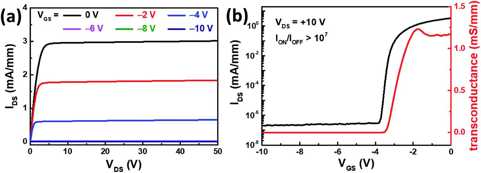 | ||
| Fig. 5 (a) DC output and (b) transfer/transconductance characteristics of the representative β-Ga2O3 nanoFET with the field-modulating plate at varying VGS. | ||
The three-terminal off-state hard-breakdown voltages of the β-Ga2O3 nanoFETs with and without a field-modulating plate are compared in Fig. 6a and b. The three-terminal off-state breakdown voltages were measured under the pinched-off condition. The devices under the test were immersed in Fluorinert solution to prevent unintentional dielectric breakdown due to ambient molecules, which is a standard test condition in power electronics. A high electric field can initiate carrier multiplication through impact ionization, where the accelerated carriers collide with the lattice and release their kinetic energy. The cascade creations of electron–hole pairs will result in high off-state currents, which will catastrophically damage the device. The impact ionization coefficients of β-Ga2O3 were estimated to be approximately 6.1 × 104 cm−1 and 9.5 × 103 cm−1 at the peak electric fields of 11.4 MV cm−1 (without field-modulating plate) and 6.6 MV cm−1 (with field-modulating plate), which are much lower than those of 4H-SiC (1.7 × 10⁶) and GaN (1.8 × 10⁴) at electric fields of 6.6 MV cm−1.38 The β-Ga2O3 shows a lower impact ionization coefficient under the same electric field due to its high bond strength of the binding energy of Ga–O (∼531 eV (O1s)), much larger than that of Ga–N (∼397 eV (N1s)) and Si–C (∼283 eV (C1s)). The breakdown field is generally proportional to (energy bandgap)2–2.5.2 This can reduce the off-state leakage currents and ensure a high hard-breakdown voltage. The hard-breakdown voltage of the field-plated β-Ga2O3 nanoFET was 314 V (Fig. 5b), while the hard-breakdown voltage of the β-Ga2O3 nanoFET without the field-modulating plate (Fig. 5a) was observed at VDS = 145 V. The two-fold increase of the hard-breakdown voltage is attributed to the existence of the field-modulating plate, which is consistent with the simulation results. The high off-state breakdown voltage of 314 V is much higher than those of conventional 2D devices (MoS2, 120 V) and wide-bandgap GaN nanowire device (140 V), opening a new route for next-generation high-power nanoelectronics with wide voltage swing.
 | ||
| Fig. 6 Off-state three-terminal hard-breakdown results of the fabricated β-Ga2O3 nanoFET (a) without and (b) with the source-connected field-modulating plate. The insets show the schematics of each device. | ||
Conclusion
A β-Ga2O3 nanoFET with an off-state hard-breakdown voltage of 314 V was fabricated by introducing a source-grounded field-modulating plate. The numerical device simulation was employed to analyze the effects of the field-modulating plate and determine the optimal structure to effectively distribute the electric fields concentrated on the hot gate edge. The β-Ga2O3 flakes, which were mechanically exfoliated from a single-crystal bulk substrate, was used as a n-channel layer with their crystallinity maintained. The fabricated nanoFET device showed excellent device characteristics including low SS and high on/off ratio with a high off-state hard-breakdown voltage (314 V). Engineering of the peak electric fields in a nanodevice by using a field-modulating plate improved the device stability under a high-voltage operation, paving the way for high-efficiency integrated power nanoelectronic systems.Conflicts of interest
There are no conflicts to declare.Acknowledgements
The research at Korea University was supported by the New & Renewable Energy Core Technology Program of Korea Institute of Energy Technology Evaluation and Planning (KETEP), which was granted financial resources from the Ministry of Trade, Industry & Energy, Korea (No. 20172010104830) and the Technology Development Program to Solve Climate Changes of the National Research Foundation (NRF) funded by the Ministry of Science and ICT (NRF-2017M1A2A2087351).References
- M. A. Mastro, A. Kuramata, J. Calkins, J. Kim, F. Ren and S. Pearton, ECS J. Solid State Sci. Technol., 2017, 6, P356 CrossRef CAS.
- S. Pearton, F. Ren, M. Tadjer and J. Kim, Appl. Phys. Rev., 2018, 124, 220901 CrossRef.
- B. J. Baliga, IEEE Electron Device Lett., 1989, 10, 455 Search PubMed.
- S. Pearton, J. Yang, P. H. Cary IV, F. Ren, J. Kim, M. J. Tadjer and M. A. Mastro, Appl. Phys. Rev., 2018, 5, 011301 Search PubMed.
- A. Kuramata, K. Koshi, S. Watanabe, Y. Yamaoka, T. Masui and S. Yamakoshi, Jpn. J. Appl. Phys., 2016, 55, 1202A1202 CrossRef.
- Y. Lv, J. Ma, W. Mi, C. Luan, Z. Zhu and H. Xiao, Vacuum, 2012, 86, 1850 CrossRef CAS.
- S. Rafique, L. Han, M. J. Tadjer, J. A. Freitas Jr, N. A. Mahadik and H. Zhao, Appl. Phys. Lett., 2016, 108, 182105 CrossRef.
- K. Sasaki, A. Kuramata, T. Masui, E. G. Víllora, K. Shimamura and S. Yamakoshi, Appl. Phys. Express, 2012, 5, 035502 CrossRef.
- F. Zhang, K. Saito, T. Tanaka, M. Nishio and Q. Guo, J. Cryst. Growth, 2014, 387, 96 CrossRef CAS.
- M. Higashiwaki, K. Sasaki, A. Kuramata, T. Masui and S. Yamakoshi, Appl. Phys. Lett., 2012, 100, 013504 CrossRef.
- M. Higashiwaki, K. Sasaki, T. Kamimura, M. Hoi Wong, D. Krishnamurthy, A. Kuramata, T. Masui and S. Yamakoshi, Appl. Phys. Lett., 2013, 103, 123511 CrossRef.
- M. J. Tadjer, N. A. Mahadik, V. D. Wheeler, E. R. Glaser, L. Ruppalt, A. D. Koehler, K. D. Hobart, C. R. Eddy Jr and F. J. Kub, ECS J. Solid State Sci. Technol., 2016, 5, P468 CrossRef CAS.
- S. Ahn, F. Ren, L. Yuan, S. Pearton and A. Kuramata, ECS J. Solid State Sci. Technol., 2017, 6, P68 CrossRef CAS.
- Z. Hu, K. Nomoto, W. Li, L. J. Zhang, J.-H. Shin, N. Tanen, T. Nakamura, D. Jena and H. G. Xing, Device Research Conference, 2017 Search PubMed.
- J. Yang, S. Ahn, F. Ren, R. Khanna, K. Bevlin, D. Geerpuram, S. Pearton and A. Kuramata, Appl. Phys. Lett., 2017, 110, 142101 CrossRef.
- J. Yang, F. Ren, M. Tadjer, S. Pearton and A. Kuramata, ECS J. Solid State Sci. Technol., 2018, 7, Q92 CrossRef CAS.
- M. H. Wong, K. Sasaki, A. Kuramata, S. Yamakoshi and M. Higashiwaki, IEEE Electron Device Lett., 2016, 37, 212 CAS.
- W. S. Hwang, A. Verma, H. Peelaers, V. Protasenko, S. Rouvimov, H. Xing, A. Seabaugh, W. Haensch, C. V. de Walle and Z. Galazka, Appl. Phys. Lett., 2014, 104, 203111 CrossRef.
- J. Kim, S. Oh, M. A. Mastro and J. Kim, Phys. Chem. Chem. Phys., 2016, 18, 15760 RSC.
- H. Zhou, M. Si, S. Alghamdi, G. Qiu, L. Yang and P. Ye, IEEE Electron Device Lett., 2017, 38, 103 CAS.
- J. Kim, M. A. Mastro, M. J. Tadjer and J. Kim, ACS Appl. Mater. Interfaces, 2018, 10, 29724 CrossRef CAS PubMed.
- G. Shin, H. Y. Kim and J. Kim, Korean J. Chem. Eng., 2018, 35, 574 CrossRef CAS.
- S. Nakagomi, T. Sakai, K. Kikuchi and Y. Kokubun, Phys. Status Solidi A, 2018, 1700796 Search PubMed.
- J. Kim, M. A. Mastro, M. J. Tadjer and J. Kim, ACS Appl. Mater. Interfaces, 2017, 9, 21322 CrossRef CAS PubMed.
- J. Bae, H. W. Kim, I. H. Kang, G. Yang and J. Kim, Appl. Phys. Lett., 2018, 112, 122102 CrossRef.
- Y. Ando, Y. Okamoto, H. Miyamoto, T. Nakayama, T. Inoue and M. Kuzuhara, IEEE Electron Device Lett., 2003, 24, 289 CAS.
- Y. Okamoto, Y. Ando, K. Hataya, T. Nakayama, H. Miyamoto, T. Inoue, M. Senda, K. Hirata, M. Kosaki and N. Shibata, IEEE Trans. Microwave Theory Tech., 2004, 52, 2536 CrossRef CAS.
- H. Xing, Y. Dora, A. Chini, S. Heikman, S. Keller and U. K. Mishra, IEEE Electron Device Lett., 2004, 25, 161 CrossRef CAS.
- C. Gaquiere, B. Bonte, D. Theron, Y. Crosnier, P. Arsene-Henri and T. Pacou, IEEE Trans. Electron Devices, 1995, 42, 209 CrossRef.
- T. Suemitsu, H. Yokoyama, T. Ishii, T. Enoki, G. Meneghesso and E. Zanoni, IEEE Trans. Electron Devices, 2002, 49, 1694 CrossRef CAS.
- R. Chu, A. Corrion, M. Chen, R. Li, D. Wong, D. Zehnder, B. Hughes and K. Boutros, IEEE Electron Device Lett., 2011, 32, 632 CAS.
- W. Saito, Y. Takada, M. Kuraguchi, K. Tsuda, I. Omura, T. Ogura and H. Ohashi, IEEE Trans. Electron Devices, 2003, 50, 2528 CrossRef CAS.
- J. Li, S. Cai, G. Pan, Y. Chen, C. Wen and K. Wang, Electron. Lett., 2001, 37, 196 CrossRef CAS.
- W. R. Frensley, IEEE Trans. Electron Devices, 1981, 28, 962 Search PubMed.
- B. J. Baliga, Semicond. Sci. Technol., 2013, 28, 074011 CrossRef.
- A. D. Rawal, S. Sharma, S. Kapoor, R. Liashram, R. K. Chaubey, S. Vinayak and R. K. Sharma, Def. Sci. J., 2018, 68, 290 CrossRef.
- C. Kranert, C. Sturm, R. Schmidt-Grund and M. Grundmann, Sci. Rep., 2016, 6, 35964 CrossRef CAS PubMed.
- K. Ghosh and U. Singisetti, J. Appl. Phys., 2018, 124, 085707 CrossRef.
Footnote |
| † Electronic supplementary information (ESI) available: DC output characteristics of the β-Ga2O3 nanoFETs with and without the field-modulating plate and the materials parameters for the device simulations. See DOI: 10.1039/c9ra01163c |
| This journal is © The Royal Society of Chemistry 2019 |