
 Open Access Article
 This Open Access Article is licensed under a Creative Commons Attribution-Non Commercial 3.0 Unported Licence
New functional material: spark plasma sintered Si/SiO2 nanoparticles – fabrication and properties
M. V. Dorokhin *a,
V. A. Gavvab,
M. V. Ved'a,
P. B. Deminaa,
Yu M. Kuznetsova,
I. V. Erofeevaa,
A. V. Nezhdanova,
M. S. Boldina,
E. A. Lantseva,
A. A. Popova,
V. N. Trushina,
O. V. Vikhrovaa,
A. V. Boryakova,
E. B. Yakimovc and
N. Yu. Tabachkovade
*a,
V. A. Gavvab,
M. V. Ved'a,
P. B. Deminaa,
Yu M. Kuznetsova,
I. V. Erofeevaa,
A. V. Nezhdanova,
M. S. Boldina,
E. A. Lantseva,
A. A. Popova,
V. N. Trushina,
O. V. Vikhrovaa,
A. V. Boryakova,
E. B. Yakimovc and
N. Yu. Tabachkovade
aLobachevsky State University of Nizhny Novgorod, 603950, Gagarin Ave. 23, Nizhny Novgorod, Russia. E-mail: dorokhin@nifti.unn.ru
bG. G. Devyatykh Institute of Chemistry of High-Purity Substances, Russian Academy of Sciences, 603951, Tropinina St. 49, Nizhny Novgorod, Russia
cInstitute of Microelectronics Technology and High-Purity Materials, Russian Academy of Sciences, 142432, Ac. Osipyan St. 6, Chernogolovka, Russia
dNational University of Science and Technology MISIS, 119049, Lenin Ave. 4, Moscow, Russia
eProkhorov General Physics Institute, Russian Academy of Sciences, 119991, 38 Vavilov Str., Moscow, Russia
First published on 29th May 2019
Abstract
A bulk nanostructured material based on oxidized silicon nanopowder was fabricated using a spark plasma sintering technique. Structural investigations revealed that this material has the composition of ∼14 nm core Si granules inside an SiO2 shell. Photoluminescence measurements have shown that the emission spectra lie in the energy range of 0.6–1.1 eV, which is not typical of the emissions of the Si/SiO2 nanostructures reported in numerous papers. This result can be explained by the formation of energy states in the bandgap and the participation of these states in both electronic transport and photoluminescence emission. Annealing of the sample leads to a decrease in defect density, which in turn leads to quenching of the 0.6–1.1 eV photoluminescence. In this case ∼1.13 eV inter-band transitions in the Si core start to play a dominant role in radiative recombination. Thus, the possibility of controlling the photoluminescence emission over a broad wavelength range was demonstrated.
Introduction
An ensemble of nanostructured silicon particles embedded into an SiO2 host has been the subject of intensive research over the last two decades.1–20 The main motivation for research in this field is the fabrication of silicon-based light emitters, which utilize the reduced dimension confinement effect to overcome indirect bandgap limitations for radiative recombination in Si.2,11,12,15 It is also worth citing some other applications of Si nanoparticles, such as photovoltaic cells,14,21,22 batteries,23,24 etc.Several methods for fabricating Si nanocrystals have been developed so far. In the early stages of investigations into the subject, ion implantation of Si+ into an SiO2 matrix followed by thermal annealing were used to fabricate Si nanocrystals in SiO2 films.1–3,7 Later, the method of SiO2/SiO or Si/SiO2 superlattice deposition and subsequent thermal annealing was developed. Electron beam evaporation or RF co-sputtering techniques were used to fabricate SiO2/SiO or Si/SiO2 heterostructures.3,5,6,8,10,13,16–18 Thermal annealing of SiOx layers fabricated by various chemical deposition techniques was also used.4,14,19 Considering Si nanoparticle powders, one could mention milling techniques and plasma torches; however, these methods are not often used for applications in optics.23–26 In the present paper, we report on the results of fabricating a bulk material consisting of Si nanoclusters in an SiO2 matrix. The material was fabricated by a spark plasma sintering (SPS) technique using oxidized silicon nanopowder. To the best of our knowledge, this is the first report on using the SPS method for the fabrication of Si/SiO2 luminescent nanostructures. This paper is focussed on an investigation of the structural properties, elemental composition and photoluminescence of the fabricated samples. The electrical characteristics of the bulk nanostructures were also studied.
A set of techniques, including Raman scattering, scanning electron microscopy equipped with an energy-dispersive X-ray spectroscopy (EDX) tool and X-ray diffraction (XRD) analysis, allowed us to show that the sintered samples represent an array of Si nanoclusters inside the silicon oxide shell. The samples possess a relatively high electrical resistance at room temperature and distinctive photoluminescence spectra with peaks in the energy range of <0.6 to ∼1.1 eV.
Usually the photoluminescence of Si/SiO2 nanoparticles is detected in the visible or/and near-infrared regions (above 1 eV) and is attributed either to the presence of defects in the oxide shell or to radiative recombination of excitons in the silicon crystal core.1–20 The origin of the 0.6 to ∼1.1 eV photoluminescence in the sintered structures is discussed, taking into account the undoubted recognition of the fabricated samples as Si nanostructures.
Sample preparation
The sample for investigation was fabricated by a two-stage process. The initial nanopowder was a by-product formed during the process of fabricating bulk polycrystalline silicon. Within this process, monosilane decomposition followed by deposition of silicon onto a heated (800 °C) rod-substrate were carried out in a wall-cooled reactor. In the latter type of reactor, a sharp radial temperature gradient is created (the gas temperature is a maximum near the surface of the rod and decreases sharply in the direction of the rod surface towards the walls of the reactor). Some of the monosilane molecules, when diffusing into the heated zone near the silicon rod, decompose in the gas phase into silicon and hydrogen, which is followed by Si atoms coalescing. Such Si complexes are pushed from the hot zone by the thermophoresis force and are deposited on the cold walls of the reactor. When removed from the reactor, the powder was exposed to air atmosphere; this caused an uncontrolled oxidation of the Si nanoparticles.At the next stage, the Si/SiOx core/shell powder was subjected to spark plasma sintering. A DR SINTER model SPS-625 spark plasma sintering system was used. The powder was placed into a graphite mold with an inner diameter of 12.8 mm and outer diameter of 30 mm and afterwards subjected to sintering at a constant heating rate (50 °C min−1). The heating was limited by a maximum temperature of 1020 °C, without any dwelling time. The mold + powder temperature was measured by a CHINO IR-AH pyrometer on the outer wall of the mold. At the end of the sintering process the sample was removed from mold and cut into plates with dimensions (length/width/height) 10 × 5 × 3 mm (the parts of the sample which were in contact with the mold were removed from consideration). Some plates were subjected to mechanical abrasion and polishing. In the final stage the sample surfaces were cleaned by treating with boiling toluene and (afterwards) acetone. The details of the spark plasma sintering method can be found elsewhere.27 Hydrostatic weighing of the fabricated sample showed that it was highly porous with a density of ∼0.46 of the density of bulk monocrystalline silicon.
In an attempt to decrease the size of the silicon core, the fabricated sample was subjected to oxidation by means of annealing in a dry high-purity oxygen atmosphere. The oxidation temperature was 850 °C and the time of oxidation was 240 s. Since the as-fabricated sample was highly porous, the oxygen penetration should be deep enough inside the sample. For that reason, we believe that the sintered particles were oxidized not only at the surface but deep inside the sample as well. This was confirmed by the measurement results to be presented below. Hereinafter this sample will be referred to as an oxidized one.
A transmission electron microcopy (TEM) image of the as-fabricated sample is shown in Fig. 1a. As can be seen from the figure, the sample consists of sintered near-spherical particles with an average size of ≈18 nm. One can also note the relatively large number of pores; the latter is in good agreement with the results of the hydrostatic weighing.
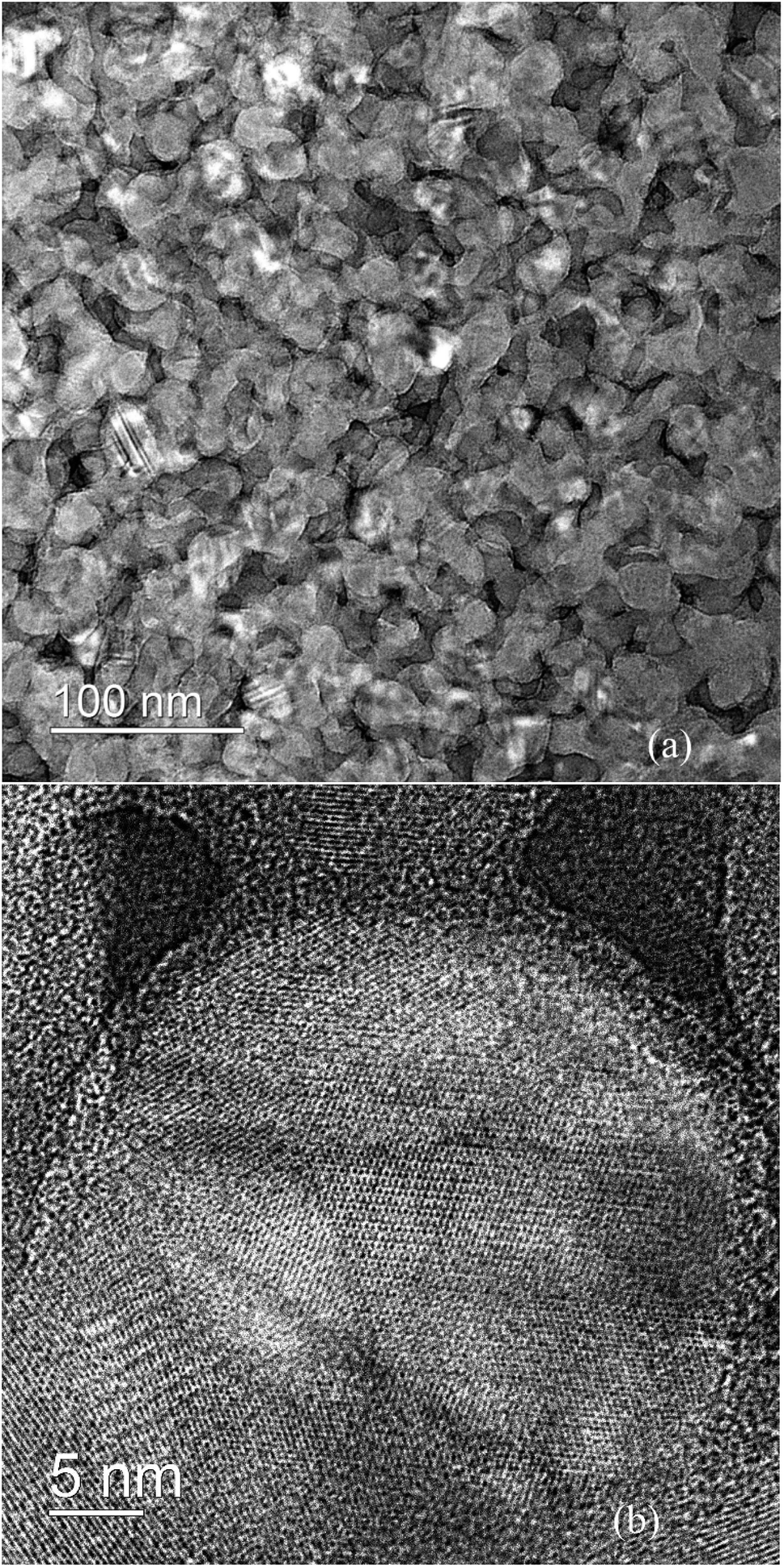 | ||
| Fig. 1 (a) An overview of the particle system of the sintered sample obtained by TEM; (b) high-resolution TEM image of a single particle in the sintered sample. Both images were converted to negative from the original TEM picture to emphasize the details. | ||
A closer look at the constituent particles has been made by obtaining the high-resolution TEM image of a single particle of the sample shown in Fig. 1b. The size of a particle shown in this figure is ∼20 nm. The particle represents a crystallographically ordered silicon core surrounded by an amorphous ∼2 nm shell which is attributed to SiO2. One can also see some defects in the atomic ordering of the Si core.
In addition, it is worth mentioning that a bridge connection between the particles can be seen at the top of Fig. 1b. The formation of such a bridge is typical during the process of nanoparticle sintering.27
Investigation details
The sample characterization started with an investigation of the crystalline structure and phase composition which was carried out using a Shimadzu 7000 X-ray diffractometer (Japan). CuKα radiation was used. Phase analysis of the sample was carried out on the basis of a DIFFRAC.EVA software complex, using a PDF-2 powder database. Based on the analysis, conclusions about crystallite size and phase composition were drawn.Another tool to investigate the chemical composition was an X-ray microanalysis EDX technique using an Oxford Instruments INCAx-sight energy dispersive system. The latter instrument was a part of a Jeol JSM-IT300LV scanning electron microscopy (SEM) instrument. An accelerating voltage was 20 kV and the probe current was less than 0.5 nanoampere. The measurements were carried out in high vacuum mode. The composition was calculated by the method of fundamental parameters implemented on the basis of the software of the microanalysis system.
The optical properties of the samples were investigated via photoluminescence and Raman spectroscopy. Raman spectroscopy was performed at room temperature using an NTEGRA Spectra AF + Confocal Raman system with a 473 nm wavelength laser and a spectral resolution of ≈0.5 cm−1. A laser beam was focused normally onto a surface by a 100× objective with a numerical aperture NA = 0.95. The laser spot diameter was ≈0.7 μm. The Raman signal was collected in backscattering mode.
Photoluminescence spectra were measured after illuminating the sample surface with a laser. Three different laser systems were used in order to avoid ambiguities in specification of the spectral lines. First, a semiconductor laser with a wavelength of 445 nm and a power varying within the range of 10–550 mW (445 nm laser) was used. The second one was a diode pumped solid state laser with a wavelength of 532 nm and power varying within the range of 0–300 mW (532 nm laser). Using two laser systems allowed the elimination of laser-related spectral lines. Finally, the presence/absence of PL emission in the range of 350–450 nm (2.75–3.5 eV) was checked using a pulsed nitrogen gas laser with a wavelength of 337 nm, pulse duration of 10 ns, repetition frequency of 50 Hz and a maximum power in the pulse up to 3 kW (337 nm laser).
The PL signal was analyzed by a calibrated grating monochromator system equipped with a cooled Hamamatsu G12181-110K InGaAs photodiode. The measurements were carried out at room temperature.
Finally, the temperature dependences of the resistivity of the cut plates of Si/SiOx core/shell nanostructures were measured. The measurements were performed within an automatic heating system with an independent sample temperature control using a thermocouple.
The resistance was measured between ohmic contacts alloyed onto the sample surface and recalculated into resistivity using the sample geometrical parameters. The material of the contacts was an Sb-based alloy.
Results and discussion
As has been discussed above, the sample is a disordered array of sintered nanoparticles, which are bridged with one another. The structure of the sintered material is well correlated with the parameters of the initial powder.The X-ray diffraction (XRD) investigations of the as-fabricated and oxidized samples give further information about the sample structure (Fig. 2). Both spectra represent the set of peaks corresponding to Si. The analysis of the recognized peaks width and position allowed calculation of the parameters of Si crystallites. The results are given in Table 1.
 | ||
| Fig. 2 XRD spectra of investigated samples: the as-fabricated sample is at the top, the oxidized sample is at the bottom of the picture. | ||
| a These data ignore ∼4 at% of C which is attributed to surface contamination. | ||
|---|---|---|
| Material | Si as-fabricated | Si oxidized |
| Crystallite size, nm | 13.5 ± 3.5 | 8.1 ± 1.5 |
| Cell parameter, Å | a = 5.43053 | a = 5.43088 |
| Concentration (EDX), at% | Si: 81.9 ± 1.0%; O: 18.1 ± 2.0% | Si: 50.5 ± 1.0%; O: 49.5 ± 2.0% |
The crystallite size calculated from the XRD spectra is lower than the average particle size visualized in the TEM image (Fig. 1a). The reasons for such disagreement are the presence of an amorphous SiO2 shell that does not make a contribution to the calculated size and defect complexes inside the silicon core that introduce some mistakes into the calculations.
A reliable SiO2-related signal was not revealed by the XRD measurements, which is obviously due to the amorphous state of the SiO2 shell as demonstrated in Fig. 1b. The presence of SiO2 was detected when measuring the surface of the sample subjected to mechanical polishing (not shown); however, no sign of SiO2 was detected in any of the measurements of unpolished surfaces. This fact does not allow us to attribute the XRD-detected SiO2 phase unambiguously either to the sample structure or to the polishing procedure.
The presence of an oxygen phase was detected by EDX measurements of the as-fabricated and oxidized samples. For the first one, composition measurements revealed about 18 at% of oxygen and 82 at% of silicon. Simple estimation shows that ∼9 at% of the 82 at% of silicon is oxidized. Then, considering the average particle size of 18 nm, one can estimate that the SiO2 shell is as thick as ∼2.5 nm, which is in good agreement with the EM measurements of the Si/SiO2 particle shown in Fig. 1a. We emphasize that, if we ignore carbon-related contamination, no sign of any elements other than Si and O was detected by EDX analysis.
For the oxidized sample, the oxygen content ratio was increased compared to the as-fabricated one. According to the EDX measurements (Table 1) the oxygen content was increased from ∼18 at% (for the as-fabricated sample) to ∼50 at% (for the oxidized one). The increase in oxygen ratio is obviously due to the oxidation of Si and the growth of the SiO2 shell. Such a process would consume silicon from the core, which should be followed by a decrease in core size. According to the EDX data (Table 1), approximately half of the entire silicon is oxidized. That allows us to recalculate the average size of the Si core to be ≈11 nm for the oxidized sample. This value is again lower than that estimated from the XRD data, which again can be explained by the inhomogeneities in the crystalline structure introducing some error into the determination of the crystallite size using XRD. However, the silicon core size decrease due to oxidation can be unambiguously seen from the XRD calculations.
Further material investigation was carried out using the Raman spectroscopy technique. The Raman spectra of the investigated samples and of a monocrystalline silicon plate are shown in Fig. 3. The dominant Raman shift peak for all samples is in the region of ∼520 cm−1 which is attributable to the Raman spectra for both monocrystalline and nanostructured silicon.28,29 Compared to the silicon plate, the Raman peaks of both the as-fabricated and the oxidized sample are broadened and shifted towards a higher wavelength.
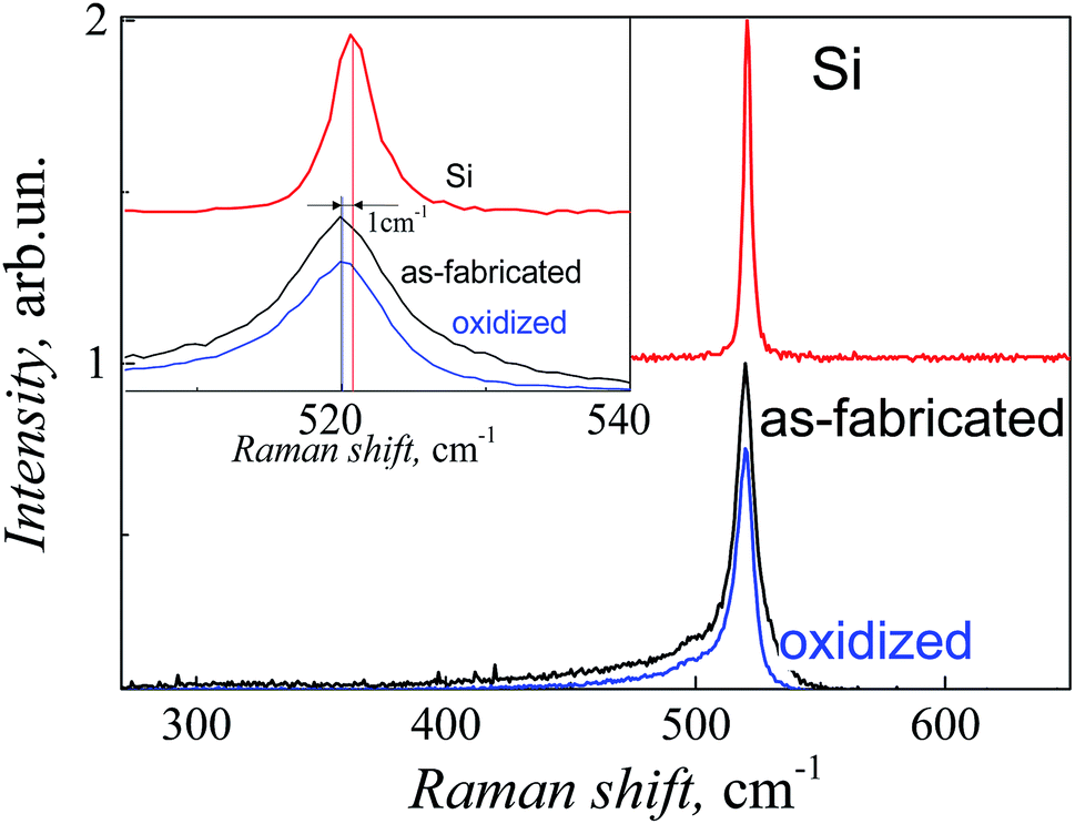 | ||
| Fig. 3 Raman spectra of investigated samples (as-fabricated and oxidized) and of a monocrystalline Si plate (Si) measured at 300 K. The inset shows the same spectra over a smaller wavelength range (510–540 cm−1). | ||
The difference between the maxima for Si and both as-fabricated and oxidized nano-Si is Δ ≈ 1 cm−1 (see inset to Fig. 3), which is characteristic of the crystallite size of the material. No measurable difference between the peak positions of both investigated samples can be seen from Fig. 4 (curves 2 and 3). Considering ref. 28 and 29, in which the Δ dependence on the crystallite size in nano-Si was studied, Δ ≈ 1 cm−1 corresponds to a crystallite size of 10–15 nm. For this range, the value of Δ depends very weakly on the crystallite size. Thus, the Raman shift difference between samples consisting of 10 nm or 15 nm crystallites should indeed be insignificant, as was obtained in Fig. 3. The range of 10–15 nm, although very broad, is in agreement with the crystallite parameters obtained by the TEM and XRD measurements.
 | ||
| Fig. 4 Photoluminescence spectra of the investigated nano-Si sample (as-fabricated) measured at 300 K irradiation by 445 nm 500 mW laser (1 blue and 2 black), 532 nm 300 mW laser (3 green), 445 nm 300 mW laser (4 blue) or 337 nm pulsed laser (5 violet). Curve 6 corresponds to measuring the oxidized sample by a 445 nm 400 mW laser. Curve 2 was measured 6 months after measuring curve 1. The spectra were recalculated to remove scattered laser radiation. The high-energy part of the spectrum was magnified. The inset shows the temperature dependence of the sample resistivity (dots) and (1) fitting function (line). | ||
The Raman peak full width at half maximum (FWHM) for the as-fabricated sample is ∼13.5 cm−1, which is much broader than that of monocrystalline Si. Such broadening is due to crystallite misorientation with respect to each other and the Si core size distribution of the sintered material. The sample annealing and oxidation lead to a decrease in the peak FWHM down to ∼8.5 cm−1. This is evidence for an improvement in the crystalline quality and homogeneity of the oxidized sample.
The photoluminescence spectra of the as-fabricated sample measured at room temperature are shown in Fig. 4. Unlike the majority of data on the PL spectra of nanostructured silicon, the emission in our case is detected only in the near-IR spectral range. One can see in Fig. 4 a set of broad peaks with an energy between 0.6 and ∼1.2 eV. It should be noted, however, that 0.6 eV is the border of InGaAs photodiode sensitivity, and thus the low-energy edge of the spectrum is unresolved.
Next, we emphasize that we have not detected any sign of PL emission different from that of the scattered laser radiation spectra in the visible light range (1.4–3.5 eV). The emission spectra in the 0.6 to ∼1.2 eV range differ strongly from scattered laser radiation and thus can only be associated with the sample itself. Increasing the laser power from 300 mW to 550 mW leads to an intensity redistribution between the PL lines (Fig. 4, curves 1 and 4), which can be associated with the charge carrier redistribution between the energy states involved in recombination. Such behaviour is typical for systems with two or more energy states in the bandgap (for example InAs/GaAs quantum dot heterostructures30).
Further validation of the revealed spectra was carried out by using two different laser systems (455 nm and 532 nm lasers) which have differing background spectra. In both cases the emission was detected over the same wavelength range (compare Fig. 4, curves 1–4). Moreover, one can note some similarity in spectra 1 and 2 obtained by 550 mW blue laser irradiation and 300 mW green laser irradiation, respectively. Considering the same pumping power of 300 mW for the 445 nm and 532 nm lasers (Fig. 4, curves 4 and 3, respectively) there is a difference between the spectral shapes and relative peak intensities. However, this difference is insignificant and can be associated with the different light penetration depths and absorption coefficients for green and blue lasers.
The final stage of the photoluminescence measurement of the sample was an investigation of stability. For this purpose, we have performed repeated measurements on the same sample. The second measurement was carried out immediately after the first one. The third measurement was carried out six months after the first two measurements at approximately the same place on the sample. The spectrum measured for the second time coincides with the first one, so that it has not been presented in the graph. The third spectrum of the same sample (after six-month storage) is shown in Fig. 4 (curve 2). This spectrum is again very similar to first one. Some insignificant differences in the spectral shape may be attributed to the different positions of the laser spot on the sample surface (there is a low probability of hitting exactly the same position on the sample). Thus, the sample optical properties are stable under both photoexcitation and six-month storage.
The annealing of the sample leads to modulation of the photoluminescence spectrum (Fig. 4, curve 6). First, the low-energy PL peaks at 0.6–0.8 eV were fully quenched in the annealed sample. On the whole, the emission signal of the annealed sample was detected in a narrower spectral band compared to the as-fabricated one and a smaller number of peaks can be resolved from the spectrum. The maximum of the PL intensity is shifted towards higher energy – to the position of ∼1.13 eV. In addition, the integral PL intensity was decreased by ∼5 times for the same laser excitation power. We should also emphasize that still no sign of the PL emission in the visible range of the spectrum was detected for the annealed sample.
Let us now discuss the origin of the photoluminescence of the samples. Numerous papers report on the emission of Si nanostructures in the wavelength range between 1.2 and 3.5 eV and even in the UV region.1–20 The exact positions of the peaks depend on the nanostructure parameters and fabrication technique. A maximum of three peaks were resolved in the PL spectra. Such a kind of emission is usually attributed to radiative transitions within the quantum-confined states in nanostructured silicon.
In the present study, the PL peaks are strongly redshifted compared with the reported ones, and a much greater number of peaks can be retrieved. Looking through papers studying the luminescence of silicon-based structures in the IR wavelength range, one can cite data on the deep-level photoluminescence of multicrystalline Si structures near an energy of ∼0.78 eV at 300 K. A broad 100 meV wide peak is attributed to energy states formed by a defect complex consisting of dislocation and oxygen impurity.31–33 Some papers on the luminescence associated with oxygen-related precipitates in silicon can be cited as well, but such luminescence is usually strongly quenched at 300 K.34,35 We believe that, in our case at least, the low-energy PL emission band can also be attributed to a set of defect complexes, which can be localized both inside Si nanocrystallites and on the Si/SiO2 interface. Within the PL emission process the photogenerated carriers thermalize on these defect states, which is followed by both radiative and non-radiative recombination with energies of <0.6 to 1.2 eV. At the same time, radiative recombination processes from both the inter-band and quantum-confined states are strongly suppressed due to the carriers escaping to the defect states. The possibility of dislocation and stacking fault formation in Si/SiO2 core/shell structures was experimentally demonstrated in ref. 36 and 37. We should also note that the conclusion in ref. 37 includes the prediction that defects should strongly influence the photoluminescence emission.
An unresolved issue is the origin of the defect-related broad band instead of a single 0.78 eV peak attributed to a dislocation complex in bulk multicrystalline silicon.31–33 To answer this question some additional measurement techniques are required. In the framework of the current paper, we confine ourselves to the hypothesis that such a difference may be caused by some other type of defects: for example stacking faults which were reported to be responsible for the photoluminescence in ref. 38.
The annealing of the sample leads to an improvement in the crystalline quality and supposedly decreases the defect density (as can be seen from the narrowing of the Raman peak in Fig. 3). Since the annealing temperature does not exceed the fabrication temperature, we believe that the improvement in quality is due to defect redistribution caused by both the annealing and decrease in particle size.37,38 For example in ref. 37 dislocation dissociation in Si nanocrystals was demonstrated as a result of annealing.
An improvement in crystalline quality should obviously be followed by a decrease in the density of states in the bandgap of silicon and quenching of the defect-related PL in the low-energy part of the spectrum, which is indeed observed in Fig. 4 (curve 6). Thus, the quenching of low-energy photoluminescence is another confirmation of its defect-related origin.
After the density of defect-related states in the Si bandgap has decreased, the carriers can no longer recombine within these states. In this case, the energy of the maximum PL intensity (∼1.13 eV) is very close to the bandgap of Si (1.12 eV at room temperature). We believe that the interband optical transitions in Si are responsible for such emission. This explains the low PL intensity of the annealed sample, since the radiative transition in silicon is indirect and is of very low probability. A small blueshift of the PL maximum with respect to bulk monocrystalline silicon can be associated with quantum size effects, as the bandgap increase in silicon nanostructures is an established fact.39–42 The small value of the shift (∼10 meV) is typical for the measured nanocrystallite size (Table 1).
Detailed investigation and modelling of the size dependence of the bandgap in Si nanostructures was carried out in ref. 39–42. The bandgap energy is most strongly influenced by nanoparticle arrays with a mean size below 4 nm. As for particles with a mean size over 8 nm (as in our samples) the bandgap energy very weakly depends on size and is very close to that of bulk silicon. This fact was confirmed by both experimental data and theoretical modelling for 1–10 nm nanoparticles.39–42
Thus, variation in particle size in the investigated sample by means of annealing did not lead to a significant nanostructuring effect, because the achieved nanoparticle mean size is not sufficiently small. However, we should emphasize significant changes in the PL spectrum, which are believed to be due to a complex effect of annealing and decreasing the particle mean size on decreasing the dislocation density. The spectrum of the annealed sample is similar to that obtained in ref. 6 (both as deposited and annealed at 1000 °C).
The electrical properties of the as-fabricated sample were investigated via measurements of the Seebeck voltage and temperature dependence of the resistivity. When measuring a Seebeck voltage, a temperature difference of ΔT was retained at the edges of the sample. The hot-edge potential was smaller than the cold-end potential, which corresponds to hole conductivity of the sample; thus holes are the majority carriers in the investigated sample. Such a situation is not typical for an undoped semiconductor sample. In particular, in samples with intrinsic conductivity the hot-edge potential is usually greater than that of the cold edge (due to higher mobility of electrons). Thus, one can suggest the presence of acceptor energy states in the sintered sample.
The temperature dependence of sample conductivity is presented in the inset to Fig. 4. At room temperature the sample is highly resistive, which is due to both the high purity of the initial materials and the probable spatial separation of Si nanoparticles by SiO2 barriers. With a temperature increase, the conductivity increases exponentially, which can be attributed to the semiconductor materials.
The σ(T) dependence presented in the inset to Fig. 4 can be approximated most accurately by a two-exponential fitting function:
σ ≈ A1![[thin space (1/6-em)]](https://www.rsc.org/images/entities/char_2009.gif) exp(E1/kT) + A2exp(E2/kT), exp(E1/kT) + A2exp(E2/kT),
| (1) |
We should emphasize that a detailed and more accurate conductivity analysis requires taking into account a set of mechanisms of electrical current: impurity band conductivity, hopping conductivity, tunnelling conductivity and the influence of contact resistance. This in turn would require a wider variation in the technological parameters, which is beyond the scope of this paper.
Within this paper both the values presented above and formula (1) are only rough estimates, illustrating the fact of an increase in exponential conductivity with an increase in the temperature.
Thus in the present study we have fabricated and investigated a new functional material based on an array of sintered Si/SiO2 core/shell nanoparticles. Such a material can be advantageous for applications in silicon-based optics because, compared with the analogous light-emitting structures based on Si, it has a much larger volume of emitting media. The overwhelming majority of silicon light-emitting nanostructures is based on thin-film technology.1–22,27–37 The thickness of the emitting region does not usually exceed tens of nanometers. The spark plasma sintering technique allows the fabrication of bulk nanostructured samples from which one would expect much higher luminescence intensity. No equivalent technical solutions for bulk nanostructures applicable in optics were found in the literature.
The as-fabricated samples demonstrate stable emission in the near-wavelength region, which cannot be achieved by other types of Si nanostructures (at least no data on this was found). Annealing of the sample and the subsequent decrease in nanoparticle mean size shifts the spectrum towards a lower wavelength, so that the emission properties become similar to those of the Si/SiO2 nanostructures studied in ref. 6. We believe that longer annealing at higher temperatures will lead to a further decrease in nanoparticle mean size and to a corresponding shift of the spectrum to the visible wavelength range. Thus, there is a potential capability of tuning the emission energy of the investigated structures from ∼0.6 eV to the visible range. This range includes part of the spectrum that has never been achieved by analogous Si nanostructures (at least at room temperature), which is another advantage of the investigated samples.
Finally, we should mention that such a material has multiple applications, not only in silicon-based optics, but also in electronics and as a thermoelectric material.43 The latter requires nanostructuring to decrease the thermal conductivity value, which would lead to an increase in efficiency.43
Conclusions
In conclusion, we have fabricated and investigated a new nanostructured material that consists of Si core nanoparticles in an SiO2 shell. The spark plasma sintering technique was used for the first time for sample fabrication. The photoluminescence investigation revealed a low-energy optical transition corresponding to the energy states in the gap of Si or SiO2. Hole conductivity of the material with a strong temperature dependence of resistivity were revealed. Annealing of the sample in an oxygen atmosphere led to the Si core size decreasing and to a decrease in the density of defects. This in turn led to the PL spectrum shifting towards a lower wavelength corresponding to the inter-band emission in ∼10 nm Si nanoparticles.Thus, the capabilities of the spark plasma sintering technique for the fabrication of semiconductor functional nanomaterials were demonstrated. The material demonstrates properties of both the bulk semiconductor and the nanoscale structure.
Conflicts of interest
There are no conflicts to declare.Acknowledgements
The part of work performed in Lobachevsky State University (Spark plasma sintering and sample characterization) was supported by the Russian Science Foundation (project # 17-79-20173). The part of the work performed by V. A. Gavva at the Institute of Chemistry of High-Purity Substances (Si/SiO2 powder fabrication) was supported within the framework of State Task No. 0095-2019-0008. The part of the work performed by E. B. Yakimov at the Institute of Microelectronics Technology and High-Purity Materials, Russian Academy of Sciences (chemical composition measurements) was financially supported within the framework of State Task No. 075-00475-19-00.References
- K. S. Zhuravlev, A. M. Gilinsky and A. Y. Kobitsky, Appl. Phys. Lett., 1998, 73, 2962, DOI:10.1063/1.122644.
- T. Shimizu-Iwayama, D. E. Hole and I. W. Boyd, J. Phys.: Condens. Matter, 1999, 11, 6595, DOI:10.1088/0953-8984/11/34/312.
- M. Zacharias, L. X. Yi, J. Heitmann, R. Scholz, M. Reiche and U. Gösele, Solid State Phenom., 2003, 94, 95, DOI:10.4028/www.scientific.net/SSP.94.95.
- T. P. Chen, Y. Liu, M. S. Tse, O. K. Tan, P. F. Ho, K. Y. Liu, D. Gui and A. L. K. Tan, Phys. Rev. B: Condens. Matter Mater. Phys., 2003, 68, 153301, DOI:10.1103/PhysRevB.68.153301.
- L. Pavesi, Z. Gaburro, L. Dal Negro, P. Bettotti, G. Vijaya Prakash, M. Cazzanelli and C. J. Oton, Opt. Laser. Eng., 2003, 39, 345, DOI:10.1016/S0143-8166(01)00140-3.
- X. X. Wang, J. G. Zhang, L. Ding, B. W. Cheng, W. K. Ge, J. Z. Yu and Q. M. Wang, Phys. Rev. B: Condens. Matter Mater. Phys., 2005, 72, 195313, DOI:10.1103/PhysRevB.72.195313.
- C. Gravalidis, S. Logothetidis, N. Hatziaras, A. Laskarakis, I. Tsiaoussis and N. Frangis, Appl. Surf. Sci., 2006, 253, 385, DOI:10.1016/j.apsusc.2006.06.019.
- Y. Liu, T. P. Chen, L. Ding, S. Zhang, Y. Q. Fu and S. Fung, J. Appl. Phys., 2006, 100, 096111, DOI:10.1063/1.2374929.
- I. Antonova, E. Neustroev, S. Smagulova and J. Jedrzejewski, Phys. Status Solidi C, 2009, 6, 2704, DOI:10.1002/pssc.200982586.
- K. Seino, F. Bechstedt and P. Kroll, Nanotechnology, 2009, 20, 135702, DOI:10.1088/0957-4484/20/13/135702.
- G. Seguini, S. Schamm-Chardon, P. Pellegrino and M. Perego, Appl. Phys. Lett., 2011, 99, 082107, DOI:10.1063/1.3629813.
- K. Seino, F. Bechstedt and P. Kroll, Mater. Sci. Eng., B, 2012, 177, 1098, DOI:10.1016/j.mseb.2012.05.016.
- K. Seino, F. Bechstedt and P. Kroll, Phys. Rev. B: Condens. Matter Mater. Phys., 2012, 86, 075312, DOI:10.1103/PhysRevB.86.075312.
- J. Huang, Y. Zeng, R. Tan, W. Wang, Y. Yang, N. Dai and W. Song, Appl. Surf. Sci., 2013, 270, 428, DOI:10.1016/j.apsusc.2013.01.042.
- T. Fangsuwannarak, K. Khunchana and S. T. Rattanachan, Key Eng. Mater., 2013, 545, 134, DOI:10.4028/www.scientific.net/KEM.545.134.
- T. Nikitin and L. Khriachtchev, Nanomaterials, 2015, 5, 614, DOI:10.3390/nano5020614.
- B. Han, Y. Shimizu, G. Seguini, E. Arduca, C. Castro, G. Ben Assayag, K. Inoue, Y. Nagai, S. Schamm-Chardond and M. Perego, RSC Adv., 2016, 6, 3617, 10.1039/c5ra26710b.
- E. M. L. D. de Jong, W. D. A. M. de Boer, I. N. Yassievich and T. Gregorkiewicz, Phys. Rev. B, 2017, 95, 195312, DOI:10.1103/PhysRevB.95.195312.
- Z.-L. Xu, X. Liu, Y. Luo, L. Zhou and J.-K. Kim, Prog. Mater. Sci., 2017, 90, 1, DOI:10.1016/j.pmatsci.2017.07.003.
- V. Bagratashvili, E. Feklichev, A. Rybaltovskiy, A. Sviridov, A. Shubnyy, S. Tsypina and A. Ischenko, J. Nanopart. Res., 2018, 20, 10P, DOI:10.1007/s11051-018-4138-1.
- S. Schafer, F. Haase, R. Peibst and R. Brendel, J. Appl. Phys., 2017, 122, 053102, DOI:10.1063/1.4997183.
- B. G. Gribov, K. V. Zinov'ev, O. N. Kalashnik, N. N. Gerasimenko, D. I. Smirnov, V. N. Sukhanov, N. N. Kononov and S. G. Dorofeev, Semiconductors, 2017, 51, 1675, DOI:10.1134/S1063782617130085.
- T. Matsumoto, K. Kimura, H. Nishihara, T. Kasukabe, T. Kyotani and H. Kobayashi, J. Alloys Compd., 2017, 720, 529, DOI:10.1016/j.jallcom.2017.05.228.
- J.-K. Ha, G. S. Chauhan, J.-H. Ahn, H.-J. Ahn and K.-K. Cho, Electrochim. Acta, 2016, 215, 674, DOI:10.1016/j.electacta.2016.08.114.
- V. I. Yusupov and V. N. Bagratashvili, Langmuir, 2018, 34, 12794, DOI:10.1021/acs.langmuir.8b01721.
- Y. Kobayashi, K. Imamura, T. Matsumoto and H. Kobayashi, J. Electr. Eng., 2017, 68, 17, DOI:10.1515/jee-2017–0050.
- V. N. Chuvil'deev, M. S. Boldin, A. V. Nokhrin and A. A. Popov, Acta Astronaut., 2017, 135, 192, DOI:10.1016/j.actaastro.2016.09.002.
- G. Viera, S. Huet and L. Boufendi, J. Appl. Phys., 2001, 90, 4175, DOI:10.1063/1.1398601.
- I. Iatsunskyia, G. Nowaczyk, S. Jurga, V. Fedorenko, M. Pavlenko and V. Smyntyna, Optik, 2015, 126, 1650, DOI:10.1016/j.ijleo.2015.05.088.
- N. N. Ledentsov, V. M. Ustinov, V. A. Shchukin, P. S. Kop'ev, Z. I. Alferov and D. Bimberg, Semiconductors, 1998, 32, 343, DOI:10.1134/1.1187396.
- M. Tajima, Y. Iwata, F. Okayama, H. Toyota, H. Onodera and T. Sekiguchi, J. Appl. Phys., 2012, 111, 113523, DOI:10.1063/1.4728194.
- M. Inoue, H. Sugimoto, M. Tajim, Y. Ohshita and A. Ogura, J. Mater. Sci.: Mater. Electron., 2008, 19, 132, DOI:10.1007/s10854-008-9605-5.
- H. T. Nguyen, M. A. Jensen, L. Li, C. Samundsett, H. C. Sio, B. Lai, T. Buonassisi and D. Macdonald, IEEE J. Photovoltaics, 2017, 7, 772, DOI:10.1109/JPHOTOV.2017.2684904.
- S. Binetti, S. Pizzini, E. Leoni, R. Somaschini, A. Castaldini and A. Cavallini, J. Appl. Phys., 2002, 92, 2437, DOI:10.1063/1.1497450.
- S. Pizzini, M. Acciarri, E. Leoni and A. Le Donne, Phys. Status Solidi B, 2000, 222, 141, DOI:10.1002/1521-3951(200011)222:1<141::AID-PSSB141>3.0.CO;2-H.
- Y. Q. Wang, T. Li, W. S. Liang, X. F. Duan and G. G. Ross, Nanotechnology, 2009, 20, 315704, DOI:10.1088/0957-4484/20/31/315704.
- Y. Q. Wang, W. S. Liang and G. G. Ross, ISRN Nanotechnol., 2011, 2011, 639714, DOI:10.5402/2011/639714.
- Y. Q. Wang, R. Smirani and G. G. Ross, Appl. Phys. Lett., 2005, 86, 221920, DOI:10.1063/1.1943501.
- M. Li, J. C. Li and Q. Jiang, Int. J. Mod. Phys. B, 2010, 24(15–16), 2297, DOI:10.1142/S0217979210064824.
- Y. Kanemitsu, H. Uto, Y. Masumoto, T. Matsumoto, T. Futagi and H. Mimura, Phys. Rev. B: Condens. Matter Mater. Phys., 1993, 48(4), 2827, DOI:10.1103/PhysRevB.48.2827.
- K. Takai, M. Ikeda, T. Yamasaki and C. Kaneta, J. Phys. Commun., 2017, 1, 045010, DOI:10.1088/2399-6528/aa8db4.
- B. Delley and E. F. Steigmeier, Appl. Phys. Lett., 1995, 67, 2370, DOI:10.1063/1.114348.
- G. Schierning, T. Claudio, R. Theissmann, N. Stein, N. Petermann, A. Becker, J. Denker, H. Wiggers, R. P. Hermann and R. Schmechel, Mater. Res. Soc. Symp. Proc., 2010, 1267, 1267-DD01-09, DOI:10.1557/PROC-1267-DD01-09.
| This journal is © The Royal Society of Chemistry 2019 |