DOI:
10.1039/C9RA01099H
(Paper)
RSC Adv., 2019,
9, 8039-8047
Structural, optical and photoelectric properties of Mn-doped ZnO films used for ultraviolet detectors
Received
12th February 2019
, Accepted 6th March 2019
First published on 11th March 2019
Abstract
Mn-doped ZnO (MZO) films were prepared on glass substrates using sol–gel dip-coating technology. The microstructural, morphological, optical and photoelectric properties of MZO films were investigated at different withdrawal speeds (WS: 20, 40, 60 and 80 mm s−1). The X-ray diffraction (XRD) patterns showed that all the films obtained were polycrystalline with a hexagonal structure, and the highest crystallinity of MZO films was observed as films were deposited at 40 mm s−1. The UV-Vis spectra revealed that the average optical transmittance of all samples was over 60% and the energy band gap of films decreased from 3.616 to 3.254 eV with the increase in withdrawal speed. The formed Au/MZO/Au photodetectors (PDs) indicate that a device prepared at 40 mm s−1 shows superior properties both in response speed and detection capability, and the rise time is 1.871 s and fall time is 3.309 s at 365 nm for 3 V bias and the detectivity (D*) reaches ∼1.7 × 10¹⁰ Jones. Moreover, the responsivity of PDs is also affected by the distance between Au electrodes and external bias. This research provides a simple way to fabricate the UV PDs based on MZO films with faster response and higher detectivity.
1. Introduction
Ultraviolet (UV) detectors are widely used in astronomy, combustion engineering, water purification, flame detection, biological effects and other fields.1–5 Over the years, wide band gap semiconductor materials (GaN, SiC and ZnO) have attracted more attention from researchers, especially for ZnO, due to its unique desirable properties such as wide band gap (3.2 eV), high exciton binding energy (60 meV), low cost, natural abundance and its ability to work in high temperature and damp environments.6–10 However, photoconductive UV detectors based on pure ZnO films show relatively poor response properties in the UV region, because of the large carrier concentration and fast recombination rate. Using dopants including Al, Ti, N, Li, Mg, Sn, Co and Mn to improve the performance of UV detectors have been widely discussed.11–15 In this paper, we chose Mn as the dopant in the ZnO films because of existence room temperature ferromagnetism in Mn-doped ZnO films and changing energy band gap.16 Furthermore, Ruan et al. has proved that behavior of doping Mn could increase the film resistivity, which contributes to decrease the dark current and improves the photosensitivity of UV detectors.17
There are many technologies to prepare ZnO films, such as chemical vapor deposition (CVD),18 physical vapor deposition (PVD),19 magnetron sputtering,20 hydrothermal method21 and spray pyrolysis.22 Although these processes are very mature, they also require high production conditions and cost which limit the further development of UV photodetectors based on ZnO films. Sol–gel dip-coating is a promising way to prepare uniform films with better adhesion between films and substrate through chemical bonds of –M–O–A–, where M and A are metallic ions in the films and substrate, respectively.23 Aydemir et al. suggested that the microstructural and optical properties of ZnO films using dip-coating are strongly dependent on the withdrawal speeds and also proved by other investigators.24,25 The systematic study of the fabrication UV photodetector based on Mn-doped ZnO (MZO) films at different withdrawal speeds has not been reported yet.
In this paper, we have successfully prepared Mn-doped ZnO (MZO) films on glass substrates by sol–gel dip-coating and the microstructural, morphological and optical properties of the MZO films were discussed by various ways. The results indicate that performance of films is strongly dependent on the film thickness controlled by the withdrawal speed. Moreover, the MZO films UV photodetector based on MSM structure were formed by sputtering Au electrodes on the film surface, and the response properties of devices were further investigated. This research aims to fabricate a Mn-doped ZnO UV photodetector (PDs) on glass substrates with a fast-response, rapid-recovery and that shows high sensitivity.
2. Experimental details
2.1 Sols preparation and deposition of Mn-doped ZnO films
Preparation process of Mn-doped ZnO (MZO) films is that zinc acetate dehydrate [(Zn(CH3CO2)2·2H2O), purity 99.5%] (Shanghai Aladdin Biochemical Technology Co., Ltd., China) dissolved in absolute ethanol (Chengdu Cologne Chemicals Co., Ltd., China) containing monoethanolamine (MEA) (Shanghai Aladdin Biochemical Technology Co., Ltd., China) that acted as a stabilizer. The mole ratio of MEA/zinc acetate dehydrate was kept at 1![[thin space (1/6-em)]](https://www.rsc.org/images/entities/char_2009.gif) :1 throughout the experiments. Also, the pH of solution was maintained at 9. The homogenous solution was then stirred at 45 °C for 0.5 h using magnetic stirrer to accelerate the hydrolysis reaction and then added Mn(NO3)2 solution (Chengdu Cologne Chemicals Co., Ltd., China) in the mixed solution and the Mn concentration was 2.5 at% with respect to Zn. After stirring for 2 h, the transparent sol was obtained and aged for 24 h. Mn-doped ZnO films were deposited on glass substrates (20 × 8 × 1 mm3) (Semerfly Technology Co., Ltd., China) using dip coating method and kept inside the bath for 30 s, then pulled upward at different withdrawal speed of 20, 40, 60 and 80 mm s−1, respectively. After coating each layer, the films were put in an oven at 90 °C for 5 min to evaporate the solvent existing in films. This process was repeated 10 times. Pure ZnO films were prepared using above method without adding Mn(NO3)2 solution. Finally, all samples were annealed in air at 500 °C for 2 h.
:1 throughout the experiments. Also, the pH of solution was maintained at 9. The homogenous solution was then stirred at 45 °C for 0.5 h using magnetic stirrer to accelerate the hydrolysis reaction and then added Mn(NO3)2 solution (Chengdu Cologne Chemicals Co., Ltd., China) in the mixed solution and the Mn concentration was 2.5 at% with respect to Zn. After stirring for 2 h, the transparent sol was obtained and aged for 24 h. Mn-doped ZnO films were deposited on glass substrates (20 × 8 × 1 mm3) (Semerfly Technology Co., Ltd., China) using dip coating method and kept inside the bath for 30 s, then pulled upward at different withdrawal speed of 20, 40, 60 and 80 mm s−1, respectively. After coating each layer, the films were put in an oven at 90 °C for 5 min to evaporate the solvent existing in films. This process was repeated 10 times. Pure ZnO films were prepared using above method without adding Mn(NO3)2 solution. Finally, all samples were annealed in air at 500 °C for 2 h.
2.2 Characterization of Mn-doped ZnO films
The structural properties of ZnO films were tested through X-ray diffraction (XRD) (SIEMENS D500) with Cu Kα radiation at a wavelength (λ) of 0.154 nm. Morphologies on the film surface were analyzed using the atomic force microscopy (AFM) (Asylum Research Cypher) and scanning electron microscope (SEM) (SIGMA 500) using an accelerating voltage of 20 kV. Optical performance of films were examined by UV-Vis (Shimadzu UV-2550) and Fourier transform infrared (FTIR) (Shimadzu IRPrestige-21) spectrophotometer. The gold (Au) electrodes were deposited on film surface by magnetron sputtering and the Mn-doped ZnO UV photodetectors were fabricated. The electrical characteristics of UV photodetectors were measured using a probe station with measuring instruments (Keithley 2400).
3. Results and discussion
3.1 Crystal structures of pure and Mn-doped ZnO films at different withdrawal speeds
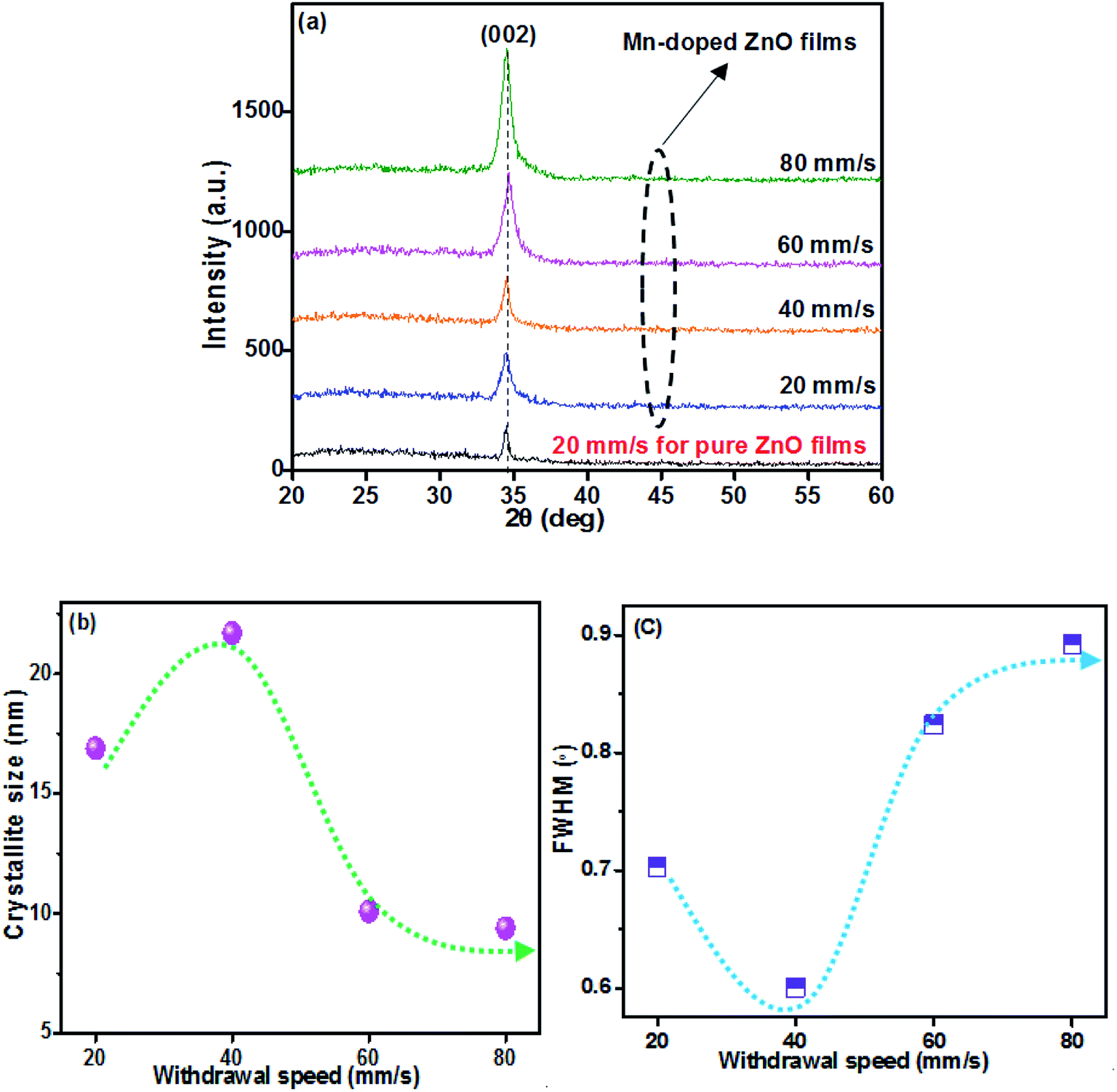
Film thickness is strongly affected by the withdrawal speed (WS), which is attributed to the competitive effects of gravitational and frictional viscous forces acting on the liquid film coating and solvent evaporation.26–28 The viscous drag of the moving substrate is proportional to the withdrawal speed and a larger force leads to a greater amount of the solution moving upwards with the substrates,29 so the film thickness increases with the increase of withdrawal speed. When the withdrawal speed increases from 20 to 80 mm s−1, the thickness of Mn-doped ZnO (MZO) films is 89, 134, 197 and 249 nm, respectively. Moreover, the thickness of 92 nm for pure ZnO films deposited at 20 mm s−1.
Fig. 1a shows the X-ray diffraction (XRD) patterns of MZO films deposited at different withdrawal speeds. The results indicate that only a diffraction peak at (0 0 2) plane can be observed, suggesting film growth along c-axis with hexagonal wurtzite structure belonging to P63mc space group and matching well with other works because of higher surface energy along {0 0 0 1} direction.13,30 The full-width at half-maximum (FWHM) of films decreases first and then increases with the increase of withdrawal speed, and the minimum of FWHM (0.6006) is obtained as the films prepared at 40 mm s−1, indicating highest order of crystallinity. The number of precursor solution is too small which is not conducive to the film growth as the withdrawal speed is the lowest, corresponding to 20 mm s−1. Continue to increase the withdrawal speed, the negative impact will be gradually weakened and the film thickness becomes thicker with larger crystallinity. However, if the withdrawal speed is over 40 mm s−1, it can be found, seen in Fig. 1b, that the crystallinity size of films abruptly decreases, because higher withdrawal speed means thicker film thickness and resulting in more difficult for the solvent to evaporate during heat treatment.31 Finally, the crystal growth will be blocked and a smaller crystallinity size in the films can be observed. These results indicate that the crystal growth of ZnO films is mainly determined by the film thickness which changes with the withdrawal speed. The changes in FWHM and crystallite size are shown in Fig. 1b and c. The crystallite size of MZO films is smaller than that of pure ZnO films prepared at the 20 mm s−1, due to the substitution of the relatively large ionic radius Mn2+ ions (0.080 nm) at the Zn2+ (0.074 nm) sites, resulting in expanding the lattice parameters and damage the film growth.
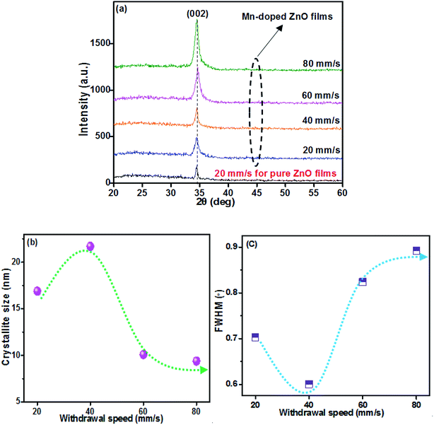 |
| | Fig. 1 X-ray diffraction (XRD) analysis of Mn-doped ZnO films prepared at different withdrawal speeds. (a) XRD patterns, (b) crystallite size, (c) the full-width at half-maximum (FWHM). | |
3.2 Surface morphologies of MZO films prepared at various withdrawal speeds
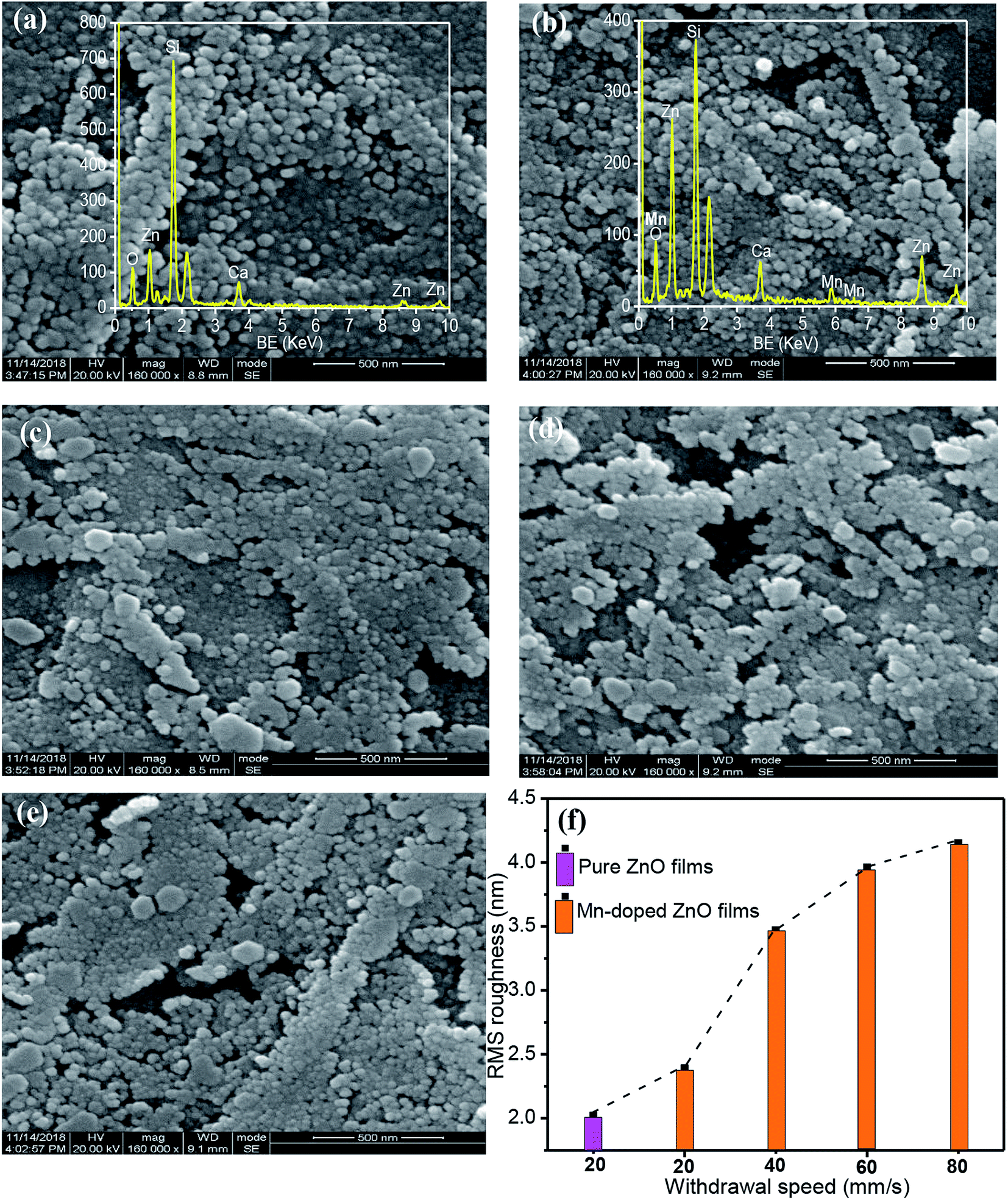
Fig. 2 displays the surface morphologies of pure and Mn-doped ZnO (MZO) films using SEM. As the withdrawal speed is lowest, corresponding to 20 mm s−1, the formed films is thinnest and the solvent existing in films will be more evaporated during heat treatment. This behavior can make a large shrinkage for film surface and obtain the compact layers,31 as shown in Fig. 2a and b. Meanwhile, grains on the film surface show granular shape with uniform distribution, due to lower film thickness. Energy dispersive spectrometer (EDS) result proves that presence of Zn, O, Si and Ca elements in the pure ZnO films deposited as 20 mm s−1 while Mn species can be observed in Mn-doped ZnO films besides above mention elements, just as seen in insets of Fig. 2a and b. With the increase of film thickness changing with withdrawal speed from 20 to 40 mm s−1, MZO films become denser and part of grains with granular shape change into hexagonal structure. But if the withdrawal speed is over 40 mm s−1 and up to 80 mm s−1, there are some pores can be noticed among grains and film surface becomes rougher, suggesting a deterioration of the crystal quality. The formed pores may be attributed to the grain agglomeration which is related to the higher thickness.24 Additionally, the root mean square (RMS) roughness of films, shown in Fig. 2f, is affected by the withdrawal speed which determines the film thickness. Mn-doped ZnO films deposited at 20 mm s−1 show a larger RMS roughness related to the pure ZnO films and as the withdrawal speed increases from 20 mm s−1 to 80 mm s−1, the value of RMS roughness of MZO films gradually enhances, which is attributed to the increase in film thickness and confirmed by other reports.24,32
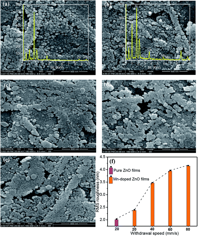 |
| | Fig. 2 Surface morphologies of pure and Mn-doped ZnO films deposited at different withdrawal speeds. (a) 20 mm s−1 for pure ZnO, (b) 20 mm s−1, (c) 40 mm s−1, (d) 60 mm s−1, (e) 80 mm s−1, (f) RMS roughness of films. | |
3.3 Transmittance spectra and FTIR spectra of Mn-doped ZnO films
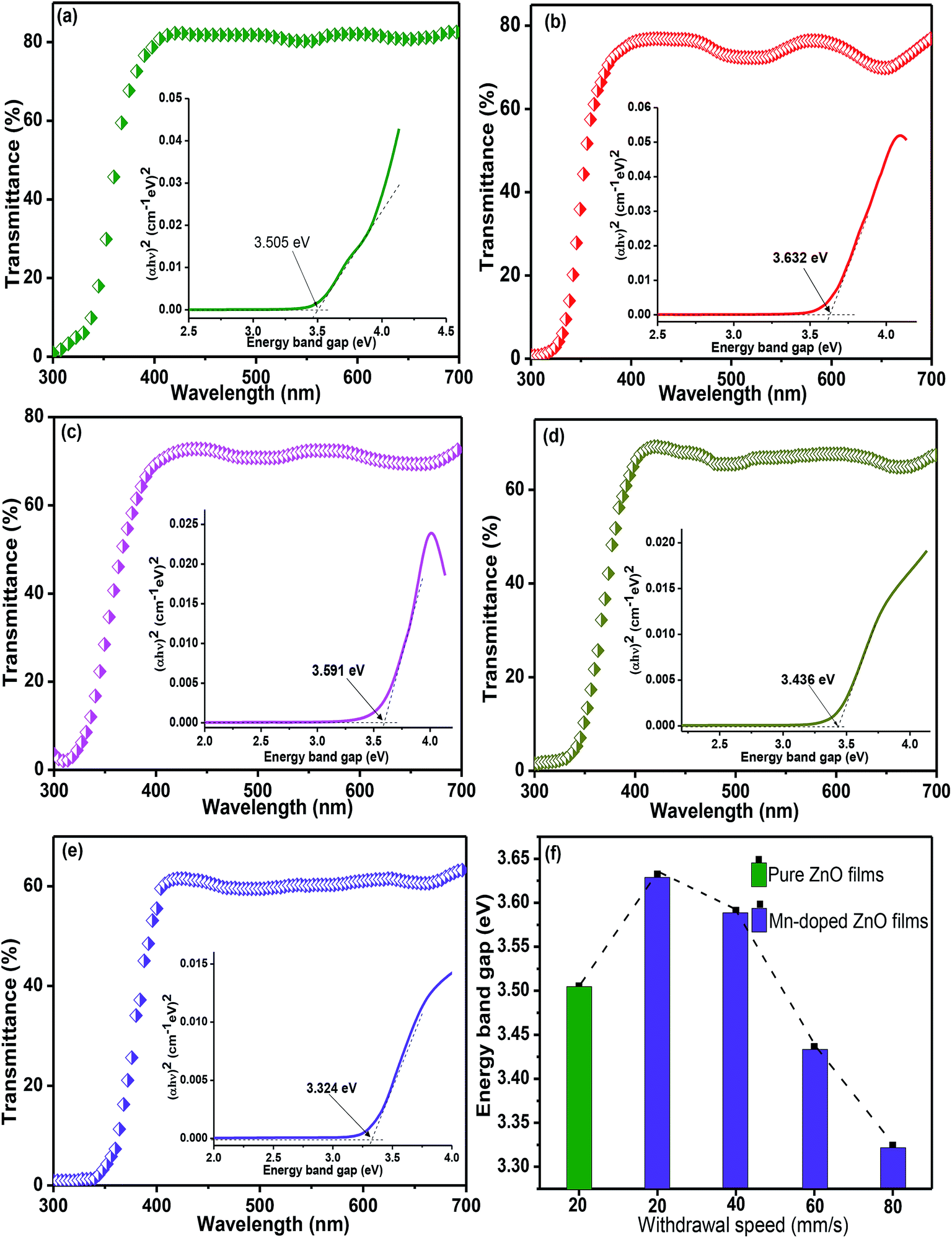
Fig. 3a–e presents the transmittance spectra of pure and Mn-doped ZnO (MZO) films as recorded in the range from 300 to 700 nm. All samples exhibit a high transmittance of over 60% in the visible regions, but a sharp drop is observed below 400 nm, which is related to the intrinsic band-gap of films.33 It is clearly found that compared to pure ZnO films, Mn-doped ZnO films prepared at 20 mm s−1 show a lower transmittance which is related to the oxygen vacancies and scattering at grain boundaries.34 Also, for MZO films, the average transmittance in the visible range gradually declines as the withdrawal speed increases from 20 mm s−1 to 80 mm s−1. Noticeable, increase in withdrawal speed means increasing film thickness and larger thickness exhibits a lower transmittance, a similar result was also reported from Rajalakshmi et al.35 Moreover, the relationship between energy band gap (Eg) and withdrawal speed is shown in Fig. 3f and indicating that increase in withdrawal speed will decrease the Eg for Mn-doped ZnO films, due to the increase in film thickness. Some people have proved that the Eg of films is found to decline as the film thickness increases, this is due to the existence some film stress and defects in the films with larger thickness, and then decrease in Eg.36,37 The energy band gap of MZO films is larger than that for pure ZnO films, due to the sp–d spin exchange interaction.34
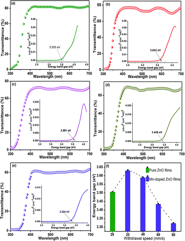 |
| | Fig. 3 Optical transmittance spectra of Mn doped ZnO films prepared at various withdrawal speeds. (a) 20 mm s−1 for pure ZnO, (b) 20 mm s−1, (c) 40 mm s−1, (d) 60 mm s−1, (e) 80 mm s−1, (f) energy band gap of films. | |
Generally, the Fourier transform infrared (FTIR) spectra provides information about functional groups and chemical bonding present in the materials.16 Fig. 4 shows the FTIR spectra of pure and MZO films prepared at 20 mm s−1. For pure ZnO films, the absorption peak at 500 cm−1 is attributed to Zn–O stretching mode. The peak at about 2340 and 3400 cm−1 is due to CO2 molecules and –OH group, respectively, suggesting the existence air including water absorbed on the film surface. The peak around 2896 cm−1 is observed and related to the C–H bond bending mode.38,39 Compared to Fig. 4a, a new peak at 680 cm−1 is observed in Fig. 4b and assigned to Mn–O vibration mode. The shift towards higher wavenumber for Mn-doped ZnO films is observed, which is attributed to the substitution of Mn ions at Zn site in the crystal lattice.40
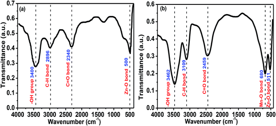 |
| | Fig. 4 FTIR spectra of films prepared at 20 mm s−1. (a) Pure ZnO films, (b) Mn-doped ZnO films. | |
3.4 The performance of UV photodetectors based on pure and Mn-doped ZnO films
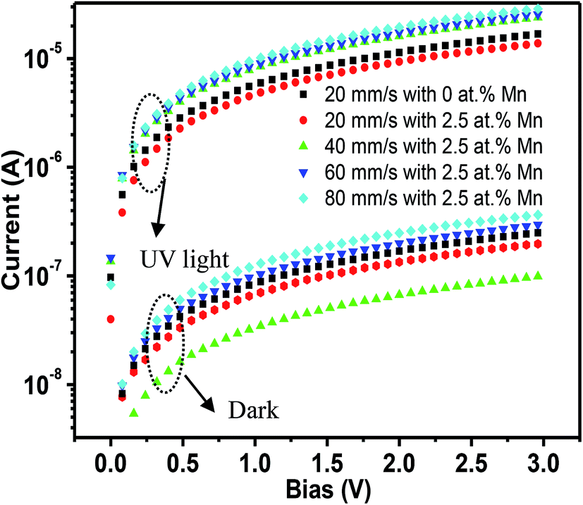
I–V characteristics under dark and UV light conditions for MZO films deposited at different withdrawal speeds in log-scale are shown in Fig. 5. The wavelength and power density of incident light are 365 nm and 10 mW cm−2, respectively. Also, the area of film surface exposed to light is 0.8 cm2. When the PDs are exposed to UV light, the current, regards as the photocurrent, abruptly increases and much higher than one in dark, due to the discharge of the oxygen ions and decrease in depletion width on the film surface. ZnO films exhibit higher values in the photocurrent and dark current, compared to MZO films prepared at 20 mm s−1. The substitutional Mn at Zn sites in ZnO crystal lattice, confirmed by EDS and FTIR analysis, will increase the film resistivity, resulting in lower dark current. Meanwhile, the formation of dark current is related to the defects such as oxygen vacancies and/or Zn interstitials and Hlaing Oo et al. reported that the conductivity of ZnO films prepared by metalorganic chemical vapor deposition (MOCVD) decreases with increasing Mn content, which is attributed to the substitutional Mn at Zn sites can effectively suppress the produce of native defects including oxygen vacancies.41 For MZO films, with the withdrawal speed increases from 20 mm s−1 to 80 mm s−1, the photocurrent of devices gradually improves, due to the smallest energy band gap and existence obvious defects in the films with largest thickness.
 |
| | Fig. 5 I–V characteristics of pure and Mn-doped ZnO films deposited at different withdrawal speeds. | |
Fig. 6a–d shows the switchable photocurrent response to 365 nm excitation at 10 mW cm−2 using 3 V bias. The rise time (τr) and fall time (τf) are defined as the time taken by the photodetector to increase its maximum photocurrent from 10% (90%) to 90% (10%) of the peak value.15 Usually, the charge carriers will take more time to relax and τf is found to be larger than τr, because of existence deep trap states and other defects in films.42 The results exhibit MZO films prepared at 20 mm s−1 in comparison to ZnO films show faster response with the τr of 4.087 s and τf of 5.462 s. The formation of MnO (3.6 eV) or MnO2 (0.25 eV) caused by the substitutional Mn at Zn sites can produce the heterojunction in the interface of ZnO/manganese oxide and promote the electronics transfer to Au electrodes.43 Therefore, Mn-doped ZnO films at 20 mm s−1 show faster response in comparison to pure films. For Mn-doped ZnO films, the response properties of PDs are strongly affected by the withdrawal speed and with the withdrawal speed increases from 20 mm s−1 to 80 mm s−1, the response time and recovery time of devices decrease at first and then increase and films deposited at 40 mm s−1 represent the fastest speed with the τr of 1.871 s and τf of 3.309 s, suggesting highly efficient photosensitive switch. The results can be analyzed by following mechanisms. As we known that the response time of PDs is mainly determined by the electronic migration capacity in the films. Electrons can travel quickly through large grains, due to lower grain boundaries density in the films containing bigger grains. Meanwhile, majority of defects can be existed in grain boundaries which will trap the electrons and suppress the migration, resulting in longer response time. The value of fall time of PDs is related to the recombination rate between electron–hole pairs, which is controlled by film crystallinity. In previous report, our group has proved that higher crystal quality in the ZnO films prepared by sol–gel method can accelerate the recombination process, because of decrease in trap center formed by defects.44 Therefore, Mn-doped ZnO films deposited at 40 mm s−1 show the fastest response speed and recovery speed while a poor response properties for films deposited at 80 mm s−1, due to the poor crystal quality and the number of grain boundaries, which is associated with the film thickness.
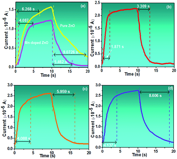 |
| | Fig. 6 Response and recovery-current characteristics of pure and MZO films PDs deposited at various withdrawal speeds. (a) 20 mm s−1, (b) 40 mm s−1, (c) 60 mm s−1, (d) 80 mm s−1. | |
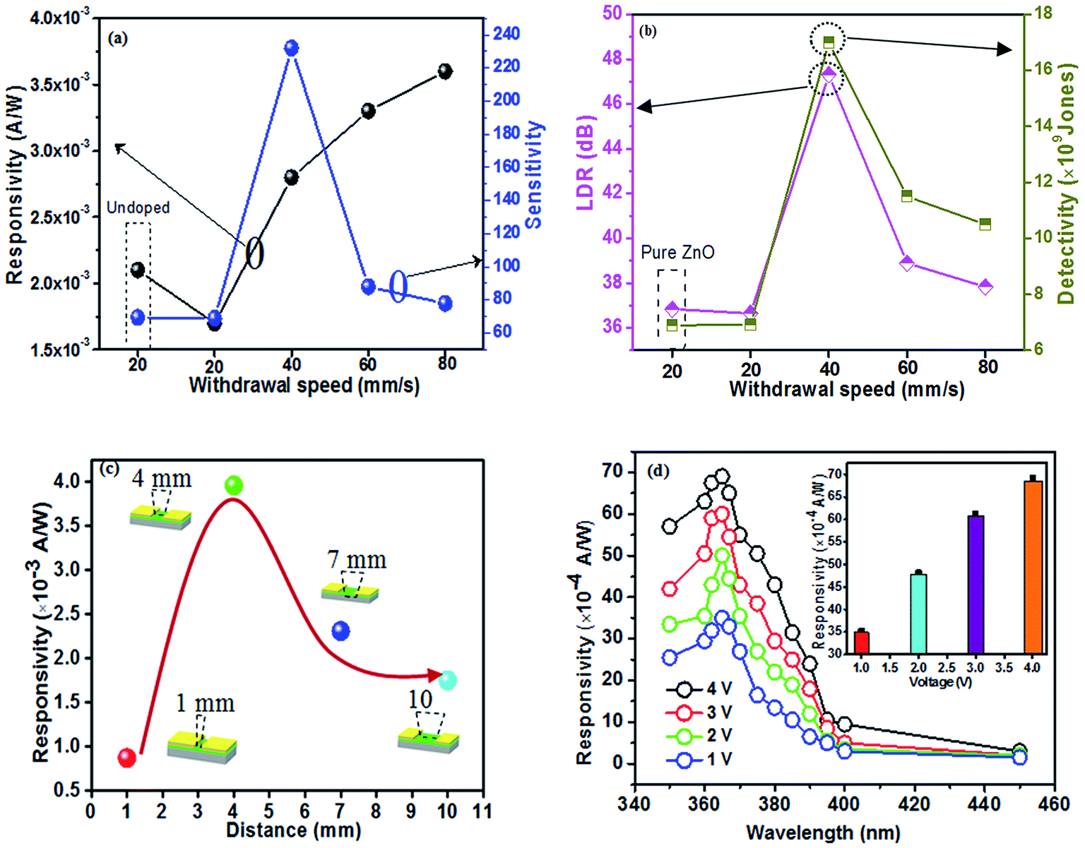
In addition to the response and recovery time, parameters including responsivity (R) and sensitivity (S) are also vital to evaluate the performance of UV PDs. The responsivity and sensitivity of devices can be calculated using following equation.45
| |
 | (1) |
| |
 | (2) |
where,
Iph,
Idark, and
Pop are the values of the photocurrent, dark current, and optical power of UV light, respectively. The values of them are shown in
Fig. 7a. It can be found, for MZO films UV PDs, with the withdrawal speed increases from 20 mm s
−1 to 80 mm s
−1, the responsivity of PDs gradually improves and films prepared at 80 mm s
−1 show the highest responsivity of 3.6 × 10
−3 A W
−1, which is related to the largest photocurrent. Moreover, films deposited at 40 mm s
−1 exhibit biggest sensitivity to the UV light (
λ = 365 nm, 10 mW cm
−2) at the bias of 3 V. Furthermore, PDs based on ZnO films exhibit a higher sensitivity than that for MZO films at 20 mm s
−1, due to the smaller energy band gap and higher conductivity. Linear Dynamic Range (LDR) is used as a way to judge the accuracy of results measured by the devices and the values of LDR were calculated by following equation.
14| |
 | (3) |
where
Jph and
Jd are photocurrent and dark current, respectively. It can be seen in
Fig. 7b that with the withdrawal speed increasing from 20 to 80 mm s
−1, the value of LDR increases first and then decreases, and the maximum of 47.31 dB is obtained for films prepared at 40 mm s
−1, which is attributed to the higher photocurrent and lowest dark current. Detectivity (
D*) of PDs is defined as follows.
46where
q is the electronic charge,
A is the active area and
Ei is the light intensity. From the
Fig. 7b, the PDs based on MZO films prepared at 40 mm s
−1 show the highest detectivity and reach ∼1.7 × 10
10 Jones, suggesting good sensitivity of fabricated device. Finally, Mn-doped ZnO films prepared at 40 mm s
−1 were further discussed and the effect of distance between Au electrodes on the response properties was investigated. The results were shown in
Fig. 7c, suggesting that an appropriate distance is conducive to improve the responsivity of PDs. When the distance between Au electrodes is wider (about 10 mm), the increase in active area is beneficial to enhancing the number of incident light, resulting in more photon-generated carriers in the films, but the diffusion distance of electrons is far less than 10 mm and also larger active area will exist more defects, resulting in poor responsivity. As the distance between electrodes decreases, the negative effects can be gradually relieved and the response properties of films improve. The PDs exhibit the highest responsivity when the distance was set to 4 mm. However, when the distance is less than 4 mm and reaches 1 mm, the responsivity of PDs is deteriorated, due to the weak incident light.
Fig. 7d shows the effect of bias voltage on the responsivity of MZO films PDs prepared at 40 mm s
−1 within the electrodes distance of 4 mm. The responsivity of device is proportional to the bias voltage and larger voltage leads to a bigger responsivity, which is attributed to the more photo-generated carriers can be collected at larger voltage.
47 In summary, the response properties of our devices are comparable with previous reports and shown in
Table 1.
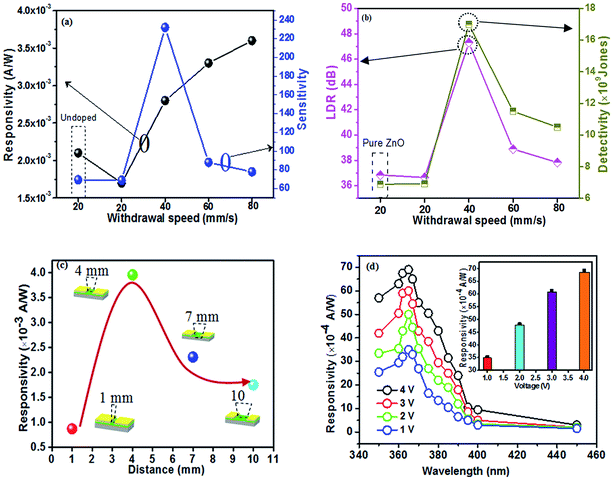 |
| | Fig. 7 Photoresponse properties of pure and Mn-doped ZnO films. (a) Responsivity and sensitivity, (b) linear dynamic range (LDR) and detectivity, (c) responsivity as a function of distance between Au electrodes for MZO films at 40 mm s−1, (d) responsivity as a function of voltage. | |
Table 1 Comparison of the rise and fall time of ZnO films based on UV photodetectors
| Materials |
Bias (V) |
λ (nm) |
R (×10−3 A W−1) |
τr (s) |
τf (s) |
Ref. |
| Mn-doped ZnO films at 40 mm s−1 |
3 |
365 |
2.75 |
1.871 |
3.309 |
This work |
| Sb-doped ZnO films |
5 |
365 |
1000 |
11.35 |
17.9 |
48 |
| ZnO films |
10 |
365 |
1500 |
29 |
29 |
49 |
| ZnO NRs |
5 |
365 |
65 |
7 |
29 |
50 |
| Mn-doped ZnO NRs |
5 |
365 |
30 |
2.75 |
16.8 |
50 |
| ZnO NWs |
1 |
365 |
— |
150 |
800 |
11 |
| Ga-doped ZnO NSs |
1 |
370 |
0.0723 |
2.45 |
4 |
51 |
4. Conclusions
In summary, metal–semiconductor–metal (MSM) Ultraviolet (UV) photodetectors (PDs) based on Mn-doped ZnO (MZO) films have been fabricated using sol–gel dip coating method and the effect of withdrawal speeds (WS: 20, 40, 60 and 80 mm s−1) on the properties of MZO films were discussed by various technologies. The results indicated that crystallinity of films is affected by the withdrawal speed and MZO films deposited at 40 mm s−1 show the best crystallinity and largest crystallite size, due to the appropriate film thickness. The formed Au/MZO/Au PDs suggest that films prepared at 80 mm s−1 show the highest photocurrent and dark current, corresponding to 2.9 × 10⁻⁵ and 3.7 × 10⁻⁷ A, respectively. PDs based on MZO films deposited at 40 mm s−1 show superior properties in response time and recovery time, and response time is 1.871 s and recovery time is 3.309 s at 365 nm for 3 V bias, which is suitable for practical applications.
Conflicts of interest
There are no conflicts to declare.
Acknowledgements
This work was supported by Natural Science Foundation of China (NSFC) No. 11675029 and Program of Science and Technology Department of Sichuan Province No. 2018JY0453, and Project of Sichuan Provincial Department of Education No. 2018Z073.
References
- A. G. Ardakani, M. Pazoki and S. M. Mahdavi, Appl. Surf. Sci., 2012, 258, 5405–5411 CrossRef.
- M. Razeghi and A. Rogalski, J. Appl. Phys., 1996, 79, 7433–7473 CrossRef CAS.
- Y. Liu and C. R. Gorla, J. Electron. Mater., 2000, 29, 69–74 CrossRef CAS.
- E. Monroy, J. A. Garrido and I. Izpura, Appl. Phys. Lett., 1997, 71, 870–872 CrossRef.
- T. N. Oder, J. Li and J. Y. Lin, Appl. Phys. Lett., 2000, 77, 791–793 CrossRef CAS.
- O. Katz, V. Garber and B. Meyler, Appl. Phys. Lett., 2001, 79, 1417–1419 CrossRef CAS.
- B. Sun, Y. Sun and C. Wang, Small, 2018, 14, 1703391 CrossRef PubMed.
- M. Badila, G. Brezeanu and J. Millan, Diamond Relat. Mater., 2000, 9, 994–997 CrossRef CAS.
- T. H. Eom and J. I. Han, Appl. Surf. Sci., 2018, 428, 233–241 CrossRef CAS.
- S. Huang, N. Yu and T. Wang, Funct. Mater. Lett., 2018, 11, 1850045 CrossRef CAS.
- W. H. Chen, C. C. Su and H. H. Hsieh, RSC Adv., 2016, 6, 91216–91224 RSC.
- S. Yu, L. Ding, H. Zheng and C. Xue, Thin Solid Films, 2013, 540, 146–149 CrossRef CAS.
- P. S. Shewale and Y. S. Yu, Ceram. Int., 2017, 43, 4175–4182 CrossRef CAS.
- M. Kumar, V. Bhatt, A. C. Abhyankar and J. Kim, Sens. Actuators, A, 2018, 270, 118–126 CrossRef.
- S. Safa, S. Mokhtari and A. Khayatian, Opt. Commun., 2018, 413, 131–135 CrossRef CAS.
- S. Husain, L. A. Alkhtaby, E. Giorgetti and A. Zoppi, J. Lumin., 2014, 145, 132–137 CrossRef CAS.
- H. B. Ruan, L. Fang, D. C. Li and M. Saleem, Thin Solid Films, 2011, 519, 5078–5081 CrossRef CAS.
- L. Fanni, B. A. Aebersold and D. T. L. Alexander, Thin Solid Films, 2014, 565, 1–6 CrossRef CAS.
- Y. C. Kong, D. P. Yu, B. Zhang and W. Fang, Appl. Phys. Lett., 2001, 78, 407–409 CrossRef CAS.
- Q. B. Ma, Z. Z. Ye and H. P. He, J. Cryst. Growth, 2007, 304, 64–68 CrossRef CAS.
- K. H. Tam, C. K. Cheung and Y. H. Leung, J. Phys. Chem. B, 2006, 110, 20865–20871 CrossRef CAS PubMed.
- T. V. Torchynska and G. Polupan, J. Mater. Sci.: Mater. Electron., 2018, 29, 15458–15463 CrossRef CAS.
- P. Jongnavakit, P. Amornpitoksuk and S. Suwanboon, Thin Solid Films, 2012, 520, 5561–5567 CrossRef CAS.
- S. Aydemir, Vacuum, 2015, 120, 51–58 CrossRef CAS.
- S. Aydemir and S. Karakaya, J. Magn. Magn. Mater., 2015, 373, 33–39 CrossRef CAS.
- S. Alavi, H. Bazrafshan and M. Nikazar, J. Sol-Gel Sci. Technol., 2016, 81, 652–661 CrossRef.
- M. Guglielmi, P. Colombo and F. Peron, J. Mater. Sci., 1992, 27, 5052–5056 CrossRef CAS.
- P. Yimsiri and M. R. Mackley, Chem. Eng. Sci., 2006, 61, 3496–3505 CrossRef CAS.
- N. Barati, M. A. F. Sani and H. Ghasemi, Appl. Surf. Sci., 2009, 255, 8328–8333 CrossRef CAS.
- H. Y. Xu, Y. C. Liu and C. S. Xu, J. Chem. Phys., 2006, 124, 074707 CrossRef CAS PubMed.
- M. Ohyama and H. Kozuka, Thin Solid Films, 1997, 306, 78–85 CrossRef CAS.
- L. H. Xu and X. Y. Li, Appl. Surf. Sci., 2011, 257, 4031–4037 CrossRef CAS.
- F. Wang, M. Z. Wu and Y. Y. Wang, Vacuum, 2013, 89, 127–131 CrossRef CAS.
- G. Srinivasan and J. Kumar, J. Cryst. Growth, 2008, 310, 1841–1846 CrossRef CAS.
- R. Rajalakshmi and S. Angappane, J. Alloys Compd., 2014, 615, 355–362 CrossRef CAS.
- Z. N. Kayani, T. Afzal and S. Riaz, J. Alloys Compd., 2014, 606, 177–181 CrossRef CAS.
- R. Rajalakshmi and S. Angappane, Mater. Sci. Eng., B, 2013, 178, 1068–1075 CrossRef CAS.
- G. Xiong, U. Pal and J. G. Serrano, Phys. Status Solidi C, 2006, 3, 3577–3581 CrossRef CAS.
- Y. Guo, X. Cao, X. Lan, C. Zhao, X. Xue and Y. Song, J. Phys. Chem. C, 2008, 112, 8832–8838 CrossRef CAS.
- P. Kumar and B. K. Singh, Appl. Phys. A: Mater. Sci. Process., 2016, 122, 740–751 CrossRef.
- W. M. Hlaing Oo and L. V. Saraf, J. Appl. Phys., 2009, 105, 013715 CrossRef.
- H. S. Kim, M. Patel, H. H. Park and A. Ray, ACS Appl. Mater. Interfaces, 2016, 8, 8662–8669 CrossRef CAS PubMed.
- Y. Wu and K. V. Rao, IEEE Trans. Magn., 2010, 46, 2152–2155 CAS.
- P. Gu, X. H. Zhu and D. Y. Yang, Appl. Phys. A: Mater. Sci. Process., 2019, 125, 50–57 CrossRef.
- P. Kumar and R. Singh, J. Appl. Phys., 2018, 123, 054502 CrossRef.
- Z. Yang and M. Q. Wang, J. Mater. Chem. C, 2014, 2, 4312–4319 RSC.
- W. T. Cheng and L. B. Tang, RSC Adv., 2016, 6, 12076–12080 RSC.
- S. V. Mohite and K. Y. Rajpure, Opt. Mater., 2014, 36, 833–838 CrossRef CAS.
- C. Portesi and L. Lolli, Eur. Phys. J. Plus, 2015, 130, 45–52 CrossRef.
- C. O. Chey, X. Liu and H. Alnoor, Phys. Status Solidi RRL, 2014, 9, 87–91 CrossRef.
- S. J. Young and Y. H. Liu, Microelectron. Eng., 2015, 148, 14–16 CrossRef CAS.
|
| This journal is © The Royal Society of Chemistry 2019 |
Click here to see how this site uses Cookies. View our privacy policy here. 
 Open Access Article
 This Open Access Article is licensed under a Creative Commons Attribution-Non Commercial 3.0 Unported Licence
 *a
*a