
 Open Access Article
 This Open Access Article is licensed under a Creative Commons Attribution-Non Commercial 3.0 Unported Licence
First-principles study of Ni adatom migration on graphene with vacancies
E. E. Hernández-Vázquez a,
F. Munozbc,
S. López-Moreno*d and
J. L. Morán-Lópeza
a,
F. Munozbc,
S. López-Moreno*d and
J. L. Morán-Lópeza
aDivisión de Materiales Avanzados, IPICYT, Camino a la Presa San José 2055, San Luis Potosí, S.L.P. 78216, Mexico
bDepartamento de Física, Facultad de Ciencias, Universidad de Chile, Santiago, Chile
cCentro para el Desarrollo de la Nanociencia y la Nanotecnología (CEDENNA), Santiago, Chile
dCONACYT – División de Materiales Avanzados, IPICYT, Camino a la Presa San José 2055, San Luis Potosí, S.L.P. 78216, Mexico. E-mail: sinhue.lopez@ipicyt.edu.mx
First published on 14th June 2019
Abstract
A theoretical study based on first-principles calculations about the interaction and diffusion of Ni atoms on pristine graphene and graphene with a single vacancy is presented. In the first case, we explored the structural changes due to the adsorption of Ni on graphene and the effects on the electronic structure. In the case of graphene with a vacancy, we analyzed the impact of the adsorbed Ni atom on the distortion of the graphene structure and how it depends on the distance from the graphene defect. In the analysis, we observed the changes in the electron localization function and the charge density. By knowing the interaction map of Ni with graphene, and the structural changes of the network, we performed energy barrier calculations within the climbing image nudged elastic band methodology to study the nickel diffusion. Finally, we explored how the vacancy and structural distortions affect the minimum energy paths and the saddle points for nickel moving away, around, and towards the vacancy.
1 Introduction
Graphene has attracted great attention from both experimentalists and theoreticians since its experimental synthesis in 2004.1–3 This material shows a unique sub-lattice symmetry and is a zero-gap semiconductor with high electron mobility, reaching 1 to 5 × 104 cm2 V−1 s−1 at room temperature with an intrinsic mobility limit of 2 × 105 cm2 V−1 s−1.4 Graphene also shows interesting physical phenomena such as the anomalous quantum Hall effect and the presence of massless Dirac fermions.5The understanding of the role of defects in the properties of graphene and carbon-based nanostructures has become essential for the development of several applications and devices based on carbon, such as lithium storage in nanotube-based batteries, environmental applications, and catalytic growth, to name a few.6–9 In this sense, it is well known that pristine graphene does not present magnetic properties, but the introduction of defects can be a method to induce that behavior.10 Some theoretical studies have been devoted to the study of this phenomenon.11–13 Graphene magnetism can be achieved with single or double vacancies and Stone–Wales defects; being the most common and stable the single vacancy.14 These vacancies can promote π long-range order magnetism; ferromagnetic or antiferromagnetic, depending on the defect sublattice. Even non-magnetic defects have been predicted to display a short-range magnetic order, although measurements of magnetic states have produced contradictory results in graphene oxides.15,16 Substitutional atoms in graphene by transition metals (TM), from the 4d and 5d rows, behave similarly regarding their geometrical and magnetic properties. In the case of 3d TM impurities, a larger magnetic moment at the adatom was found for Cr and Mn, which couple antiferromagnetically to the neighbor C atoms.17 In this sense, there is a great interest in understanding the characteristics that govern the interaction between transition metals and graphene.18–21 In another way, besides the interaction of graphene with TM, very recently it was reported the interplay of transition metals with other 2D materials such as C3N, germanene, phosphorene, stanene, and tin sulfide, to name a few.22,23
A widely studied phenomenon in which the scattering of conduction electrons by magnetic impurities increases as the temperature is lowered, depends strongly on the density of states at the Fermi energy. First-principle calculations have predicted that magnetic impurities on the free-standing graphene exhibit the Kondo effect and that their presence control the density of electronic states at the Fermi level.24
According to experimental reports, intrinsic defects in crystals are not always stationary, and their migration can have a significant influence on the properties of a defective crystal. In graphene, vacancies or Stone–Wales defects, can change not only the properties of graphene itself but the mobility of adsorbed atoms, which could diffuse parallel to the graphene plane. The diffusion of adatoms on pristine graphene require less energy than in graphene with a vacancy due to the strong covalent bonds between the adatoms and the C atoms from the vacancy.25 That motion is generally governed by an activation barrier that depends on the type of defect and exponentially increases with temperature.16
The migration of some adatoms such as Au and Pt over graphene was followed by means of high-resolution transmission electron microscopy (TEM).26 In those cases, in which TM metals atoms are adsorbed on a vacancy, the activation energy for the in-plane migration of both species on defective graphene was 2.5 eV (at 600 °C), which indicates covalent bonding between metal and carbon atoms from the vacancy. Furthermore, the linear diffusion of these atoms along the open edge of a graphene layer occurs at slightly lower activation energy.26 On the other hand, it was found that diffusion of metal atoms in curved layers of carbon nanotubes is somewhat faster than in planar graphene. This topic gave rise to the development of theoretical works within the density functional theory (DFT) in which the formation of small gold clusters and their diffusion in graphene were studied, both parallel to the graphene plane and on the edges of graphene.27,28
On the other hand, adsorption and migration energies for 3d transition metal atoms on graphene have been reported using DFT.17,25,29–37 It was found that most of the transition metals studied have the highest adsorption energy in a hole site (H) in the graphene network [see Fig. 1(a)], except Cr. It was reported that the migration energy barrier for TM adatoms on graphene is in the range between 0.2 to 0.8 eV, which indicate that the adatoms can move over graphene at room temperature.25 On the other hand, Ni-based clusters are promising catalysts in terms of cost and outstanding activity compared with noble-metals.38 Furthermore, very recently a study of the interaction of Ni clusters in graphene with vacancies was reported, where the diffusion of Ni nanoclusters on graphene with random vacancies at high temperatures was reported.39
 | ||
| Fig. 1 (a) Three possible sites where a Ni atom can be adsorbed on a hexagon of the pristine graphene layer: top (T), bridge (B), and hollow (H). (b) Graphene 8 × 8 supercell with a vacancy, the letters from a to o show the possible non-equivalent sites where Ni can be adsorbed. Numbers 1 to 3 stand for the C atoms around the vacancy. | ||
In this work, we present a first-principles study of the structural and electronic changes that occur when Ni is adsorbed on graphene and graphene with a single vacancy. We analyzed the structural effects such as the deformation of the system in the presence of extrinsic defects and their effect on the electronic structure. In particular we analyzed how the Jahn–Teller distortion, present in the single vacancies in graphane, change in the presence of chemisorbed Ni. We also calculated how the adsorption energies depend on the distance between the adsorbed atom and the vacancy, and the energies required for the diffusion of Ni over pristine graphene and graphene with a single vacancy. We explored several paths over the surface to identify the influence of the topography and the deformation of the graphene layer on the energy barriers.
The present work is organized as follows. In Section 2 we give a detailed description of the computational methods used in this report. A brief description of graphene and graphene with a vacancy is given in Section 3.1 in order to substantiate our work and be able to compare our results with those of the literature. The results and discussion of the Ni atoms adsorbed on graphene and graphene with a vacancy are described in Section 3.2. Calculations of the energy barriers of Ni on graphene are presented in Section 3.3. Finally, we discuss and summarize the primary results of this work in Section 4.
2 Computational details
Calculations of the total energy were performed within the framework of the spin-polarized density functional theory (DFT)40 and the projector-augmented wave (PAW)41,42 method as implemented in the Vienna Ab initio Simulation Package (VASP).43–46 A plane-wave energy cutoff of 500 eV was used to ensure high precision in our calculations. The exchange–correlation energy was described within the generalized gradient approximation (GGA) in the Perdew–Burke–Ernzerhof prescription.47Monkhorst–Pack scheme was employed to discretize the Brillouin-zone (BZ) integrations48 with a mesh of 11 × 11 × 1 for the primitive unit cell (2 atoms) of graphene; this ensures precision of the energy to less than 1 meV per atom. For the simulation of graphene with a vacancy and the adsorption of a Ni atom on graphene, an 8 × 8 × 1 (128 C atoms) supercell was used. For this large supercell of graphene, the distance between the vacancy and its image due to the periodic conditions is ≈20 Å and represents a concentration of vacancies or adatoms of 1/128. For this large supercell, the calculations were performed with just one k-point. It is worth mentioning that the calculations were made by fixing the graphene cell vectors while allowing the carbon and nickel atoms to relax. The calculations of Ni adsorbed on graphene and graphene with a vacancy were performed without fixing the magnetic moment. In particular we find that the magnetic moment of Ni is zero in the lowest state energy, as reported in the literature.33 Likewise, we find that there is no magnetization in the Ni/graphene system for Ni adsorbed on the vacancy, but there is a small magnetic moment in some cases when the Ni atom is adsorbed outside the vacancy. This point will be discussed in the next section. Methfessel–Paxton smearing49 was used with an n value of 2. A value of 0.02 eV was chosen for the width of the smearing.
The adsorption energy, Ead, for Ni atom on graphene with and without a vacancy is calculated as follows
| Ead = EC/Ni − EC − ENi, | (1) |
We define the vacancy deformation, Δi (%), due to the adsorption of the Ni atom at the i site on graphene with a vacancy [see Fig. 1(b)] by
 | (2) |
The charge redistribution due to the adsorption process of Ni on graphene is used to analyze the nature of electron transfer. The charge density difference is calculated as follows
| Δρ(r) = ρC/Ni(r) − ρC(r) − ρNi(r), | (3) |
The dissociation paths and diffusion barriers are determined by using the nudged elastic band (NEB) method.50,51 The NEB is a method used to find saddle points and minimum energy paths between known reactants and products. The method works by optimizing a number of intermediate images along a reaction path. Each image finds the configuration with the lowest energy while maintaining equal spacing to neighboring images. The search of the saddle point has been refined by using the climbing image NEB method.52,53 The number of images used in the calculation was chosen according to the complexity of the geometry of the system.
3 Results and discussion
3.1 Graphene with and without a vacancy
As a first step and in order to test the accuracy of our method, we calculated first the properties of graphane without and with a vacancy, and compare our results with those published with similar theories.3,33 Graphene has a hybridized sp2 bonding. It shows three in-plane σ bonding orbitals and a π orbital perpendicular to the plane. While the strong σ bonds work as the rigid backbone of the hexagonal structure, the out-of-plane π bonds control the interaction between different layers in graphite,3 and the interaction with adsorbed atoms. We have used electron localized function (ELF) maps to observe the bonding patterns within the graphene network. As shown in the right panel of Fig. 2, the areas with blue tonality represent high density (bonding), and red zones denote an electronic charge density deficiency. On Fig. 2(c), we show the case of pristine graphene with covalent C–C bonds with perfectly marked electron states. In our calculations, we obtain a graphene C–C interatomic distance of 1.425 Å, in good agreement with the value of 1.43 Å from ref. 33. | ||
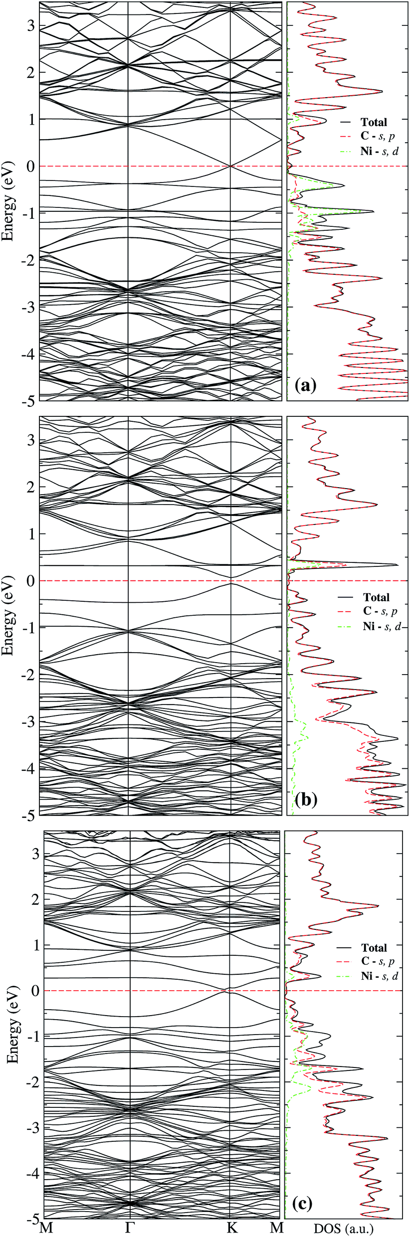
| Fig. 2 Band structure and density of states for (a) pristine graphene and (b) graphene with a vacancy. The dashed line at 0 eV marks the Fermi level. In the right panel, we present the results of the electron localization function (ELF) contour plots for (c) pristine graphene and (d) graphene with a vacancy. In the color bar 0 (1) means the absence (presence) of electronic charge. | ||
The simplest defect in any material is the absence of an atom in the perfect lattice. Single vacancy (SV) in graphene has been observed experimentally by Transmission Electron Microscopy (TEM) and Scanning Tunneling Microscopy (STM).16,54 As it is shown on Fig. 2(d), C atoms around the SV undergoes a Jahn–Teller distortion which leads to the formation of a weak σ bond between C atoms 1 and 3 (see Fig. 1) while atom 2 remains with a dangling bond. This vacancy with 5–9 ring structure is called a V1(5–9) defect.16 Graphene with the vacancy V1(5–9) is 332 meV more stable than graphene with a vacancy with C3V symmetry. In our results, the distance among C atoms 1 and 3 is d1–3 = 2.055 Å, while the distance d1–2 = d2–3 = 2.588 Å, in good agreement with respective values (1.97 and 2.58 Å) published recently in ref. 12. This distortion produces changes in the interatomic distances around the V1(5–9) defect from 1.393 to 1.4767 Å to first neighbors, and from 1.4123 to 1.4534 Å to second neighbors. Fig. 2(a) and (b) presents the band structure and total density of electronic states (DOS) of pristine graphene and with a single vacancy. One observes that the zero energy gap at the Fermi energy, characteristic of graphene, gets populated by the presence of vacancies, even at such a low concentration of 0.008 (1/128). As can be seen in the electronic structure of Fig. 2(b), there is a significant difference in the up and down states, mainly around the Fermi level and at 2 eV. This indicates that there is a magnetization, which is distributed mostly in the C atom with the dangling bond and less in C atoms with the weak σ bond of the vacancy. In our case, we find a total magnetic moment of 1.16 μB, in fair agreement with magnetic moment (1.45–1.53 μB) from ref. 10.
3.2 Ni adsorption on graphene
Recently, it has been reported that transition metal (TM) atoms can be adsorbed in three different sites on graphene.25,30,31,33,55,56 The possible adsorption sites have been labeled as H, T, and B, which correspond to the Ni atom adsorbed on a carbon hexagon, on top of a C atom, and in a bridge between two C atoms, respectively, see Fig. 1(a). First, we performed the calculations of the adsorption of Ni atom on pristine graphene in order to understand the effects of the Ni adsorbed on graphene with a vacancy. The adsorption energy, Ead, the distance between Ni atom and the nearest graphane C atoms, dNi–C, and the height measured from the clean graphene plane to the Ni atom, z, are listed on Table 1. As expected, the strongest adsorption energy corresponds to Ni adsorbed on an H site, with a difference of 236 meV with respect to the B site and 313 meV to the T site. These results are in agreement with those reported in the literature.25,33,55 Note that Ni is coordinated with six, two, and one carbon atoms in H, B, and T site, respectively.| Site | Ead (eV) | dNi–C (Å) | z (Å) |
|---|---|---|---|
| T | −1.180 | 1.853 | 1.853 |
| B | −1.257 | 1.937 | 1.912 |
| H | −1.493 | 2.113 | 1.571 |
The adsorption of Ni on pristine graphene induces local deformations on the C-network, mainly in the carbon bonds formed by the atoms linked to Ni and the bonds between second C neighbors. In the case of the adsorption of Ni on T site the C–C interatomic bond distance between the atom below and its neighbors increase from 1.425 to 1.441 Å. For adsorption on a B site, the bridge that is formed by the two carbon atoms is deformed to 1.440 Å and a C–C distance of 1.439 Å between the bridge atoms and its other two neighbors. Whereas in the H site the distance between the hexagon atoms is 1.441 Å and the distance between these atoms and the other two neighbors have a C–C distance of 1.428 Å. Thus, in the last case, the Ni adsorption produces the less lattice deformation. This is directly related with the smallest z and largest dNi–C values, (see Table 1). Since H is the most relevant adsorption site, from now on, the only adsorption on this kind of sites will be discussed.
The structural changes in graphene due to the Ni adsorption have a direct effect on the electronic structure. This is illustrated in Fig. 3. The first column corresponds to the absorption of Ni on a perfect C-lattice. The columns (b) to (d) contain the information for the cases where the Ni atom is adsorbed on sites a, b, and c of a defected lattice [see Fig. 1(b)], which will be discussed later. In the top figures, we display the contour plots of the ELF corresponding to the different cases. Here, we see that in site H, the charge distribution is modified mainly around the six C nearest neighbors and only subtle changes are noticed in the second neighbors.
 | ||
| Fig. 3 The first row shows a contour plot of the Electron Localization Function, ELF. The colors used for ELF are the same as in Fig. 2. The second row shows the charge density difference, Δρ(r), among the charge density of the graphene/Ni system and the individuals charge densities of graphene and Ni. Cyan and purple colors correspond to positive and negative values. The charge density differences were computed at 0.01 eV Å−3. The first column corresponds to site H of pristine graphene, and columns 2–4 to sites a, b, and c from graphene with a vacancy, see Fig. 1(b). | ||
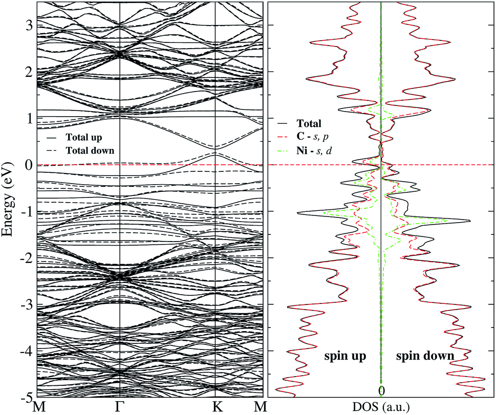
The lower row of Fig. 3 corresponds to the iso-surfaces of the charge density differences, Δρ(r) (see Section 2). According to this figure, there is a small change in the charge density up to the second neighbors for an iso-surface level of 0.01 eV Å−3. Furthermore, the band structure presented in Fig. 4(a) shows that Ni changes the electronic structure of graphene, mainly in the range from −2 eV up to the Fermi level, where there is a hybridization of states from both species that give rise to the formation of the bonds between Ni and carbon atoms. New bands appear in that range of energy, a fact that is reflected in the DOS, mainly from −2 eV to the Fermi level, and at 1 eV. As we can see from the DOS, these occupations belong to the s and d states from Ni. Similar results were reported in the literature.33,36 It was not observed a difference in the up and down channels in the electronic structure.
 | ||
| Fig. 4 Band structure, right-hand side, and electronic density of states, left-hand side, of Ni adsorbed on an H site of pristine graphene (a). Insets (b) and (c) correspond to Ni adsorbed on sites a and b of graphene with a single vacancy. The dashed line at 0 eV marks the Fermi level. | ||
In the case of graphene with a vacancy, Fig. 1(b) shows with letters from a to o the inequivalent sites of the graphene supercell where the Ni atom can be adsorbed. In that figure, sites c′ and f′ are equivalent with sites c and f, respectively. Furthermore, the numbers 1 to 3 are used to indicate which atoms around the vacancy move away from the graphene layer due to the adsorption or diffusion of Ni over graphene. Also, we use numbers 1 to 3 to identify the atoms in the Jahn–Teller distortion. Table 2 lists the main results for the adsorption of Ni on graphene with a vacancy, similarly to the results of Table 1 with a few differences. Here dV indicates the distance from Ni adsorbed on a graphene hexagon to the position of Ni when is adsorbed on the vacancy. This is a measure of the influence of the vacancy in the adsorption energy on a hexagonal site away from the vacancy. Δi indicates the perimetrical deformation around the vacancy due to the Ni adsorption in comparison to the clean graphene with a vacancy. Also is listed the magnetic moment of the respective carbon atom with the dangling bond of the vacancy, which is the carbon atom with the largest magnetic moment among the other C atoms, and the magnetic moment of Ni atom.
| Site | dV (Å) | Ead (eV) | 〈dNi–C〉 (Å) | z (Å) | Δi (%) | mC (μB) | mNi (μB) |
|---|---|---|---|---|---|---|---|
| a | 0 | −6.713 | 1.796 | 1.363 | 0.088 | 0 | 0 |
| b | 3.001 | −2.304 | 2.110 | 1.895 | 0.469 | 0 | 0 |
| c | 3.688 | −1.778 | 2.121 | 1.557 | 0.399 | −0.409 | 0.323 |
| d | 5.112 | −1.604 | 2.122 | 1.571 | 0.229 | −0.414 | 0.217 |
| e | 5.620 | −1.599 | 2.127 | 1.523 | 0.106 | 0.423 | −0.256 |
| f | 6.216 | −1.565 | 2.118 | 1.557 | 0.029 | 0.397 | −0.184 |
| g | 7.163 | −1.430 | 2.113 | 1.580 | 0.047 | 0 | 0 |
| h | 7.491 | −1.727 | 2.119 | 1.514 | 0.141 | 0.380 | −0.010 |
| i | 7.918 | −1.536 | 2.122 | 1.537 | 0.076 | 0.403 | −0.195 |
| j | 8.670 | −1.501 | 2.120 | 1.544 | 0.053 | 0.394 | −0.149 |
| k | 9.331 | −1.498 | 2.117 | 1.583 | 0.094 | −0.376 | 0.092 |
| l | 9.964 | −1.450 | 2.116 | 1.547 | 0.070 | 0 | 0 |
| m | 9.970 | −1.518 | 2.116 | 1.571 | 0.088 | 0.385 | −0.100 |
| n | 10.277 | −1.519 | 2.121 | 1.549 | 0.076 | 0.394 | −0.183 |
| o | 11.400 | −1.466 | 2.114 | 1.567 | 0.029 | 0.348 | 0.002 |
According to Table 2 the lowest adsorption energy belongs to nickel adsorbed on the vacancy (site a), with a value of −6.713 eV. This indicates that once a Ni atom is adsorbed on the vacancy, a very high temperature would be required to break the Ni–C bonds. A value of ≈7 eV was reported in ref. 25 using a 7 × 7 × 1 cell, where a series of TM atoms were adsorbed on single and double vacancies of graphene. In this configuration, Ni is strongly bonded to three carbon atoms with an interatomic Ni–C distance of 1.796 Å, which is much smaller than the distances listed on Table 1. Also, we find that in this site carbon atoms 1–3 are pulled 0.431 Å outward of the layer, by the Ni atom.
When Ni is adsorbed over a hexagon, away from the vacancy, there are significative differences on the adsorption energy, and in the deformation of the structure, depending on the location of the Ni atom with respect to the vacancy. In general, when Ni is adsorbed on a C hexagon, the graphene layer undergoes a deformation, mostly in the bond distances around the vacancy. In almost all cases, the C atom with the dangling bond is displaced away from the graphene plane. Besides, depending on the position of the Ni atom, the Jahn–Teller distortion of the vacancy can change from the initial configuration to minimize the energy of the system. That is, in some cases the minimum energy state of the Ni/graphene system will be given when atoms 1 and 3 of the vacancy form the weak σ bond, while in other cases the same bond will be formed with atoms 2 and 3, as seen in Fig. 5.
 | ||
| Fig. 5 Magnetization charge density of pristine graphene with the vacancy (a), and Ni adsorbed on graphene with a vacancy on sites (b) c, (c) d, (d) e, (e) f, and (f) i. The isosurface value used was 0.013 e Å−3. Cyan and purple colors correspond to positive and negative values. | ||
To have a general picture, Fig. 6 shows the variation of the (a) adsorption energy, (b) the average of the Ni–C distance, (c) the distance from Ni to the clean graphene plane, and (d) the perimetrical deformation around the vacancy, as a function of the distance between the Ni atom adsorbed on a hexagon, and the position where a Ni atom is adsorbed on the vacancy, dV. As can be observed in Fig. 6(a), the Ni atom bonds weaker as the Ni atom is adsorbed further away from the vacancy. In the case of 〈dNi–C〉, when Ni is on any C hexagon, the values are around 2.119 Å, as compared to 1.796 Å that corresponds to the case when Ni is adsorbed at the vacancy. These two curves show that, for Ead and 〈dNi–C〉, there is a significant difference only when the Ni atom is in the vacancy or adsorbed in any other hexagon, regardless of the distance of the Ni atom to the vacancy. The variation of z with dV is very similar to the trend in Fig. 6(a) and (b). However, in this case there is a marked difference when the Ni atom is adsorbed in site b (dV = 3.001 Å), because the C atom 2, which has a dangling bond, moves out of the graphene plane. This effect is produced by the fact that this atom is only bonded with other two C atoms. This deformation was also observed when Ni is adsorbed on bilayer graphene with a single vacancy.33
 | ||
| Fig. 6 (a) Variation of the adsorption energy (Ead), (b) average C–Ni distance (〈dNi–C〉), (c) distance from Ni to the clean graphene layer (z), and (d) deformation area (Δi), with respect to the distance from the Ni atom adsorbed on site a and Ni adsorbed at any of the other different sites (dV) from Fig. 1(b). | ||
According to Fig. 6(d) Δi reaches its maximum when the Ni is in site b, for the reason mentioned above. As the distance dV increases this deformation decreases to 0.029, point in which the Ni atom is at the site f. From this point on, it reaches an average value of 0.0703%.
From Fig. 3(b), one observes that the ELF contour plot shows a symmetrical redistribution of the electronic density around the vacancy due to the adsorption of Ni on site a. Whereas, the Δρ(r) shows that, in general, this electronic redistribution affects up to second neighbors, as shown in the second row of Fig. 3(b). On the other hand, the band structure and the DOS from Fig. 4(b) show the splitting of the bands in the deeper states. More importantly, is the energy shift in the bands around the Fermi level due to the Ni adsorption on the vacancy. This shift in the bands can be seen by comparing the band structure of clean graphene with a vacancy [see Fig. 2(b)] and with Ni adsorbed on the vacancy [Fig. 4(b)]. It is noteworthy that at 0.34 eV a new band appears corresponding to the d states of the Ni. At this same energy, a large peak appears in the DOS due to the coupling of the Ni and C states.
When Ni is adsorbed outside the vacancy in positions b to o the picture is quite different. According to the ELF contour plots of the first row of Fig. 3(c) and (d), the charge deficiency space take a similar shape to the pure graphene with the vacancy of Fig. 2(d). The redistribution of the charge has a reflection symmetry when the adsorption takes place in the b site, while the other ones do not present a particular symmetry. Thus, the structural deformation observed in Fig. 6(d) for Ni adsorbed on sites b, and c, is completely due to the fact that the adsorption of Ni deforms the structure of the vacancy. On the other hand, as seen in Fig. 3(c) and (d), from the second row, the redistribution of the charge density difference spreads to a longer distance when Ni is adsorbed at site c than in b.
Regarding the magnetic moment listed in Table 2 for Ni adsorbed in some sites out of the vacancy, it is observed that the carbon atom with the dangling bond has a value that is around 0.4 μB. Close to the value of the same atom in the graphene with a vacancy (0.54 μB). Other carbon atoms present a magnetic moment but are quite small. On the other hand, the magnetic moment of Ni strongly depends on its position with respect to the vacancy. To make it clearer, Fig. 5 shows the magnetization of the charge density for the Ni atom adsorbed at several sites out of the vacancy. The greater contribution comes from the C atom with the dangling bond. One can observe this information in the band structure and DOS of Fig. 7 for Ni adsorbed on site c. In this case, there is a separation in the up and down states similar to that observed in graphene with the vacancy in Fig. 2(b). However, this splitting is more marked from −2 to 1 eV, corresponding to the s and d states of Ni. We can also see that in this energy range there are now new bands belonging to the Ni atom, which make a greater difference in the up and down states. Thus, we can see that the Ni adsorption favors graphene magnetization with the vacancy by increasing the population of states around the Fermi level. We observe a similar behavior for Ni adsorbed on other sites away from the vacancy. Thus, the reactivity of the Ni/graphene system will change depending on the position of the Ni with respect to the vacancy. Which can have a major impact on catalysis and electronics.
 | ||
| Fig. 7 Band structure and electronic density of states for Ni adsorbed on site c of graphene with a single vacancy. The dashed line at 0 eV marks the Fermi level. | ||
3.3 Ni diffusion on graphene with and without vacancies
The energy barriers that prevent the Ni atom motion over the graphene layer with and without a vacancy, were calculated for several possible initial and final states according to the Ni positions illustrated in Fig. 1(b) and the calculated adsorption energies from Tables 1 and 2 The results obtained using the climbing image nudged elastic band (cNEB) method are listed in Table 3. In the absence of experimental evidence, we compare our results to other theoretical reports.| IS | FS | zTS (Å) | dTS (Å) | Ebarr (meV) | |
|---|---|---|---|---|---|
| Graphene | H | H | 1.950 | 1.934 | 224 |
| Graphene wV | b | a | 2.176 | 1.823 | 30 |
| c | a | 1.833 | 1.862 | 103 | |
| c | c′ | 1.943 | 1.918 | 287 | |
| c′ | b | 1.751 | 1.939 | 260 | |
| d | b | 1.980 | 1.924 | 244 | |
| d | c′ | 1.835 | 1.936 | 340 | |
| f | c | 1.930 | 1.934 | 212 | |
| f′ | e | 1.888 | 1.918 | 188 | |
| g | d | 2.000 | 1.926 | 215 | |
| h | f′ | 1.871 | 1.928 | 226 | |
| h | d | 1.858 | 1.943 | 240 | |
| i | j | 1.973 | 1.930 | 291 | |
| j | f′ | 1.926 | 1.936 | 229 | |
| k | g | 1.861 | 1.923 | 248 | |
| k | h | 1.831 | 1.944 | 298 | |
| m | h | 1.846 | 1.932 | 268 | |
| m | j | 1.907 | 1.930 | 213 | |
| n | l | 1.793 | 1.948 | 148 | |
| o | k | 1.872 | 1.933 | 294 |
First, we calculated the energy barrier that the Ni atom encounters when moving over perfect graphene from one hexagon to another, passing over two carbon atoms [Fig. 1(a)]. To perform this movement, the energy barrier obtained in our calculations was 244 meV. This is in agreement with previous calculations,25 where the energy barrier for transition metal atoms (Sc–Zn, Pt, Au) that move from an H site to another, are in the range of 0.2–0.8 eV. In all the states for that path, the Ni magnetic moment is zero, and the adsorption of Ni produces a small distortion of the structure along the H–H path. The larger distortion is produced when Ni is in the B site, that corresponds to the saddle point. Here, the C atoms linked to Ni move 0.161 Å above the graphene plane. Thus, the path followed by Ni in its motion on graphene is from one H site to another along the bridge sites.
The situation is quite different when Ni is adsorbed on graphene with a vacancy. As we saw in the previous section, when the Ni atom is adsorbed on defected graphene, the carbon atoms around the vacancy relax upward or downward the plane, depending on the particular absorption site. Furthermore, it was observed that when a nickel atom moves from an H site to another one, the energy barrier is a sum of the energy due to the Ni atom passing over two carbon atoms (B site) and the energy due to the movement of carbon atoms around the vacancy [atoms 1 to 3 from Fig. 1(b)].
When the Ni atom is adsorbed in a H site at a distance larger than 3.7 Å, the energy required to migrate to another H place, is between 200 and 300 meV. There are three exceptions; two of them smaller, corresponding to the jumps n–l and f′–e, and one with the highest energy barrier d to c′. In the first one, the Ni atom goes from the n site, which does not induce a distortion around the vacancy according to Table 2, to the l site, where C3 [see from Fig. 1(b)] moves away from the graphene plane on the opposite side of Ni. Thus, the initial movement of the Ni atom induces a small distortion of C atoms towards the l configuration, that is the reason for the small energy barrier of 148 meV. Let us recall that C atoms 1–3 around the vacancy do not undergo a distortion when Ni is adsorbed on site n. Otherwise, when Ni moves along the path f′–e the position of the C atoms around the vacancy do not suffer remarkable changes, only C2 moves down to the opposite side of Ni. That is, only one carbon atom moves in the neighborhood of the vacancy.
The highest energy barrier corresponds to the diffusion of Ni from site d to c′. Here, the Ni atom moves from a position away from the vacancy to one of the two possible sites neighboring the vacancy. This movement changes strongly the structure of the atoms that surround the vacancy. In the initial state, site d, the carbon atom 3 is out of the plane of graphene. As the Ni atom starts the movement to site c′ this C atom moves with the other carbon atoms to reach the transition state (bridge site-type) and aligns with the other C atoms in the plane. Once Ni passes from the bridge to the site c′, the carbon atom C1 and its two neighbors move out of the plane. Hence, this high energy barrier is more related to the deformation of the graphene layer.
In Fig. 8(a) and (b), we present the energies associated to the migration of a Ni atom along two trajectories that end at the vacancy a. The line in black corresponds to the path f to a crossing the site c and then continuing to the vacancy. On the other hand, the line in red corresponds to the case in which the Ni moves from site d to a. These results show that the easiest way to reach the vacancy is through the second path. In Fig. 8(b) we show the detailed behavior around the saddle (transition) points, which are marked by triangles.
 | ||
| Fig. 8 (a) Two selected minimum energy paths for a Ni atom moving across graphene to a vacancy, f to a, and d to a. Transition state points are denoted by triangles. Inset (b) shows a magnification of the paths around the saddle points. The x-axis represents the distance between the initial and final states. Open symbols stand for our static calculations while the solid ones are for results from cNEB results. Insets (c), and (d) show the positions of the atoms at some points marked in inset (a), where, the transition state (TS) is specifically indicated. | ||
In Fig. 8(c) we show the trajectory, in real space, that follows the Ni atom when it moves from site c to the vacancy a. This trajectory shows the second lowest energy barrier value, of 103 meV, which corresponds to path 1 [see Fig. 8(a)]. Here the saddle point occurs at 3.694 Å, position at which the Ni atom is located over one C atom. At this point, the carbon atoms C1 and C3 do not move away from the graphene layer while C2 moves 0.516 Å upward. In the way to the vacancy, the Ni atom moves over the carbon atoms close to C1, as seen in Fig. 8(c).
On the other hand, as shown in Fig. 8(d), when Ni moves from site b to the vacancy a, the Ni atom reaches the saddle point at a distance of 2.608 Å with respect to the initial state at site d, see Fig. 8(a); here the energy barrier is only 30 meV. Note that the saddle point is reached even before the Ni atoms moves out of the hexagon b. This energy barrier is mainly due to the movement of Ni over graphene, not due to a distortion of atoms from the vacancy.
Finally in Fig. 9, we show the results when the Ni atoms moves around the vacancy, i.e. from site c to b along c′. As presented in Fig. 9(a), the transition from site c to c′ requires to overcome an energy barrier of 287 meV. When Ni moves further from site c′ to b, there are strong changes in the vacancy structure due to the attraction exerted by the defect on the nickel atom. Thus, we see a decrease in the energy barrier when the nickel moves from position c′ to b. In the middle and lower panels Fig. 9(b)–(d), we show the real space trajectory. Here, we also give the distances from the initial point; Fig. 9(c) and (d) correspond to the transition points.
 | ||
| Fig. 9 (a) Minimum energy path for a Ni atom moving around the vacancy, from c to b. The x-axis represents the distance between the initial and final states. Open symbols stand for our static calculations while the solid ones are for results from cNEB results. In the middle and lower panels, Insets (b) to (e) show the positions of the atoms at some points marked in inset (a), where, the transition states (TS) are clearly indicated. | ||
Summarizing, we observe that a Ni atom moves from a hexagonal site away from the vacancy overcoming energy barriers in the range of 148 to 340 meV, approaching to site b or c. Finally, to reach the vacancy, the Ni atom has to overcome an energy barrier of 30 or 103 meV from those sites, respectively.
4 Conclusions
Nickel adsorption and diffusion on pristine graphene and graphene with a vacancy was explored by using first-principles calculations and the climbing image nudged elastic band method. We calculated the electronic structure within the framework of the spin-polarized density functional theory and used an 8 × 8 × 1 supercell. The band structure and the local density of states were obtained to explore the changes in the electronic states close to the Fermi energy. The electron localization function was analyzed to see the charge redistribution produced by the adsorption of a Ni atom. For the pristine graphene, we find that the highest adsorption energy is obtained when the Ni atom is adsorbed on a H site (−1.493 eV), followed by the bridge (−1.257 eV), and top sites (−1.18 eV), i.e. the system Ni/graphene becomes more stable as the number of Ni–C bonds increases. We also characterized the different bond lengths and geometrical rearrangement of the neighbor graphene atoms.Regarding the graphene with a vacancy, due to the size of the supercell, the concentration of vacancies is 1/128 and there are 15 non-equivalent sites. For the first time, a complete study of the interaction of Ni on the 15 possible sites, on and around the lattice defect. Here, the dependence of the adsorption energy, Ni–C interatomic distance, and perimetrical deformation around the vacancy, were analyzed as a function of the position at which the Ni atom is adsorbed. We found that, in most cases, the structural deformation of graphene is accompanied by magnetization of the system similar to graphene with the vacancy. Likewise, we found that the Jahn–Teller distortion of the vacancy changed depending on the position of the Ni atom in order to minimize the energy of the system. Another important aspect is that we showed clearly how the magnetic solutions also depend on the Ni-vacancy distance. So, we hope this part of the article will serve as a guide for future works of other transition metals interacting with defective graphene.
As previously reported, and based on the topological structure of the potential surface energy, we found that the vacancy exerts a strong attraction on the Ni atom, as deduced from the comparison between the adsorption energy when Ni is adsorbed on the vacancy and the cases in which the Ni atom is adsorbed on any other H site. We also presented, for the first time, a detailed analysis of the energy barriers, calculated with a refined version of the NEB, that the Ni atoms must overcome to move along the graphene layer. From our results, we found that the Ni atom can move easily through the surface away from the defect, but once it falls in the vacancy it gets trapped and, from the experimental point of view, it would require high temperatures to be able to remove the atom from the vacancy.
We hope that this work will serve as a motivation to carry out new studies on the diffusion of transition metals in 2D materials with defects.
Conflicts of interest
There are no conflicts to declare.Acknowledgements
S. L.-M. thanks CONACYT of Mexico for financial support through the program “Cátedras para jóvenes Investigadores”. E. E. H.-V. acknowledges a fellowship from CONACYT, contract 288363 (Mexico). The authors gratefully acknowledge the computing time granted by LANCAD and CONACYT on the supercomputer Miztli at LSVP DGTIC UNAM. Also, the IPICYT Supercomputing National Center for Education & Research, grant TKII-R2019-EEHV/SLM1, and the “Laboratorio Nacional de Supercómputo del Sureste de México” (LNS), a member of the CONACYT National Laboratories, with project No. 201701004n, are acknowledged. F. M. was supported by Fondecyt Grant No. 1191353 and the Center for the Development of Nanoscience and Nanotechnology CEDENNA FB0807.References
- K. S. Novoselov, A. K. Geim, S. V. Morozov, D. Jiang, Y. Zhang, S. V. Dubonos, I. V. Grigorieva and A. A. Firsov, Science, 2004, 306, 666–669 CrossRef CAS PubMed
.
- A. H. Castro Neto, F. Guinea, N. M. R. Peres, K. S. Novoselov and A. K. Geim, Rev. Mod. Phys., 2009, 81, 109–162 CrossRef CAS
- W. Choi, I. Lahiri, R. Seelaboyina and Y. S. Kang, Crit. Rev. Solid State Mater. Sci., 2010, 35, 52–71 CrossRef CAS
- K. I. Bolotin, K. J. Sikes, Z. Jiang, M. Klima, G. Fudenberg, J. Hone, P. Kim and H. L. Stormer, Solid State Commun., 2008, 146, 351–355 CrossRef CAS
- Z. Jiang, Y. Zhang, Y.-W. Tan, H. Stormer and P. Kim, Solid State Commun., 2007, 143, 14–19 CrossRef CAS
- H. Bagheri, A. Hajian, M. Rezaei and A. Shirzadmehr, J. Hazard. Mater., 2017, 324, 762–772 CrossRef CAS PubMed
- R. Raccichini, A. Varzi, S. Passerini and B. Scrosati, Nat. Mater., 2014, 14, 271 CrossRef PubMed
- F. Perreault, A. Fonseca de Faria and M. Elimelech, Chem. Soc. Rev., 2015, 44, 5861–5896 RSC
- I. Fampiou and A. Ramasubramaniam, J. Phys. Chem. C, 2012, 116, 6543–6555 CrossRef CAS
- O. V. Yazyev and L. Helm, Phys. Rev. B: Condens. Matter Mater. Phys., 2007, 75, 125408 CrossRef
- H. Terrones, R. Lv, M. Terrones and M. S. Dresselhaus, Rep. Prog. Phys., 2012, 75, 062501 CrossRef PubMed
- R. Babar and M. Kabir, Phys. Rev. B, 2018, 98, 075439 CrossRef CAS
- A. M. Valencia and M. J. Caldas, Phys. Rev. B, 2017, 96, 125431 CrossRef
- H. Ayako, H. S. Kazu, A. Gloter, U. Koki and I. Sumio, Nature, 2004, 430, 870 CrossRef PubMed
- H. S. S. R. Matte, K. S. Subrahmanyam and C. N. R. Rao, J. Phys. Chem., 2009, 113, 9982–9985 CAS
- F. Banhart, J. Kotakoski and A. V. Krasheninnikov, ACS Nano, 2011, 5, 26–41 CrossRef CAS PubMed
- T. Alonso-Lanza, A. Ayuela and F. Aguilera-Granja, Phys. Chem. Chem. Phys., 2016, 18, 21913–21920 RSC
- W. Y. Rojas, C. E. P. Villegas and A. R. Rocha, Phys. Chem. Chem. Phys., 2018, 20, 29826–29832 RSC
- H. Nan, Z. Chen, J. Jiang, J. Li, W. Zhao, Z. Ni, X. Gu and S. Xiao, Phys. Chem. Chem. Phys., 2018, 20, 25078–25084 RSC
- F. Dull, U. Bauer, F. Spath, P. Bachmann, J. Steinhauer, H.-P. Steinruck and C. Papp, Phys. Chem. Chem. Phys., 2018, 20, 21294–21301 RSC
- Y.-J. Chan, C.-H. Huang, Y.-M. Chang, Y.-Y. Lu, S.-Y. Wu, D.-H. Wei and C.-C. Kuo, Phys. Chem. Chem. Phys., 2018, 20, 20629–20634 RSC
- M. Makaremi, B. Mortazavi and C. V. Singh, J. Phys. Chem. C, 2017, 121, 18575–18583 CrossRef CAS
- V. V. Kulish, O. I. Malyi, C. Persson and P. Wu, Phys. Chem. Chem. Phys., 2015, 17, 992–1000 RSC
- J. Ren, H. Guo, J. Pan, Y. Y. Zhang, X. Wu, H.-G. Luo, S. Du, S. T. Pantelides and H.-J. Gao, Nano Lett., 2014, 14, 4011–4015 CrossRef CAS PubMed
- A. V. Krasheninnikov, P. O. Lehtinen, A. S. Foster, P. Pyykkö and R. M. Nieminen, Phys. Rev. Lett., 2009, 102, 126807 CrossRef CAS PubMed
- G. Yanjie, S. Litao and B. Florian, Small, 2008, 4, 587–591 CrossRef PubMed
- M. Amft, B. Sanyal, O. Eriksson and N. V. Skorodumova, J. Phys.: Condens. Matter, 2011, 23, 205301 CrossRef PubMed
- H. Wang, K. Li, Y. Cheng, Q. Wang, Y. Yao, U. Schwingenschlogl, X. Zhang and W. Yang, Nanoscale, 2012, 4, 2920–2925 RSC
- A. Ishii and K. Nakada, in Graphene Simulation, ed. J. R. Gong, InTech, Rijeka, 2011, ch. 1 Search PubMed
- H. Sevinçli, M. Topsakal, E. Durgun and S. Ciraci, Phys. Rev. B: Condens. Matter Mater. Phys., 2008, 77, 195434 CrossRef
- K. Nakada and A. Ishii, Solid State Commun., 2011, 151, 13–16 CrossRef CAS
- M. Manadé, F. V. nes and F. Illas, Carbon, 2015, 95, 525–534 CrossRef
- Y. Tang, H. Zhang, Z. Shen, M. Zhao, Y. Li and X. Dai, RSC Adv., 2017, 7, 33208–33218 RSC
- Q. Zhou, W. Ju, X. Su, Y. Yong, Z. Fu, C. Wang and X. Li, RSC Adv., 2016, 6, 92857–92861 RSC
- V. A. Rigo, T. B. Martins, A. J. R. da Silva, A. Fazzio and R. H. Miwa, Phys. Rev. B: Condens. Matter Mater. Phys., 2009, 79, 075435 CrossRef
- C. Cao, M. Wu, J. Jiang and H.-P. Cheng, Phys. Rev. B: Condens. Matter Mater. Phys., 2010, 81, 205424 CrossRef
- M. Chu, X. Liu, Y. Sui, J. Lou and C. Meng, Molecules, 2015, 20, 19540–19553 CrossRef CAS PubMed
- P. L. Rodríguez-Kessler and A. R. Rodríguez-Domínguez, J. Phys. Chem. C, 2015, 119, 12378–12384 CrossRef
- F. J. Valencia, E. E. Hernandez-Vazquez, E. M. Bringa, J. L. Moran-Lopez, J. Rogan, R. I. Gonzalez and F. Munoz, Phys. Chem. Chem. Phys., 2018, 20, 16347–16353 RSC
- R. O. Jones, Rev. Mod. Phys., 2015, 87, 897–923 CrossRef
- P. E. Blöchl, Phys. Rev. B: Condens. Matter Mater. Phys., 1994, 50, 17953–17979 CrossRef
- G. Kresse and D. Joubert, Phys. Rev. B: Condens. Matter Mater. Phys., 1999, 59, 1758–1775 CrossRef CAS
- G. Kresse and J. Hafner, Phys. Rev. B: Condens. Matter Mater. Phys., 1993, 47, 558–561 CrossRef CAS
- G. Kresse and J. Hafner, Phys. Rev. B: Condens. Matter Mater. Phys., 1994, 49, 14251–14269 CrossRef CAS
- G. Kresse and J. Furthmüller, Comput. Mater. Sci., 1996, 6, 15 CrossRef CAS
- G. Kresse and J. Furthmüller, Phys. Rev. B: Condens. Matter Mater. Phys., 1996, 54, 11169–11186 CrossRef CAS
- J. P. Perdew, K. Burke and M. Ernzerhof, Phys. Rev. Lett., 1996, 77, 3865 CrossRef CAS PubMed
- H. J. Monkhorst and J. D. Pack, Phys. Rev. B: Condens. Matter Mater. Phys., 1976, 13, 5188 CrossRef
- M. Methfessel and A. T. Paxton, Phys. Rev. B: Condens. Matter Mater. Phys., 1989, 40, 3616–3621 CrossRef CAS
- H. Jónsson, G. Mills and K. W. Jacobsen, in Nudged elastic band method for finding minimum energy paths of transitions, ed. G. C. B. J. Berne and D. F. Cocker, World Scientific, Singapore, 1998, ch. 16, pp. 385–404 Search PubMed
- G. Henkelman, G. Jóhannesson and H. Jónsson, in Methods for Finding Saddle Points and Minimum Energy Paths, ed. S. D. Schwartz, Springer Netherlands, Dordrecht, 2002, pp. 269–302 Search PubMed
- G. Henkelman, B. P. Uberuaga and H. Jónsson, J. Chem. Phys., 2000, 113, 9901–9904 CrossRef CAS
- G. Henkelman and H. Jónsson, J. Chem. Phys., 2000, 113, 9978–9985 CrossRef CAS
- A. W. Robertson, B. Montanari, K. He, C. S. Allen, Y. A. Wu, N. M. Harrison, A. I. Kirkland and J. H. Warner, ACS Nano, 2013, 7, 4495–4502 CrossRef CAS PubMed
- H. Johll, H. C. Kang and E. S. Tok, Phys. Rev. B: Condens. Matter Mater. Phys., 2009, 79, 245416 CrossRef
- N. Dimakis, F. A. Flor, A. Salgado, K. Adjibi, S. Vargas and J. Saenz, Appl. Surf. Sci., 2017, 421, 252–259 CrossRef CAS
| This journal is © The Royal Society of Chemistry 2019 |