
 Open Access Article
 This Open Access Article is licensed under a Creative Commons Attribution-Non Commercial 3.0 Unported Licence
Modifying morphology and defects of low-dimensional, semi-transparent perovskite thin films via solvent type†
Jitprabhat Ponchaia,
Paphada Kaewuraia,
Chirapa Boonthuma,
Kusuma Pinsuwana,
Thidarat Supasaib,
Somboon Sahasithiwatc and
Pongsakorn Kanjanaboos *ad
*ad
aSchool of Materials Science and Innovation, Faculty of Science, Mahidol University, Bangkok 10400, Thailand
bDepartment of Materials Science, Faculty of Science, Kasetsart University, Bangkok 10900, Thailand
cNational Metal and Materials Technology Center (MTEC), Pathum Thani 12120, Thailand
dCenter of Excellence for Innovation in Chemistry (PERCH-CIC), Office of Higher Education Commission, Ministry of Education (OHEC), Bangkok 10400, Thailand. E-mail: Pongsakorn.kan@mahidol.edu
First published on 16th April 2019
Abstract
(PEA)2(MA)n−1PbnIn+1Br2n perovskites are semi-transparent, color-tunable thin films with broader band gaps. They have the potential for semi-transparent solar cell and smart window applications. Solvent engineering significantly alters the morphology, absorbance, crystallinity, charge separation, and defects, thereby influencing the optoelectronic properties. Herein, we investigated the effect of the solvent type on the low dimensional, mixed halide perovskite thin films (n = 1, 3, and 5) and identified DMF![[thin space (1/6-em)]](https://www.rsc.org/images/entities/char_2009.gif) :DMSO = 8:2 as the most suitable solvent. The mixed solvent regulated the growth rate of perovskites, which led to the smooth morphology and larger crystallite size. Through surface photovoltage spectroscopy and time resolved photoluminescence, good charge separation and low defects were linked to DD82 usage.
:DMSO = 8:2 as the most suitable solvent. The mixed solvent regulated the growth rate of perovskites, which led to the smooth morphology and larger crystallite size. Through surface photovoltage spectroscopy and time resolved photoluminescence, good charge separation and low defects were linked to DD82 usage.
1. Introduction
Perovskites have emerged as excellent absorber materials for solar cell application. Much attention has been paid to optimize the photovoltaic properties, namely, superior visible absorption, excellent charge-carrier mobilities, long charge carrier lifetime, and long diffusion lengths, to yield high-performance perovskite solar cells.1–3 Recently, organometallic halide perovskite solar cells have achieved a power conversion efficiency (PCE) of above 20%.4–6 Furthermore, perovskites are prepared via low cost, low temperature solution processable fabrication using earth abundant sources.7The structure of perovskites is ABX3, where A is typically an organic cation, B represents an inorganic cation, and X is a halogen anion.8 Methylammonium lead iodide perovskite (MAPbI3) is the most widely studied 3D perovskite with a band gap of 1.55 eV. The mixed halide perovskites, such as MAPbI3−xBrx and MAPbI3−xClx, have enhanced electronic and optical properties.4,9 In addition to tunable band energy and color by halide composition tuning, Br doping can improve the stability and charge carrier transportation of perovskites.10,65 To date, solar cells based on MAPbI3−xBrx exhibit a PCE of more than 18%.11 The MABr-induced Ostwald ripening process also improves the surface morphology, thereby creating large grain size with less pinholes and electronic defects.12 However, a major obstacle for all the 3D perovskite solar cells is their stability. Low dimensional perovskites, (R)2(MA)n−1PbnI3n+1, commonly referred to as 2D (low n values) and quasi-2D or 2D/3D (large n values), have been shown to exhibit high environmental resistance due to the intercalation of a large organic cation (R) like phenethylammonium (PEA) between the perovskite layers.13–16 The dimensionality of perovskite also offers another path for tuning the electronic band gap where lower dimension (low n values) results in a larger band gap and hence lighter color. The decrease in the effective charge carrier mobility, which could be characterized by the optical pump-THz probe (OPTP) spectroscopy, was obtained with the decrease in the dimensionality, i.e., higher PEA content. From the literature,17 the values were 25 cm2 V−1 s−1 for MAPbI3, 6–11 cm2 V−1 s−1 for reduced dimensional perovskite and 1 cm2 V−1 s−1 for (PEA)2PbI4 (n = 1). However, n = 3 exhibited the highest diffusion length of 2.5 μm by balancing the reduced trap-related recombination and the acceptable charge carrier mobility.17
Solvent interactions affect the formation of the intermediates, which correlate with the coordinating abilities of the solvents, indicated by the Gutmann's donor number (DN); low DN implies that halide ions form a stable bond with Pb2+, thereby promoting stable precursor solution, crystallization, and precipitation of perovskites. The DN is highly related to the solubility of DMSO, DMF and GBL, which ranks from the highest to the lowest.18,19 It is important to identify a solvent with an appropriate DN as very low DN also relates to the incomplete perovskite conversion and lower solubility. Numerous previous studies20–22 have reported improved 3D perovskite performances via solvent engineering; for example, Jeon et al. found that the use of 7:3 GBL:DMSO with mixed halide MAPb(I1−xBrx)3 perovskite could form the intermediate phase MAI(Br)–PbI2–DMSO, which allowed the formation of the transparent film, dense grains, and uniform crystal domain.23 The thin film properties and the solvent properties were highly related as some solvents like DMSO could form intermediate phases with metal halides and methyl ammonium,19,23 thereby retarding the crystallization. Many other properties like viscosity, vapor pressure, and solubility affected different aspects of solution processing and film formation, which resulted in different morphology, crystallite size, and electronic behaviors.
In this work, we focused on the low dimensional systems (n = 1, 3, and 5) by combining the halide doping and dimensional tuning, majorly focusing on (PEA)2(MA)n−1PbnIn+1Br2n perovskites. The three systems (n = 1, 3, and 5) were semi-transparent perovskite thin films with three distinct colors. Herein, we investigated the effects of the solvent type and mixing on the mixed-halide, low-dimensional perovskite system. We found that the solvent engineering notably affected the key optoelectronic properties like transparency, morphology, charge separation ability, crystallinity, and defect density. The optimized solvent engineering led to the formation of uniform and highly crystalline semi-transparent perovskites with low defects that were prime for future smart window application.
2. Experimental
Phenethylammonium iodide (PEAI) and methyl ammonium iodide (MAI) were purchased from Dyesol. Anhydrous toluene (TLE) was purchased from Acros Organics. Lead bromide (PbBr2; 98% purity), anhydrous N,N-dimethylformamide (DMF; 99.8% v/v), anhydrous dimethyl sulfoxide (DMSO; 99.5% v/v), anhydrous gamma-butyrolactone (GBL; 99%), anhydrous ethyl acetate (ETA; 99.8%), anhydrous ethanol (99.5%), titanium(IV) isopropoxide (TTIP; 99.999%), and hydrochloric acid (HCl; 37% v/v) were from Sigma-Aldrich.Fluorine-doped tin oxide (FTO) coated glass substrates were sequentially cleaned under ultrasonic treatment with soap water, deionized water, isopropanol, and deionized water (30 minutes in each step). Then, the substrates were soaked in isopropanol overnight and dried under a nitrogen flow. The cleaned FTO substrates were treated with an UV–ozone cleaner prior to all the experiments. Compact TiO2 layer was then deposited by spin-coating as described in our previous publications.13,24
Lead halide mixtures of (PEA)2(MA)n−1PbnIn+1Br2n (n = 1, 3, and 5) were prepared and studied in various solvent types and ratios. The perovskite precursors that were prepared according to Table 1 were separately dissolved in DMF, DMSO, GBL:DMSO = 7:3, and DMF:DMSO = 8:2. The solutions were then stirred at 70 °C until complete dissolution, followed by filtering with PTFE syringe filter (Whatman, 0.22 μm). Under a 99.9% nitrogen ambience, the perovskite solutions (1.5 M, 80 μL) were deposited onto the substrate by spin coating at 900 rpm for 20 seconds and then at 5000 rpm for 60 seconds.
| Precursor solution | n | PbBr2 (mg mL−1) | MAI (mg mL−1) | PEAI (mg mL−1) | Anti-solvent |
|---|---|---|---|---|---|
| (PEA)2(MA)4Pb5I6Br10 | 5 | 0.5505 | 0.1908 | 0.1495 | TLE |
| (PEA)2(MA)2Pb3I4Br6 | 3 | 0.5505 | 0.1590 | 0.2491 | ETA |
| (PEA)2PbI2Br2 | 1 | 0.5505 | 0 | 0.7473 | TLE |
In general, perovskite precursors dissolved in polar aprotic solvents with high boiling points. During the spin coating, the anti-solvent that did not dissolve the perovskite materials but was miscible with the perovskite solvent was applied to get rid of the excess solvent, thereby initiating the crystallization of perovskite thin films and controlling the morphology of perovskites. Anti-solvent treatment not only fastened the heterogeneous nucleation in the early stage of film deposition, but also influenced the initial growth of the perovskite structure.23,25,26 In this work, during spinning, the anti-solvent (160 μL) was dropped onto the substrate at the 50th second. For n = 1 and 5, toluene (TLE) was used as an anti-solvent and for n = 3, ethyl acetate (ETA) was used as the anti-solvent; TLE created high roughness for all of the precursor solvent types in the case of n = 3. The films were then annealed at 100 °C under air ambience (70% RH) for 10–20 minutes.
Surface morphologies were tested by using scanning electron microscopy (SEM; Quanta 450 FEI, Tungsten filament electron source, 20 kV, secondary electron mode). The optical absorption spectra were recorded using a Shimadzu UV-2600 UV-Vis spectrophotometer. The crystal structure was characterized by an Advance Bruker X-ray diffractometer (Cu Kα radiation, LYNXEYE high-resolution energy-dispersive 1-D detector, detector scan mode using step size of 0.020449 degree, 0.8 seconds per step, and 2 theta starts from 5 to 45 degree). Modulated surface photovoltage spectroscopy (SPV) was performed under a nitrogen atmosphere (300 mbar) for investigating the dynamics of charge separation and migration. A thin mica sheet (30–40 μm thick) was used to form a fixed capacitor configuration. The samples were illuminated with a halogen light source (100 W) through a quartz prism monochromator (Bausch & Lomb). The light beam was modulated at a frequency of 15 Hz. In this work, modulated in-phase and phase shifted by 90° SPV signals were collected with a high impedance buffer (20 GΩ) and a double-phase lock-in amplifier (from Elektronik-Manufaktur Mahlsdorf, Germany). The SPV measurements are described in detail elsewhere.24,27–30 The fluorescence lifetime was measured by a Horiba Jobin Yvon FluoroMax 4 spectrofluorometer with time-correlated single photon counting (TCSPC) unit. A nanoLED diode emitting pulses at 490 nm for n = 1 and at 610 nm for n = 3 and n = 5 was used as an excitation source.
3. Results and discussion
3.1 Solvent effects on morphology
As shown in Fig. 1, the absorption spectra of (PEA)2(MA)4Pb5I6Br10 perovskite range from 620 to 300 nm, while the absorption band edges shift to 600 and 500 nm for (PEA)2(MA)2Pb3I4Br6 and (PEA)2PbI2Br2 perovskites, respectively. With lower n, the blue shift was expected due to the quantum confinement. Comparison between the same dimensions showed that the solvent type had a significant effect on the absorption; we attributed this change to the different vapor pressures and evaporation rates that impacted the crystal formation (see Fig. 1 for different solvent types and Fig. S1† for different DMF/DMSO ratios). The saturated vapor pressures of GBL, DMF, and DMSO were 0.23 mmHg,31 2.99 mmHg,32 and 0.42 mmHg33 at 20 °C, respectively. Higher solvent vapor pressures yield greater volatility and lower boiling points, which resulted in a faster evaporation and thicker thin films.34 The DMF/DD82 samples had higher absorption and darker films with the highest vapor pressure. Pure GBL was unfit as a solvent with low precursor solubility and weak coordination with PbI2/PbBr2 and MAI.35 On the contrary, perovskites prepared from DMSO derivatives revealed the brighter shades (see Fig. S2†). DMSO could act as a strong coordinative solvent between the metal halide and methyl ammonium halide forming intermediate phases, which retarded the precursor reaction and slowed down the crystallization of perovskites.19,23 For the best morphology, it was crucial to balance out the crystallization rate. Slow crystallization helped in decreasing the nucleation sites and enlarging the grain size;24,36–38 at the same time, it could cause incomplete formation by leaving out excess metal halides19,38,39 and mechanical stresses that deteriorate the morphology. Viscosities of GBL, DMF, and DMSO were 1.7, 0.8, and 2 mPa s, respectively.40 A less viscous solution made the perovskite molecules and the nuclei to better diffuse and interact with other molecules in order to form larger grains with uniform morphology, thereby resulting in a higher performance. Moreover, a high diffusion velocity from a less viscous solution led to high spreading and high surface wettability.41,42 It was reported that perovskite precursor with very high concentration and therefore high viscosity, which acted like non-Newtonian fluids, caused crystallization dewetting due to excessive crystal size and dispersity, leading to rough morphology.43,44 DD82 had a high amount of less viscous solvent like DMF, balanced out by a small amount of DMSO, which resulted in uniform spreading.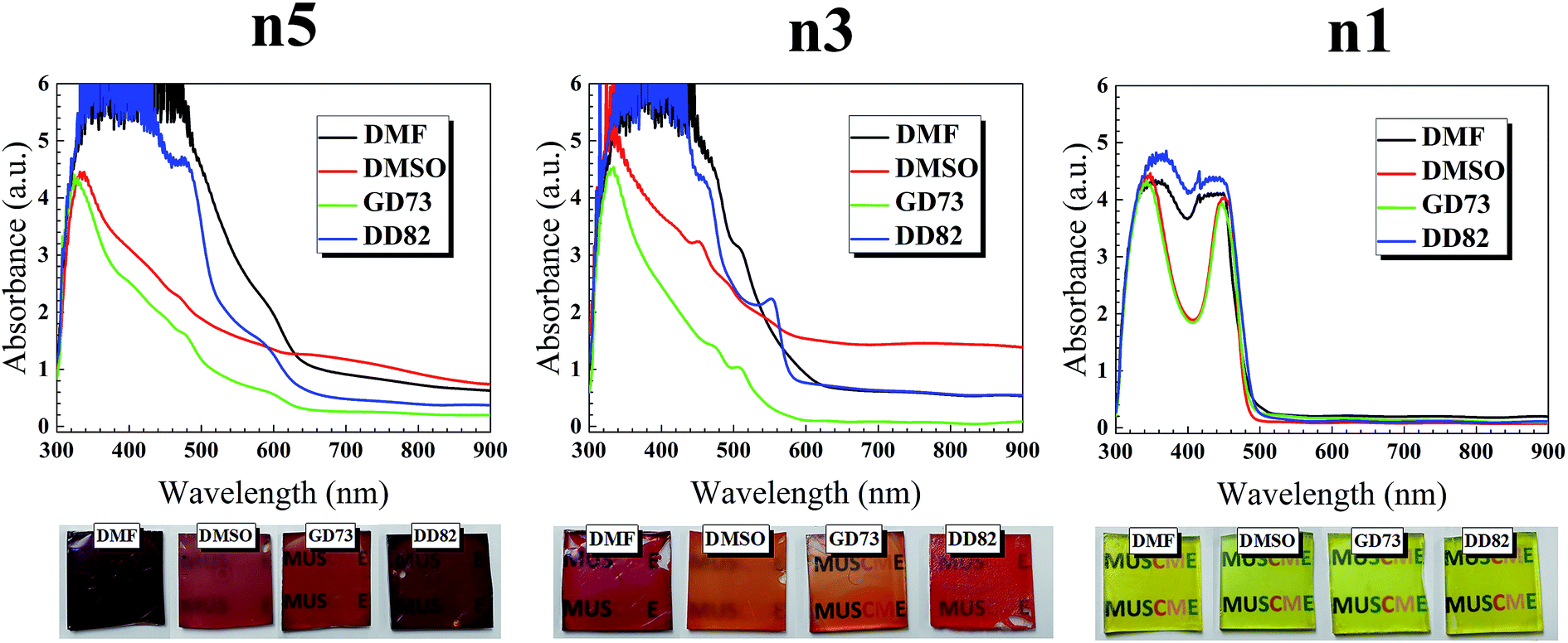 | ||
| Fig. 1 UV-vis absorption spectra and film images of (PEA)2(MA)n−1PbnIn+1Br2n perovskite films (n1, n3 and n5). | ||
Fig. 2 compares the surface morphology among the solvent types. Perovskites n1, n3 and n5 from DMF showed cracks and pinholes due to rapid crystallization, while n1, n3 and n5 from DMSO and GD73 tended to have wrinkle features and low crystallinity (as identified by XRD results in Fig. 3a). The wrinkling arose from the isotropic compressive stress during the formation of intermediate phases and relaxation and due to a minimum total energy.45,46 Overall, the low dimensional perovskites from DD82 possessed smoother and denser morphologies with higher crystallinity, properties necessary for high performance optoelectronics.
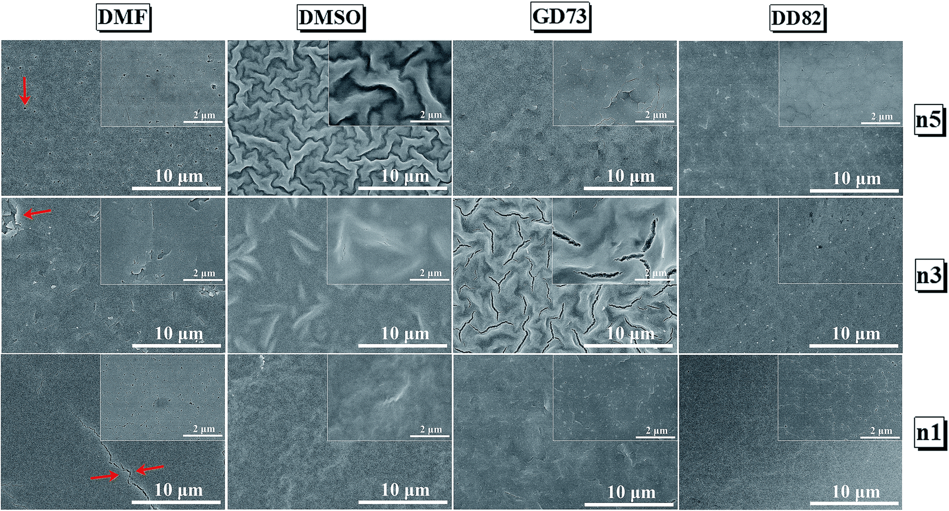 | ||
| Fig. 2 SEM images of (PEA)2(MA)n−1PbnIn+1 Br2n perovskite thin films from different solvent types; DMF, DMSO, GBL:DMSO = 7:3, and DMF:DMSO = 8:2. | ||
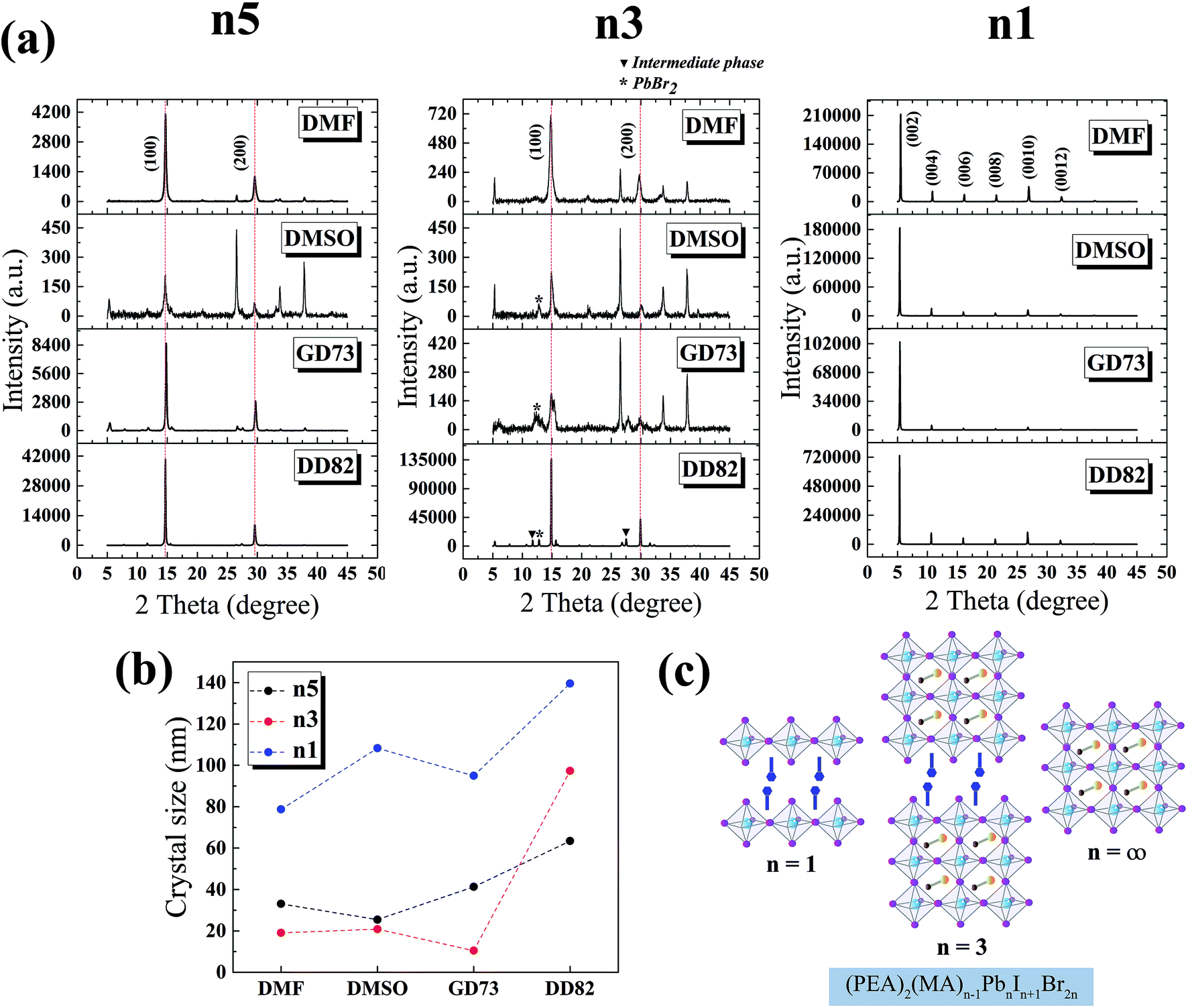 | ||
| Fig. 3 (a) X-ray diffraction spectra of n5, n3 and n1 perovskite thin films from different solvents; (b) crystallite size of (PEA)2(MA)n−1PbnIn+1Br2n perovskite from different solvents; and (c) (PEA)2(MA)n−1PbnIn+1Br2n perovskite structures where n = 1, 3 and 5. | ||
3.2 Solvent effects on crystallinity
The XRD patterns of MAPbI3 perovskite phases have been reported at 14.1°, 28.4°, 31.9° and 43.2° corresponding to the (110), (220), (310) and (330) planes.47 The replacement of Br slightly shifted the diffraction angles and changed the crystal structure from tetragonal (110) to pseudocubic (100).9,48 Fig. 3a shows the XRD results of n5/DD82 perovskite; 14.7° and 29.6° corresponded to the (100) and (200) planes, respectively. For the n3 perovskite, the diffraction peaks located at 14.9° and 29.9° indicated the (h00) planes of 3D perovskite phase and the peaks at 26.5°, 33.8° and 37.8° corresponded to the (00l) plane of (PEA)2PbI2Br2. Moreover, the PbBr2 residues were found at 12.8°; intermediate phases were ascribed by the peaks at 11.7° and 27.5°.39 The XRD peaks of n1/DD82 are located at 5.3°, 10.6°, 16.0°, 21.3°, 26.7° and 32.2°, which corresponded to (002), (004), (006), (008), (0010) and (0012) planes, respectively.49,50 With DD82 usage, XRD peaks for n1, n3, and n5 were greatly enhanced when compared with the peaks from the other solvents; this was consistent with the better morphology that was observed in Fig. 2. Through Scherrer equation, crystallite sizes were calculated, showing bigger gain sizes for all low dimensional systems when DD82 was used as the solvent as shown in Fig. 3b.3.3 Solvent effects on electronic properties
The charge separation mechanisms along with tail defect states were explored by the SPV technique. The SPV spectra exhibit an in-phase (X) and a phase-shifted by 90° signals (Y) according to the chopped light signal, and related to fast and slow responses respectively. The SPV signals of low dimensional perovskites dissolved in DMF, DMSO, GD73, and DD82 are summarized in Fig. 4. Through the charge potential difference (CPD),51,52 the n5 and n3 perovskites were determined to be p-type semiconductors, which could be identified by the negative SPV signals where photo-generated electron carriers were preferentially separated into the external interface, whereas the holes moved towards the bulk.53 Intrinsic p-type doping was induced by the presence of lead vacancies (VPb), whereas n-type doping resulted from the presence of iodide vacancies (VI) seen in PbI2 rich films.54–57 For n1, most of the solvents led to the n-type, thereby signaling incomplete conversion (excess PbI2 and deficiency of MA+ and I−). However, DD82 was a suitable solvent with an appropriate Gutmann's donor number and a decent dielectric constant, which yielded an acceptable solubility and a good interaction with Pb2+, resulting in more complete perovskite structure.18 This explained the n-type to p-type transition for n1 on using DD82 and further exemplified the benefits of DD82. The onset energy of perovskites (Eonset) was observed in the range of 2.00–2.09 eV for n5, with values increasing with decreasing dimension: 2.11–2.22 eV for n3 and 2.48–2.51 eV for n1. The onset energy, which was determined from SPV signals as shown in Fig. S3,† further supported the electronic band gap from absorption spectra as an incorporation of organic ammonium cations on perovskite causes the spatial quantum confinement via van der Waals interactions.14,58 The Tauc plot was used to determine the optical bandgap (Eg) of perovskite thin films as shown in Fig. S4.† All of the perovskites prepared in different types of solvents except n5/DMSO and n3/DMSO clearly presented a direct band gap, which only had one jump at the absorption edge and not a gradual increase followed by a jump that is typically observed for an indirect semiconductor. In the case of the indirect transition, the Urbach tail was presented just below the direct bandgap of the perovskite from a relativistic spin–orbit splitting of the lower conduction band.59 As shown in Fig. 5 and S5,† Eg and Eonset are slightly shifted towards each other as Eonset is initiated from the separation of photon-excited charge carriers, which could be trapping or de-trapping at defect states to a localized unoccupied state, while Eg is the excitation from a localized occupied state to a localized unoccupied state.30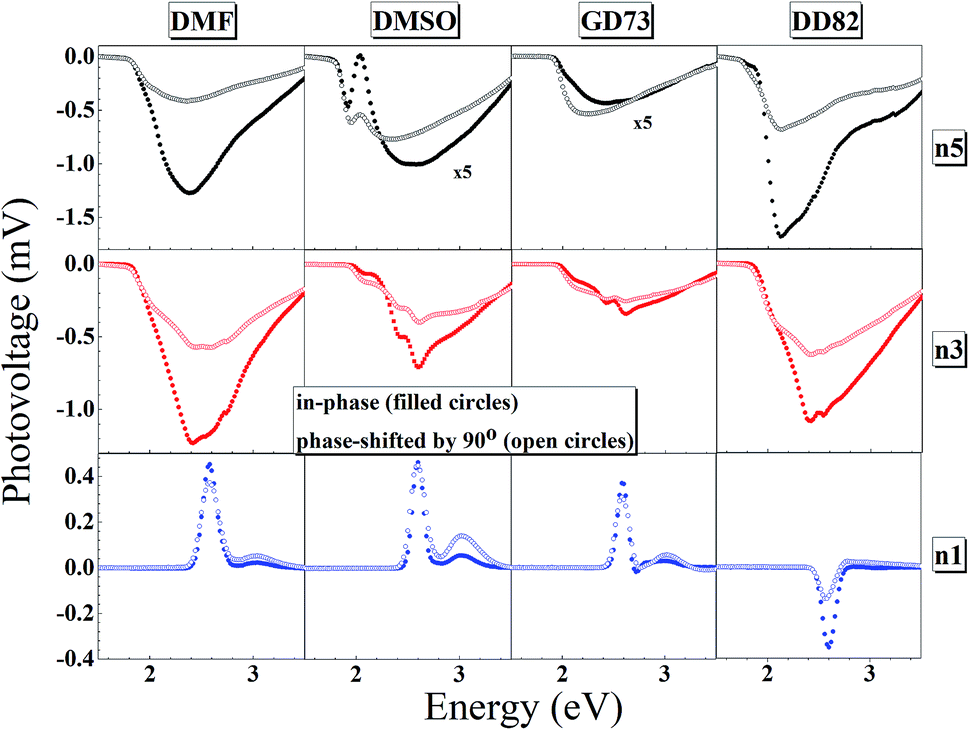 | ||
| Fig. 4 In-phase and phase-shifted by 90° overview of the surface photovoltage spectra for n5, n3 and n1 Br–I perovskite thin films. | ||
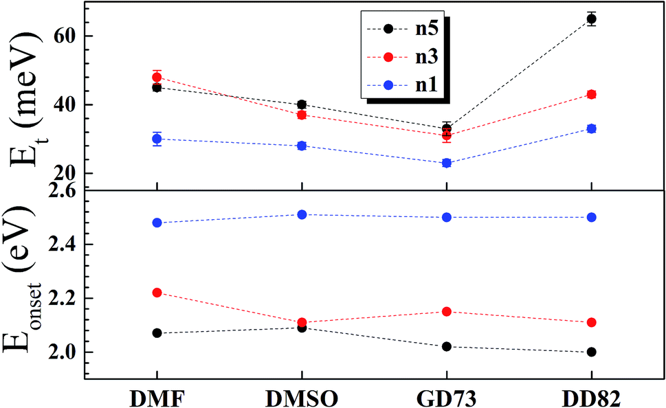 | ||
| Fig. 5 Energy tail states and onset energy for n5, n3 and n1 Br–I perovskite thin films. | ||
The high SPV signals from DD82 and DMF solvents represented the strong charge separation ability, which indicated better exciton generation upon light excitation. Shallow defects like dangling bond or dislocation at the surface could also be observed by fitting SPV as described in previous works.24,30,60 GD73 had the lowest tail defects and DD82 had the highest tail defects. However, unlike deep defects, tail defects were commonly presented in the perovskite and did not significantly impact diffusion length and solar performance.55 To mitigate tail defects of DD82, previously developed sequential method like repeated cation doping24 could be beneficial.
To further understand the defects beyond surface, time resolved photoluminescence (TRPL) was performed to probe inside perovskite films. In our experiments on perovskite/glass slide, the PL decay of perovskite exhibited a tri-exponential behavior having slowest decay (τ1), medium decay (τ2), and fastest decay (τ3).61 Medium component (τ2) and fast component (τ3) were usually associated with Shockley–Read–Hall (SRH) recombination and intrinsic electron–hole recombination, respectively, whereas the slow component (τ1) was linked to free electron–hole recombination.62 As shown in Fig. 6 and Table 2, DD82-based and DMSO-based perovskites reveal the longest average time decays, which indicate the lower overall deep defects. In the 3D system, DMSO as a solvent was linked to lower defects.20–22 In case of n5/DMSO and n3/DMSO, the formation of wrinkles only occurred on the surface and not in the bulk of the material from the release of compressive stress during perovskite crystallization, which explained why those films still exhibited longer decay lifetime despite poor surfaces.63 Time decays were longer with higher dimensions of the same solvent type due to weaker electron–hole binding energy and therefore less recombination.64 Moreover, DD82 perovskite exhibited longer τ1 and more τ1 weights (A1), which indicated a decrease in the intrinsic electron–hole radiative recombination and an increase in the free electron–hole recombination, which made them superior for photovoltaic application, consistent with more charge separation from SPV results. DD82 allowed perovskites to form larger grain size in which defects were lower and hence increased their fluorescence lifetime.
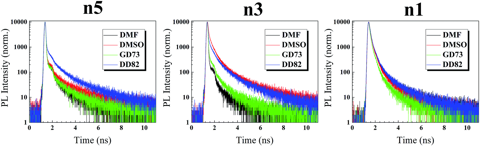 | ||
| Fig. 6 Time-resolved photoluminescence of (PEA)2(MA)n−1PbnIn+1Br2n perovskite films. | ||
| τ1 (ns) | τ2 (ns) | τ3 (ns) | A1 | A2 | A3 | χ2 | τaverage (ns) | |
|---|---|---|---|---|---|---|---|---|
| (PEA)2(MA)4Pb5I6Br10 | ||||||||
| DMF | 15.85 | 3.65 | 0.0323 | 3.02 | 4.83 | 92.15 | 1.20 | 12.02 |
| DMSO | 22.34 | 4.42 | 0.0335 | 5.31 | 5.52 | 89.17 | 1.28 | 18.89 |
| GBL:DMSO (7:3) |
15.52 | 2.88 | 0.0372 | 4.32 | 4.51 | 91.18 | 1.24 | 12.92 |
| DMF:DMSO (8:2) |
20.35 | 4.15 | 0.0571 | 14.17 | 15.80 | 70.03 | 1.24 | 17.16 |
|
||||||||
| (PEA)2(MA)2Pb3I4Br6 | ||||||||
| DMF | 12.21 | 3.13 | 0.042 | 1.69 | 3.27 | 95.04 | 1.08 | 8.15 |
| DMSO | 20.27 | 3.49 | 0.377 | 16.61 | 42.81 | 40.58 | 1.89 | 14.66 |
| GBL:DMSO (7:3) |
13.07 | 2.97 | 0.045 | 4.53 | 7.69 | 87.77 | 1.16 | 9.79 |
| DMF:DMSO (8:2) |
16.79 | 3.51 | 0.142 | 18.02 | 27.68 | 54.30 | 1.41 | 13.31 |
|
||||||||
| (PEA)2PbI2Br2 | ||||||||
| DMF | 17.14 | 2.99 | 0.858 | 7.11 | 40.54 | 52.35 | 1.54 | 8.64 |
| DMSO | 14.48 | 2.78 | 0.793 | 6.90 | 40.27 | 52.83 | 1.65 | 7.06 |
| GBL:DMSO (7:3) |
10.15 | 2.17 | 0.630 | 6.17 | 40.46 | 53.36 | 1.31 | 4.60 |
| DMF:DMSO (8:2) |
18.33 | 3.15 | 0.887 | 7.95 | 40.13 | 51.92 | 1.61 | 9.77 |
4. Conclusions
With high stability and band gap tunability, low dimensional perovskites have great potential for solution processable optoelectronics like LEDS and semi-transparent solar cells. In this work, we identified DD82 as the most suitable solvent for low dimensional, mixed halide perovskite for solar application. Having both DMF and DMSO, DD82 struck the right balance for the crystal formation to achieve a good surface morphology, a large crystallite size, and a good charge separation while retaining the low defect typical of DMSO-based system.Conflicts of interest
There are no conflicts of interest to declare.Acknowledgements
This work was mainly supported by the EGAT and NSTDA (funding no. FDA-CO-2560-5449-TH). We would like to acknowledge the Center of Excellence for Innovation in Chemistry (PERCH-CIC), Faculty of Science, Mahidol University, the Thailand Research Fund (MRG61 – Pongsakorn Kanjanaboos), the Research Fund for DPST graduate with First Placement (#005/2558) (The Institute for Promotion of Teaching Science and Technology), and Dr Supavadee Kiatisevi for fruitful discussions.References
- D. B. Mitzi, K. Chondroudis and C. R. Kagan, Inorg. Chem., 1999, 38, 6246–6256 CrossRef CAS.
- G. Xing, N. Mathews, S. Sun, S. S. Lim, Y. M. Lam, M. Grätzel, S. Mhaisalkar and T. C. Sum, Science, 2013, 342, 344–347 CrossRef CAS PubMed.
- Z. Xiao, C. Bi, Y. Shao, Q. Dong, Q. Wang, Y. Yuan, C. Wang, Y. Gao and J. Huang, Energy Environ. Sci., 2014, 7, 2619–2623 RSC.
- J. Chen and N. G. Park, J. Phys. Chem. C, 2018, 122, 14039–14063 CrossRef CAS.
- N. J. Jeon, H. Na, E. H. Jung, T.-Y. Yang, Y. G. Lee, G. Kim, H.-W. Shin, S. Il Seok, J. Lee and J. Seo, Nat. Energy, 2018, 3, 682–689 CrossRef CAS.
- NREL, https://www.nrel.gov/pv/assets/pdfs/pv-efficiency-chart.20181221.pdf, accessed 02 January 2019.
- H. J. Snaith, J. Phys. Chem. Lett., 2013, 4, 3623–3630 CrossRef CAS.
- T. Baikie, Y. Fang, J. M. Kadro, M. Schreyer, F. Wei, S. G. Mhaisalkar, M. Graetzel and T. J. White, J. Mater. Chem. A, 2013, 1, 5628–5641 RSC.
- D. Cui, Z. Yang, D. Yang, X. Ren, Y. Liu, Q. Wei, H. Fan, J. Zeng and S. Liu, J. Phys. Chem. C, 2016, 120, 42–47 CrossRef CAS.
- W. J. Yin, Y. Yan and S. H. Wei, J. Phys. Chem. Lett., 2014, 5, 3625–3631 CrossRef CAS PubMed.
- Y. Tu, J. Wu, Z. Lan, X. He, J. Dong, J. Jia, P. Guo, J. Lin, M. Huang and Y. Huang, Sci. Rep., 2017, 7, 44603 CrossRef CAS PubMed.
- M. Yang, T. Zhang, P. Schulz, Z. Li, G. Li, D. H. Kim, N. Guo, J. J. Berry, K. Zhu and Y. Zhao, Nat. Commun., 2016, 7, 2–10 Search PubMed.
- P. Kaewurai, J. Ponchai, K. Amratisha, A. Naikaew, K. Z. Swe, K. Pinsuwan, C. Boonthum, S. Sahasithiwat and P. Kanjanaboos, Appl. Phys. Express, 2018, 12, 15506 CrossRef.
- L. N. Quan, M. Yuan, R. Comin, O. Voznyy, E. M. Beauregard, S. Hoogland, A. Buin, A. R. Kirmani, K. Zhao, A. Amassian, D. H. Kim and E. H. Sargent, J. Am. Chem. Soc., 2016, 138, 2649–2655 CrossRef CAS PubMed.
- J. Calabrese, N. L. Jones, R. L. Harlow, N. Herron, D. L. Thorn and Y. Wang, J. Am. Chem. Soc., 1991, 113, 2328–2330 CrossRef CAS.
- D. H. Cao, C. C. Stoumpos, O. K. Farha, J. T. Hupp and M. G. Kanatzidis, J. Am. Chem. Soc., 2015, 137, 7843–7850 CrossRef CAS PubMed.
- R. L. Milot, R. J. Sutton, G. E. Eperon, A. A. Haghighirad, J. Martinez Hardigree, L. Miranda, H. J. Snaith, M. B. Johnston and L. M. Herz, Nano Lett., 2016, 16, 7001–7007 CrossRef CAS PubMed.
- J. C. Hamill, J. Schwartz and Y.-L. Loo, ACS Energy Lett., 2018, 3, 92–97 CrossRef CAS.
- N. Ahn, D. Y. Son, I. H. Jang, S. M. Kang, M. Choi and N. G. Park, J. Am. Chem. Soc., 2015, 137, 8696–8699 CrossRef CAS PubMed.
- J. H. Heo, D. H. Song, H. J. Han, S. Y. Kim, J. H. Kim, D. Kim, H. W. Shin, T. K. Ahn, C. Wolf, T.-W. Lee and S. H. Im, Adv. Mater., 2015, 27, 3424–3430 CrossRef CAS PubMed.
- D. Kiermasch, P. Rieder, K. Tvingstedt, A. Baumann and V. Dyakonov, Sci. Rep., 2016, 6, 1–7 CrossRef PubMed.
- G. W. P. Adhyaksa, L. W. Veldhuizen, Y. Kuang, S. Brittman, R. E. I. Schropp and E. C. Garnett, Chem. Mater., 2016, 28, 5259–5263 CrossRef CAS.
- N. J. Jeon, J. H. Noh, Y. C. Kim, W. S. Yang, S. Ryu and S. Il Seok, Nat. Mater., 2014, 13, 897–903 CrossRef CAS PubMed.
- C. Boonthum, K. Pinsuwan, J. Ponchai, T. Srikhirin and P. Kanjanaboos, Appl. Phys. Express, 2018, 11, 065503 CrossRef.
- M. Yin, F. Xie, H. Chen, X. Yang, F. Ye, E. Bi, Y. Wu, M. Cai and L. Han, J. Mater. Chem. A, 2016, 4, 8548–8553 RSC.
- T. Bu, L. Wu, X. Liu, X. Yang, P. Zhou, X. Yu, T. Qin, J. Shi, S. Wang, S. Li, Z. Ku, Y. Peng, F. Huang, Q. Meng, Y.-B. Cheng and J. Zhong, Adv. Energy Mater., 2017, 7, 1700576 CrossRef.
- L. Kronik and Y. Shapira, Surf. Interface Anal., 2001, 31, 954–965 CrossRef CAS.
- T. Dittrich, C. Awino, P. Prajongtat, B. Rech and M. C. Lux-Steiner, J. Phys. Chem. C, 2015, 119, 23968–23972 CrossRef CAS.
- V. Donchev, T. Ivanov, K. Germanova and K. Kirilov, Trends Appl. Spectrosc., 2010, 8, 27–66 CAS.
- N. Henjongchom, N. Rujisamphan, I. M. Tang and T. Supasai, Phys. Status Solidi A, 2018, 215, 1–8 CrossRef.
- V. Pokorný, V. Štejfa, M. Fulem, C. Červinka and K. Růžička, J. Chem. Eng. Data, 2017, 62, 4174–4186 CrossRef.
- A. J. C. Bunkan, J. Hetzler, T. Mikoviny, A. Wisthaler, C. J. Nielsen and M. Olzmann, Phys. Chem. Chem. Phys., 2015, 17, 7046–7059 RSC.
- M. Fulem, K. Růžička and M. Růžička, Fluid Phase Equilib., 2011, 303, 205–216 CrossRef CAS.
- S. Lin, W. Li, H. Sun, W. Xu, W. Guo, M. Xia and K. Yang, MATEC Web Conf., 2015, 22, 5002 CrossRef.
- P. H. Huang, Y. H. Wang, J. C. Ke and C. J. Huang, Energies, 2017, 10, 1–8 CAS.
- F. Wang, S. Bai, W. Tress, A. Hagfeldt and F. Gao, npj Flexible Electronics, 2018, 2, 22 CrossRef.
- F. Wang, H. Yu, H. Xu and N. Zhao, Adv. Funct. Mater., 2015, 25, 1120–1126 CrossRef CAS.
- W. S. Yang, J. H. Noh, N. J. Jeon, Y. C. Kim, S. Ryu, J. Seo and S. I. Seok, Science, 2015, 348, 1234–1237 CrossRef CAS PubMed.
- X. Guo, C. McCleese, C. Kolodziej, A. C. S. Samia, Y. Zhao and C. Burda, Dalton Trans., 2016, 45, 3806–3813 RSC.
- B. Cai, W.-H. Zhang and J. Qiu, Chin. J. Catal., 2015, 36, 1183–1190 CrossRef CAS.
- M. Shahiduzzaman, K. Yamamoto, Y. Furumoto, K. Yonezawa, K. Hamada, K. Kuroda, K. Ninomiya, M. Karakawa, T. Kuwabara, K. Takahashi, K. Takahashi and T. Taima, Org. Electron., 2017, 48, 147–153 CrossRef CAS.
- M.-R. Ahmadian-Yazdi, A. Rahimzadeh, Z. Chouqi, Y. Miao and M. Eslamian, AIP Adv., 2018, 8, 25109 CrossRef.
- M. Habibi, A. Rahimzadeh and M. Eslamian, Eur. Phys. J. E, 2016, 39, 30 CrossRef PubMed.
- M. Habibi, A. Rahimzadeh, I. Bennouna and M. Eslamian, Coatings, 2017, 7, 42 CrossRef.
- G. Nasti, S. Sanchez, I. Gunkel, S. Balog, B. Roose, B. D. Wilts, J. Teuscher, G. Gentile, P. Cerruti, V. Ambrogi, C. Carfagna, U. Steiner and A. Abate, Soft Matter, 2017, 13, 1654–1659 RSC.
- K. A. Bush, N. Rolston, A. Gold-Parker, S. Manzoor, J. Hausele, Z. J. Yu, J. A. Raiford, R. Cheacharoen, Z. C. Holman, M. F. Toney, R. H. Dauskardt and M. D. McGehee, ACS Energy Lett., 2018, 3, 1225–1232 CrossRef CAS.
- R. Sedighi, F. Tajabadi, S. Shahbazi, S. Gholipour and N. Taghavinia, ChemPhysChem, 2016, 17, 2382–2388 CrossRef CAS PubMed.
- Y. Zhao, A. M. Nardes and K. Zhu, Faraday Discuss., 2014, 176, 301–312 RSC.
- N. Kitazawa, Mater. Sci. Eng., B, 1997, 49, 233–238 CrossRef.
- D. Liang, Y. Peng, Y. Fu, M. J. Shearer, J. Zhang, J. Zhai, Y. Zhang, R. J. Hamers, T. L. Andrew and S. Jin, ACS Nano, 2016, 10, 6897–6904 CrossRef CAS PubMed.
- T. Dittrich, O. Garcia Vera, S. Fengler, S. Pineda and S. Bönisch, Rev. Sci. Instrum., 2019, 90, 26102 CrossRef PubMed.
- T. Dittrich, https://www.helmholtz-berlin.de/media/media/forschung/energie/heterogen/eta/methods/spv-techniques-2010-08-09.pdf, accessed 09 August 2010.
- L. Barnea-Nehoshtan, S. Kirmayer, E. Edri, G. Hodes and D. Cahen, J. Phys. Chem. Lett., 2014, 5, 2408–2413 CrossRef CAS PubMed.
- Q. Wang, Y. Shao, H. Xie, L. Lyu, X. Liu, Y. Gao and J. Huang, Appl. Phys. Lett., 2014, 105, 163508 CrossRef.
- W.-J. Yin, T. Shi and Y. Yan, Appl. Phys. Lett., 2014, 104, 63903 CrossRef.
- L. A. Frolova, N. N. Dremova and P. A. Troshin, Chem. Commun., 2015, 51, 14917–14920 RSC.
- A. Naikaew, P. Prajongtat, M. C. Lux-Steiner, M. Arunchaiya and T. Dittrich, Appl. Phys. Lett., 2015, 106, 232104 CrossRef.
- X. Gan, O. Wang, K. Liu, X. Du, L. Guo and H. Liu, Sol. Energy Mater. Sol. Cells, 2017, 162, 93–102 CrossRef CAS.
- T. Wang, B. Daiber, J. M. Frost, S. A. Mann, E. C. Garnett, A. Walsh and B. Ehrler, Energy Environ. Sci., 2017, 10, 509–515 RSC.
- A. Owino Juma, A. Azarpira, A. Steigert, M. Pomaska, C. H. Fischer, I. Lauermann and T. Dittrich, J. Appl. Phys., 2013, 114, 1–7 CrossRef.
- J. Byun, H. Cho, C. Wolf, M. Jang, A. Sadhanala, R. H. Friend, H. Yang and T.-W. Lee, Adv. Mater., 2016, 28, 7515–7520 CrossRef CAS PubMed.
- Y. Jiang, X. Wen, A. Benda, R. Sheng, A. W. Y. Ho-Baillie, S. Huang, F. Huang, Y. B. Cheng and M. A. Green, Sol. Energy Mater. Sol. Cells, 2016, 151, 102–112 CrossRef CAS.
- S. Braunger, L. E. Mundt, C. M. Wolff, M. Mews, C. Rehermann, M. Jošt, A. Tejada, D. Eisenhauer, C. Becker, J. A. Guerra, E. Unger, L. Korte, D. Neher, M. C. Schubert, B. Rech and S. Albrecht, J. Phys. Chem. C, 2018, 122, 17123–17135 CrossRef CAS.
- J. Wang, J. Leng, J. Liu, S. He, Y. Wang, K. Wu and S. Jin, J. Phys. Chem. C, 2017, 121, 21281–21289 CrossRef CAS.
- J. H. Noh, S. H. Im, J. H. Heo, T. N. Mandal and S. Il Seok, Nano Lett., 2013, 13, 1764–1769 CrossRef CAS PubMed.
Footnote |
| † Electronic supplementary information (ESI) available. See DOI: 10.1039/c9ra00971j |
| This journal is © The Royal Society of Chemistry 2019 |