DOI:
10.1039/C9RA00586B
(Paper)
RSC Adv., 2019,
9, 12394-12403
Bilayer MSe2 (M = Zr, Hf) as promising two-dimensional thermoelectric materials: a first-principles study
Received
23rd January 2019
, Accepted 7th April 2019
First published on 23rd April 2019
Abstract
Motivated by the experimental synthesis of two-dimensional MSe2 (M = Zr, Hf) thin films, we set out to investigate the electronic, thermal, and thermoelectric transport properties of 1T-phase MSe2 (M = Zr, Hf) bilayers on the basis of first-principles calculations and Boltzmann transport theory. Both bilayer ZrSe2 and HfSe2 are indirect band gap semiconductors possessing degenerate conduction bands and stair-like-shaped DOS, which provide a high n-doped power factor. In combination with the low lattice thermal conductivity that originated from the low phonon frequency of acoustic modes and the coupling of acoustic modes with optical modes, the maximum figure of merits ZT at room temperature for n-type doping are predicted as 1.84 and 3.83 for ZrSe2 and HfSe2 bilayers, respectively. Our results suggest that bilayer conformation of ZrSe2 and HfSe2 are promising thermoelectric materials with superior performance to their bulk counterparts.
1 Introduction
Considering the widespread use of the thermoelectric generators, researchers have been in pursuit of highly efficient thermoelectric (TE) materials over the past few decades. The efficiency of a thermoelectric material is quantified by the dimensionless figure of merit ZT = S2σT/(κe + κl), where S, σ, T, and (κe + κl) are the Seebeck coefficient, electrical conductivity, absolute temperature, and total thermal conductivity contributed by the electrons and phonons, respectively. The power factor (PF = S2σ) is used to assess the electronic transport performance of a TE material. Different strategies such as increasing the PF through optimal doping and band engineering1–5 or reducing κl by nanostructural engineering6,7 have been proposed to improve the TE performance. Among the various TE materials, two-dimensional (2D) materials, especially transition metal di-chalcogenides (TMDCs) MX2 (M = Mo, W; X = S, Se), have attracted more attention due to their unique properties which are superior to those of their bulk counterparts for thermoelectric applications. It is well known that, depending on the arrangement of the atoms, the structures of 2D TMDCs can be mainly categorized as two different crystal structures, trigonal prismatic (hexagonal, 2H-MoS2-type) or octahedral (tetragonal, 1T-CdI2-type). The difference is that the anion hexagonal nets are A⋯A stacked in MoS2, while they are A⋯B stacked in 1T-CdI2.8 However, as typical 2H-TMDCs, monolayer MoS2 and WSe2 exhibit unsatisfactory ZT values of 0.1 and 0.7 at high temperature,9,10 due to the high lattice thermal conductivity in these 2H-MoS2 (symmetry group P![[6 with combining macron]](https://www.rsc.org/images/entities/char_0036_0304.gif) m2) based crystal structures. Recently, in contrast, the trigonal 1T-CdI2 (symmetry group P
m2) based crystal structures. Recently, in contrast, the trigonal 1T-CdI2 (symmetry group P![[3 with combining macron]](https://www.rsc.org/images/entities/char_0033_0304.gif) m1) type TMDCs, e.g. MX2 (M = Zr, Hf, and X = S, Se) have emerged as competitive materials for thermoelectric applications due to their outstanding properties such as the quite low lattice thermal conductivity. Yumnam et al. confirmed that the κl of bulk Zr and Hf based TMDCs is almost 15 times lower than those of W and Mo based TMDCs.11 Ding et al. reported the low lattice thermal conductivity and promising figure of merit of monolayer MSe2.12 Consequently, monolayer 1T-CdI2 TMDCs exhibits better thermoelectric performance as compared to 2H-MoS2 types. Recent studies have also focused on further improving the ZT of monolayer 1T-type TMDCs through strain engineering.13–15
m1) type TMDCs, e.g. MX2 (M = Zr, Hf, and X = S, Se) have emerged as competitive materials for thermoelectric applications due to their outstanding properties such as the quite low lattice thermal conductivity. Yumnam et al. confirmed that the κl of bulk Zr and Hf based TMDCs is almost 15 times lower than those of W and Mo based TMDCs.11 Ding et al. reported the low lattice thermal conductivity and promising figure of merit of monolayer MSe2.12 Consequently, monolayer 1T-CdI2 TMDCs exhibits better thermoelectric performance as compared to 2H-MoS2 types. Recent studies have also focused on further improving the ZT of monolayer 1T-type TMDCs through strain engineering.13–15
It is known that the number of atomic layers has a significant influence on the band structure, phonon spectrum and other properties of 2D materials. For example, reducing the thickness of the 1H-MX2 (M = Mo, W; X = S, Se, Te) systematically from bulk to the monolayer limit causes a blue shift in the band gap energies, together leading to tunability in the electronic band gap and transitions from indirect to direct bands.16 Currently, further theoretical studies concerning the TMDCs bilayers have been reported, such as the variation of thermoelectric performance by electric fields in bilayer MX2 (M = W, Mo; X = S, Se)17 and the metallization in the phase-engineered ZrX2 (X = S, Se, Te) induced by pressure and electric fields.18 Generally, by turning the atomic layers of 2D 1T-CdI2 TMDCs, it is feasible to further optimize the thermoelectric performance. However, to the best of our knowledge, previous studies on the thermal and electronic transport properties of the 1T-type phase MSe2 (M = Zr, Se) bilayers have been rarely reported to date. Thus, we set out to perform a systematic investigation on the thermoelectric performance of 2D ZrSe2 and HfSe2 bilayers.
In the following, we present the electronic structure and thermoelectric properties of 1T-phase MSe2 (M = Zr, Hf) bilayers employing first-principles calculations combined with Boltzmann transport theory with van der Waals correction, on-site Coulomb and exchange interactions included. The electronic structure of these bilayer MSe2 exhibit a conduction band degeneracy and stair-like-shape density of state, which is absent in the bulk counterparts or monolayer. Such unique band features of bilayer ZrSe2 and HfSe2 contribute to the high power factor. Furthermore, the phonon dispersion of these materials display a small allowed acoustic frequency (3.48–3.93 THz), resulting in a low lattice thermal conductivity. Our theoretical findings demonstrate that the 1T-phase of 2D ZrSe2 and HfSe2 bilayers are promising candidates for thermoelectric applications. And we hope that our work will provide useful information for further experimental and theoretical studies for optimizing the thermoelectric performance of multilayer TE materials.
2 Computational details
2.1 DFT calculation
In the present work, the structure optimization and electronic structure calculations were performed by using the projector-augmented wave (PAW) method,19 as implemented in the Vienna ab initio simulation package (VASP) code.20–22 The electron exchange-correlation functional are treated using a generalized gradient approximation (GGA) in the form proposed by Perdew, Burke, and Ernzerhof (PBE)23 coupled with the DFT-D3 method of Grimme to assess the effect of van der Waals (vdW) interactions.24 Moreover, the DFT + U method is used for the corrections of on-site coulomb interactions with the effective Hubbard U of 5.0 eV to act on the Zr 4d and Hf 5d states, which can greatly improve the quality of PBE and give the correct electronic structure. We selected a value of 5.0 eV for the effective Hubbard U after reference to previous studies.18,25–27 The lattice parameters and atomic coordinates were optimized until all of the forces were less than 0.005 eV Å−1 per atom. The relaxation of energy is taken as 1.0 × 10⁻⁶ eV. The plane-wave basis cut-off was 400 eV and a Monkhorst–Pack mesh was set to 21 × 21 × 1 for the Brillouin zone integration, which was sufficient for energy convergence and static calculations. The spin–orbit coupling (SOC) has been taken into account, since it has been proven to play an important effect on the band structure and power factor calculations of many TE materials.11,28–30 The calculated equilibrium lattice parameters are in good agreement with available reports as shown in Table 1.
Table 1 A comparison of the calculated lattice constant and bandgap results for bilayer MSe2 with the available results of bulk and monolayer forms of the same system
| Forms |
Material |
a (Å) |
c (Å) |
Eg (eV) |
| Bilayer |
ZrSe2 |
3.85 |
|
0.99 |
| HfSe2 |
3.80 |
|
1.07 |
| Bulk31 |
ZrSe2 |
3.76 |
6.15 |
|
| HfSe2 |
3.733 |
6.146 |
1.13 |
| Monolayer32 |
ZrSe2 |
3.80 |
|
1.54 |
| HfSe2 |
3.76 |
|
1.39 |
2.2 Electronic transport property calculation
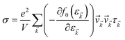
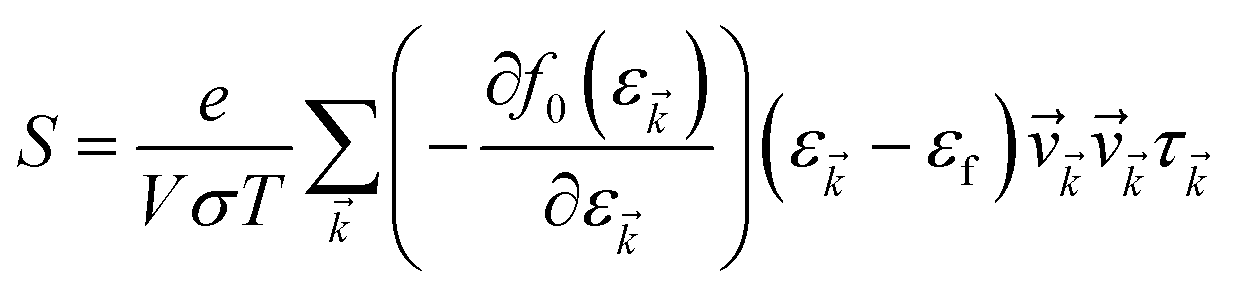
The accurate calculation of the electronic structure is the premise for obtaining accurate transport properties, so we use the more dense 47 × 47 × 1 k-points Monkhorst–Pack mesh in these calculations. On the basis of the band structure obtained from VASP, the electronic transport properties, including S, σ/τ, and κe/τ are calculated by solving the Boltzmann transport equation (BTE) within the rigid band approximation (RBA)33–35 and constant scattering time (τ) approximation (CSTA) as implemented in the BoltzTraP package.36 In terms of the Fermi–Dirac distribution function
f0(ε![[k with combining right harpoon above (vector)]](https://www.rsc.org/images/entities/i_char_006b_20d1.gif) ) = 1/[exp((ε − εf)/kBT) + 1] ) = 1/[exp((ε − εf)/kBT) + 1] |
the TE transport coefficients can be expressed as| |
 | (1) |
| |
 | (2) |
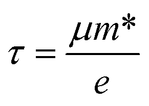
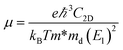
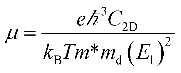
where ℏ, kB and T are the reduced Planck constant, the Boltzmann constant and the temperature, respectively; εf and ε are the Fermi energy and the k-point band energy, respectively; V is the volume of the unit cell; ![[v with combining right harpoon above (vector)]](https://www.rsc.org/images/entities/i_char_0076_20d1.gif) = (1/ℏ)∇ε is the group velocity, which can be obtained from the first-principles band structure calculations; τ is the relaxation time. Clearly, a knowledge of τ is required to obtain the value of the electrical conductivity, σ. Usually, the relaxation time, τ is obtained from either fitting of the experiments37 or theoretical estimation. In this work, the calculation of relaxation time, τ is incorporated on the basis of the Bardeen–Shockley deformation potential (DP) theory,38 which has been proven to be a robust strategy to predict the mobility of 2D materials in previous reports and shows reliable results for known TE materials.39–44 In this approach, we consider only the longitudinal acoustic phonon scattering. From the deformation potential theory, we can derive the carrier mobility, μ on the basis of the effective-mass approximation45 as the following form
= (1/ℏ)∇ε is the group velocity, which can be obtained from the first-principles band structure calculations; τ is the relaxation time. Clearly, a knowledge of τ is required to obtain the value of the electrical conductivity, σ. Usually, the relaxation time, τ is obtained from either fitting of the experiments37 or theoretical estimation. In this work, the calculation of relaxation time, τ is incorporated on the basis of the Bardeen–Shockley deformation potential (DP) theory,38 which has been proven to be a robust strategy to predict the mobility of 2D materials in previous reports and shows reliable results for known TE materials.39–44 In this approach, we consider only the longitudinal acoustic phonon scattering. From the deformation potential theory, we can derive the carrier mobility, μ on the basis of the effective-mass approximation45 as the following form| |
 | (3) |
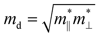
where the effective mass m* = ℏ2[∂2E()/∂2]−1 can be estimated through a quadratic fit of the energy versus k-points for the bottom (top) of the conduction (valence) band for an electron (hole). The average effective mass md is defined by  , where
  and
and  are the effective mass parallel and perpendicular to the transport direction. For the two-dimensional (2D) system, the effective elastic modulus C2D in-plane is calculated through C2D = (∂2E/∂ε2)/S0, where E, ε and S0 are, respectively, the total energy, the applied small strain (by a step of 0.5% in the present study), and the area of the investigated system. El is the deformation potential constant which can be obtained by El = dEedge/dε, where Eedge is the energy of the band edges (VBM and CBM). Finally, the estimation results on carrier mobility, μ and the effective mass, m* can be used to calculate the scattering time, τ using the following formula
| |
 | (4) |
The above DP constant and elastic constant can be calculated from first-principles calculations, while the detailed calculation methods and obtained results are shown in Section 3. In addition, the electronic contribution to thermal conductivity, κe is usually calculated via the Wiedemann–Franz law:46
where
L = 2.45 × 10
−8 W Ω K
−2 is the Sommerfeld theoretical value for free electrons. Chen and Podloucky indicated that constant Lorenz number of non-semiconductor can deviate in value by a full calculation when the Fermi level closes to the gap,
47 it should be noted that the constant Lorenz number is adopted in our calculations since the materials we studied are degenerate semiconductors.
2.3 Phonon transport property calculation
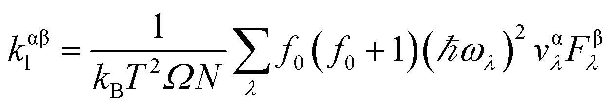
We calculate the lattice thermal conductivity by solving the phonon Boltzmann transport equation (pBTE)48 as implemented in ShengBTE.49 When considering two- and three-phonon process as the scattering sources, the linearized pBTE is written as: ![[F with combining right harpoon above (vector)]](https://www.rsc.org/images/entities/i_char_0046_20d1.gif) λ = τ0λ(λ + Δλ), where λ is the group velocity of mode λ, τ0λ is the relaxation time of mode λ, and Δλ in the dimension of velocity is a correction of the deviation to the RTA prediction. If Δλ is set to zero, the calculation is equivalent to working within the RTA. The lattice thermal conductivity can be finally calculated in terms of λ as
λ = τ0λ(λ + Δλ), where λ is the group velocity of mode λ, τ0λ is the relaxation time of mode λ, and Δλ in the dimension of velocity is a correction of the deviation to the RTA prediction. If Δλ is set to zero, the calculation is equivalent to working within the RTA. The lattice thermal conductivity can be finally calculated in terms of λ as
A full solution of pBTE requires inputs including descriptions of the harmonic and anharmonic interatomic force constants (IFCs) in the crystal structure. We employ VASP to calculate the IFCs using a well-converged 3 × 3 × 1 supercell based on the relaxed unit cell. For the anharmonic IFCs, we impose a converged cut-off distance of 0.6 nm for the atomic interactions. To obtain accurate forces, a wave function energy cut-off of 500 eV is used with an energy convergence criterion of 10−8 eV. The harmonic IFCs are obtained by Phonopy code.50 For obtaining anharmonic IFCs and for solving pBTE, we employ the ShengBTE code, based on an adaptive smearing approach to the convergence of energy51 and on an iterative solution method.52 To guarantee the convergence of lattice thermal conductivity, we impose a tested integration grid up to 41 × 41 × 1.
3 Results and discussions
3.1 Geometric structure and stability
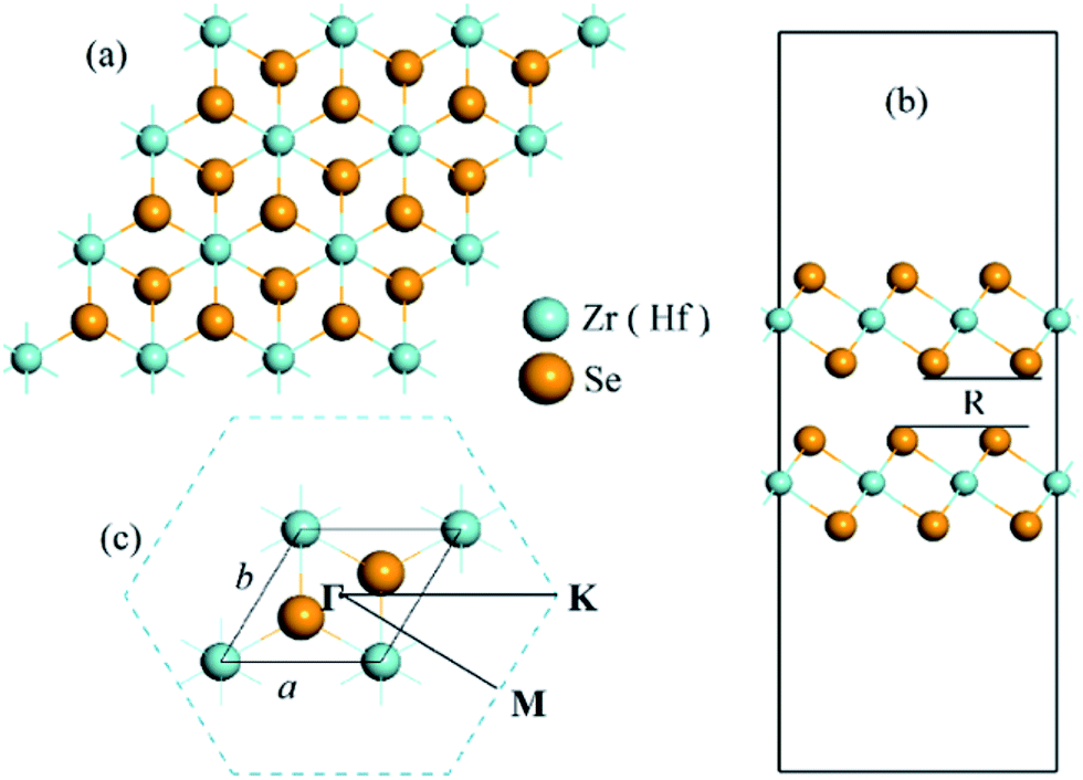
In the bulk phase, 1T-CdI2 typed ZrSe2 and HfSe2 crystallize as a layered material with tetragonal symmetry and octahedral coordination, which have strong covalent bonds for in-plane atomic layer and weak van der Waals interaction between the layers thus allowing the crystal to shear along the layered interface. It is noteworthy that the van der Waals’ correction terms are important for the accurate prediction of the structural properties of layered systems.53–55 Hence, the vdW interactions are included in all calculations in this study. In experiments, the two-dimensional TMD solids are usually obtained from their bulk phase by using micro-mechanical exfoliation,56–58 thermal laser ablation,59 chemical vapor deposition,60 vapor phase synthesis,61 or liquid exfoliation.62 And very recently there is a report of the synthesis of ZrSe2 thin films using different combinations of cation and anion precursors.63 In our calculations, the model of a bilayer structure is cut through the (0 0 1) plane of the corresponding 1T-CdI2 ZrSe2 (HfSe2) bulk crystal with a = 3.76 Å, c = 6.15 Å (a = 3.733 Å, c = 6.146 Å),31,64 and a vacuum slab about 22 Å is added in the direction perpendicular to the nano-sheet plane. The optimized lattice parameters of ZrSe2 and HfSe2 bilayers are 3.85 Å and 3.80 Å, respectively, within the GGA(PBE) + vdW + U level. We also compare the lattice parameter and bandgap of the bilayer MSe2 with their bulk and monolayer forms, as shown in Table 1. The projected top view of the bilayer is displayed in Fig. 1(a). In addition, the calculated interlayer separation of the bilayer system, R is 3.08 and 2.96 Å, for ZrSe2 and HfSe2, respectively, as shown by the side view of the bilayers in Fig. 1(b), which is in good agreement with the previous reports.18 Furthermore, phonon calculations have been performed with the finite displacement difference method as implemented in the PHONOPY package50 to confirm that bilayers of ZrSe2 and HfSe2 are dynamically stable with no imaginary frequencies.
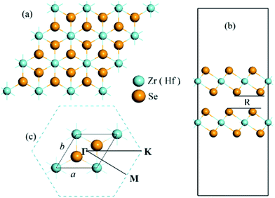 |
| | Fig. 1 (a) Top view of the ZrSe2 (HfSe2) bilayers; (b) side view of the ZrSe2 (HfSe2) bilayers with a vacuum layer about 22 Å and R is the interlayer separation; (c) the unit cell and corresponding Brillouin zone path with the high-symmetry points at Γ(0,0,0), M(0.5,0,0), K(1/3,1/3,0). The lattice parameters are denoted as a and b. The yellow and cyan represent Se and Zr (Hf) atom, respectively. | |
3.2 Electronic transport properties
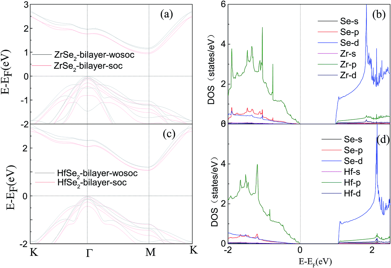
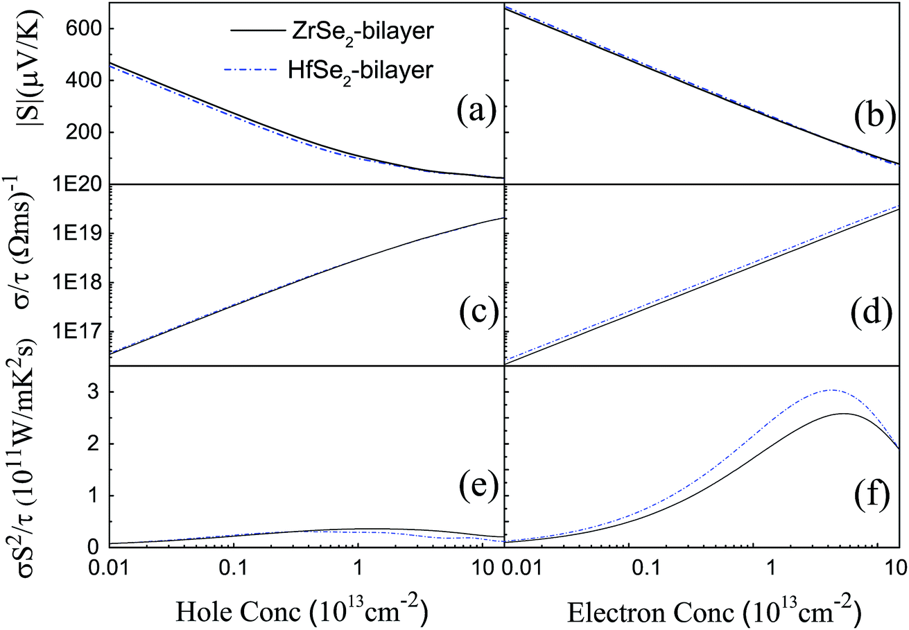
Based on the optimized structure, we calculate the electronic structure in the Brillouin zones with high symmetry k-points along K–Γ–M–K as illustrated in Fig. 1(c). We plot the band structures calculated by using GGA + U + vdW (black solid lines) and GGA + U + vdW + SOC (red solid lines) for ZrSe2 and HfSe2 bilayers, as depicted in Fig. 2(a) and (c), where the right panels of (b) and (d) are the corresponding partial density of states with SOC included. It can be seen that both ZrSe2 and HfSe2 bilayers are indirect band gap semiconductors. The valence band maximum (VBM) and conduction band minimum (CBM) are located at the Γ and M points, respectively. In addition, when SOC is included, the valence bands split at the Γ point while the conduction bands display little difference compared to the case without SOC, which indicates that there may be a non-negligible effect on the p-type properties. Therefore, the SOC has been taken into account below. The indirect band gaps in these compounds are 0.99 (ZrSe2-bilayer) and 1.07 eV (HfSe2-bilayer), which are in excellent agreement with the previous reports.18,65 From the highly precise energy band calculation, we can obtain the effective mass m* near the Fermi level, which is an important parameter of free carriers for the electronic transport. The effective mass is calculated by the formula m* = ℏ2[∂2E()/∂2]−1,66 which can be obtained by fitting the electronic bands near the Fermi level. The effective mass at the valence band maximum (hole valley) and conduction band minimum (electron valley) primarily determines the holes and electron transport, respectively. It can be seen from Fig. 2(a) and (c) that the band dispersion near the Fermi surface for electrons and holes is very different: the conduction bands are significantly more dispersed than that of the valence bands along the directions of M–Γ and M–K. Accordingly, the effective mass of electrons and holes for bilayer ZrSe2 (HfSe2) 2.88me vs. −0.21me (2.81me vs. −0.20me) along M–Γ direction and 0.66me vs. −0.33me (0.55me vs. −0.30me) along the M–K direction, is significantly different. Due to the higher effective mass of electrons, the Seebeck coefficient S of n-type doping is superior to that of the p-type for both of these materials. There is little difference in band gap and effective mass (as shown in Table 2) between the bilayers of ZrSe2 and HfSe2, thus, the Seebeck coefficient and electrical conductivity are similar. It is worth noting that there is an intrinsic double valley degeneracy in both ZrSe2-bilayer and HfSe2-bilayer bands at the M point, which is not observed in the individual counterpart monolayers.12 As is known, the increase of the band degeneracy is beneficial to the thermoelectric performance. From the partial density of states (PDOS) analysis according to Fig. 2(b) and (d), the valence band maximum (VBM) is composed mainly of states of the Se 4|p〉 for both bilayers of ZrSe2 and HfSe2, while the conduction band minimum (CBM) consists mainly of the Zr 4|d〉 (Hf 5|d〉) orbital. Due to the hybridization of Se 4|p〉 and Zr 4|d〉 (Hf 5|d〉) states, the two lowest conduction bands exhibit a partial separation along the high-symmetry lines, resulting in a stairlike 2D DOS, which can significantly increase the Seebeck coefficient.67 Based on the calculated band structure, the electronic transport coefficients, i.e., S, σ/τ and κe/τ, are calculated by using the semiclassical Boltzmann theory within the constant relaxation time approximation. Within this approximation, the Seebeck coefficient, S can be calculated independently of relaxation, τ but evaluation of the electrical conductivity, σ requires a knowledge of τ. Here we use the Bardeen–Shockley deformation potential approach for 2D materials based on the effective mass approximation to estimate the relaxation time, since the coupling between free carriers and acoustic phonons is the dominated scattering mechanism in the low energy region. Firstly, we need to estimate the deformation potential constant El and the elastic constant C2D according to eqn (3) by performing the VASP calculation with different deformations of the lattice. In these calculations, the energy of Eedge is the edge energy of VBM and CBM relative to the vacuum levels. Then the obtained information of El is displayed in Fig. 3(a) and C2D is depicted in (b) and (c). Finally, all the results together with the carrier mobility, μ and the relaxation time, τ in these materials are calculated, as listed in Table 2. As can be seen from Table 2, the mobilities of the electrons are 165.15 and 457.67 cm2 V−1 s−1 for bilayers of ZrSe2 and HfSe2, respectively. Whereas the mobilities of the holes are 1608.09 (ZrSe2-bilayer) and 2322.60 cm2 V−1 s−1 (HfSe2-bilayer), which are much larger than those of the electrons due to the rather smaller effective mass as discussed above. Nevertheless, the mobilities of both the holes and electrons for the two bilayers are larger than those of MoS2.68 The left (right) panels in Fig. 4 show the transport coefficients for ZrSe2 and HfSe2 as a function of the hole (electron) concentration at T = 300 K. We find both bilayer ZrSe2 and HfSe2 display a high S (larger than 200 μV K−1) within a reasonable p-type or n-type carrier concentration, suggesting a promising thermoelectric performance for the two bilayers.69 It can be seen from Fig. 4(a) and (b) that the absolute values of the Seebeck coefficients for the n-type doping are much more higher than the p-type. The electronic transport performance is mainly contributed by the energy band near the Fermi surface. As mentioned above, the conduction bands near the Fermi surface are almost double degeneracy, which contributes to the higher effective mass of n-type carriers (as listed in Table 2) and thus the higher n-type Seebeck coefficient.1 And at lower concentration, the electrical conductivity of the n-type is slightly lower than that of the p-type, as shown in Fig. 4(c) and (d), which is due to the higher the effective mass of the n-type carriers leading to the lower carrier mobility and hence the lower electrical conductivity. The Seebeck coefficient and the electrical conductivity are in exactly the opposite proportion to concentration, the former decreases with concentration, while the latter increases with concentration, as can be seen in Fig. 4. Because the Seebeck coefficient of n-type doping is significantly higher than that of p-type doping, while there is a smaller difference in conductivity, the n-type power factor is thus evidently higher than with p-type doping, indicating a better thermoelectric transport performance of electrons.
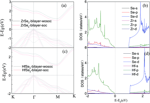 |
| | Fig. 2 Band structures of the ZrSe2 (a) and HfSe2 bilayers (c) with SOC (red solid lines) and without SOC (black solid lines), and only the corresponding partial density of states with SOC are represented in (b) and (d). The Fermi level is indicated as the dashed line at E = 0.0 eV. | |
Table 2 The calculated effective mass (m*) in the unit of free electron mass me, average mass (md), elastic modulus C2D, DP constant El, carrier mobility (μ), and relaxation time (τ) for the n- and p-type doped bilayers of ZrSe2 and HfSe2 at 300 K
| Material |
Carriers |
m* (M → Γ) |
m* (M → K) |
md |
C2D (eV Å−2) |
El (eV) |
μ (cm2 V−1 s−1) |
τ (10−13 s) |
| ZrSe2 |
e |
2.88 |
0.66 |
1.38 |
19.96 |
3.22 |
165.75 |
2.72 |
| h |
−0.21 |
−0.33 |
0.26 |
19.96 |
−8.82 |
1608.09 |
1.92 |
| HfSe2 |
e |
2.81 |
0.55 |
1.24 |
30.78 |
2.57 |
457.67 |
7.32 |
| h |
−0.20 |
−0.30 |
−0.24 |
30.78 |
−9.72 |
2322.60 |
2.64 |
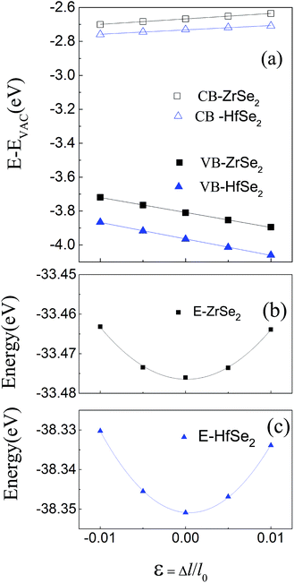 |
| | Fig. 3 (a) The energies of the band edge of VB and CB with respect to the lattice dilation ε = Δl/l0 in-plane, where l0 is the lattice constant. Vacuum levels are used as reference energy. Black and blue lines indicate the linear fit, the slopes of which correspond to the deformation potential constants for ZrSe2 and HfSe2 bilayers, respectively. (b) and (c) are the total energy versus relative change of lattice parameter in-plane. The black and blue lines are quadratic fitting curves for ZrSe2 and HfSe2 bilayers, respectively. From the fitting coefficient, the 2D effective elastic modulus C2D can be obtained. | |
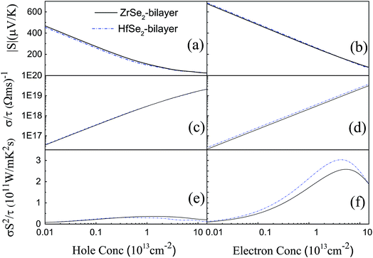 |
| | Fig. 4 The calculated transport coefficients (a and b) absolute values of Seebeck coefficient S, (c and d) the σ/τ, and (e and f) the σS2/τ for ZrSe2 (black solid line) and HfSe2 (blue dashed dot line) as a function of the carrier concentration n of hole (left) and electron (right). | |
3.3 Phonon transport properties
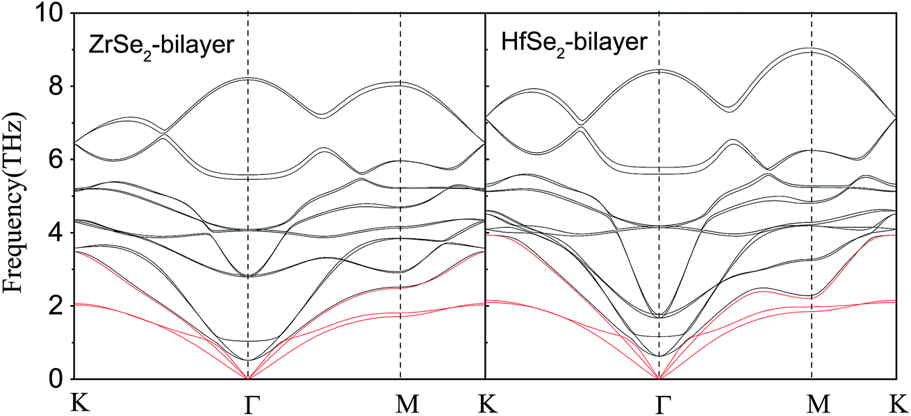
Now, we investigate the phonon transport properties of these bilayers. Fig. 5 shows the phonon dispersion relationship of the bilayer ZrSe2 (left panel) and HfSe2 (right panel), where the red solid lines represent the acoustic ZA, TA, and LA branches. As can be seen, there is no soft mode in the calculated phonon spectrum, confirming that these bilayers are dynamically stable. It can be seen from Fig. 5, firstly, the maximum frequencies of acoustic phonon modes of bilayer ZrSe2 and HfSe2 are 3.48 and 3.93 THz, respectively, which are quite a bit lower than those of 2H-MoSe2 (ref. 10) (4.5 THz) and 2H-MoS2 (ref. 9) (7.5 THz) monolayers. As is known such a low frequency displays a lower group velocity of the acoustic phonon modes in these systems, which is beneficial to obtaining a low lattice thermal conductivity. Secondly, in contrast to bulk MSe2,11 there is a strong coupling between the optical phonon modes and acoustic phonon modes in the bilayer MSe2, which enhances the chance of anharmonic phonon scattering, resulting in a reduced lattice thermal conductivity. Therefore, the two important characteristics are lower maximum frequency of acoustic phonon modes and strong coupling between optical and acoustic phonon modes, indicating that the two bilayers may exhibit low κl, which will be discussed below. As can be seen from Fig. 5, the frequency span of the HfSe2-bilayer is larger than that of the ZrSe2-bilayer, since the atomic mass difference between the Hf and Se elements is slightly larger than that between elements of Zr and Se. Compared to the ZrSe2 bilayer, there is a stronger coupling between acoustic and low-frequency optical branches in the HfSe2 bilayer, indicating a stronger anharmonic scattering and hence the lower lattice thermal conductivity of HfSe2 bilayer.
 |
| | Fig. 5 Phonon dispersions of bilayer ZrSe2 (left) and HfSe2 (right) from first-principles calculations, the acoustic ZA, TA and LA branches are highlighted in red. | |
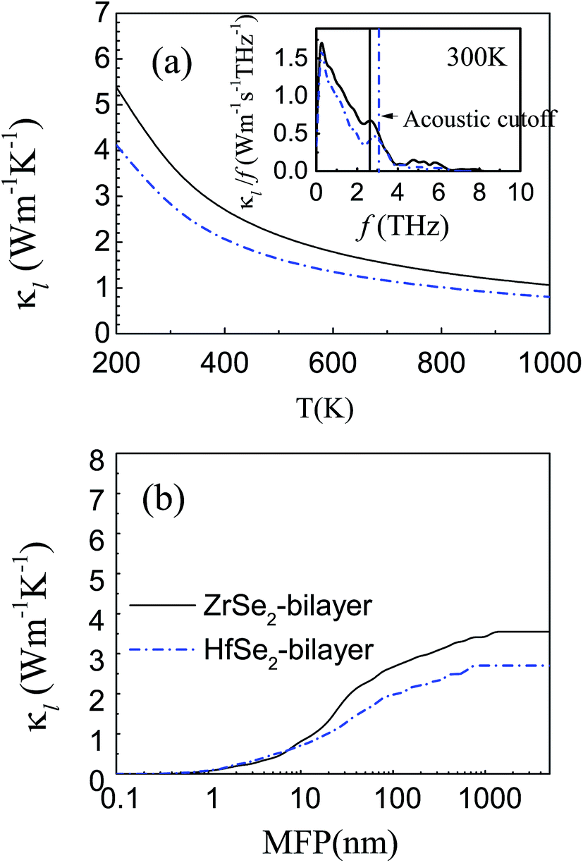
Calculated lattice thermal conductivity is shown in Fig. 6(a). As shown by the fitted curves, κl decreases approximately following a 1/T dependence with increasing temperature, indicating a dominant phonon scattering by the Umklapp process in these materials.70 Clearly, the lattice thermal conductivity κl for the HfSe2-bilayer is always lower than that of the ZrSe2-bilayer within the temperature range investigated, which is consistent with the above analysis. Specifically, the lattice thermal conductivity of the bilayers, ZrSe2 and HfSe2, are 3.55 and 2.7 W m−1 K−1 at room temperature, respectively. We find that the lattice thermal conductivity of the bilayer MSe2 is slightly higher than their monolayer configurations12,13 while much lower than those of their bulk counterparts from a previous study11 (about 9.9 and 7.7 W m−1 K−1 for ZrSe2 and HfSe2, respectively), which can be better explained from the viewpoint of the size effect. The inset in Fig. 6(a) displays the contribution of phonons with different frequencies to lattice thermal conductivity at 300 K. It can be seen that the acoustic branches probably contribute to more than about 80% of κl and the optical contribution to κl is extremely limited especially when frequencies are higher than 6 THz, indicating the acoustic contribution predominates. In order to further study the thermal conductivity, we show in Fig. 6(b) the cumulative thermal conductivity versus the phonon mean free path (MFP) at 300 K, which describes the contribution of different mean free path phonons towards the thermal conductivity. It can be seen that the κl for HfSe2-bilayer is primarily contributed by the phonons with MFPs up to 700 nm, while for ZrSe2-bilayer the allowed MFP expands to 1 μm. Meanwhile, the smaller MFP of the HfSe2-bilayer also indicates a higher scattering probability of phonons and hence the suppressed κl as discussed above.
 |
| | Fig. 6 (a) Calculated temperature dependence of phonon thermal conductivity from 200 K to 1000 K obtained from pBTE with the inset map of κl contribution with respect to frequency at 300 K. (b) The cumulative phonon thermal conductivity versus phonon mean free path at room temperature. The black solid line and the blue dashed dot line represent ZrSe2 and HfSe2 bilayers, respectively. | |
3.4 Thermoelectric figure of merit ZT
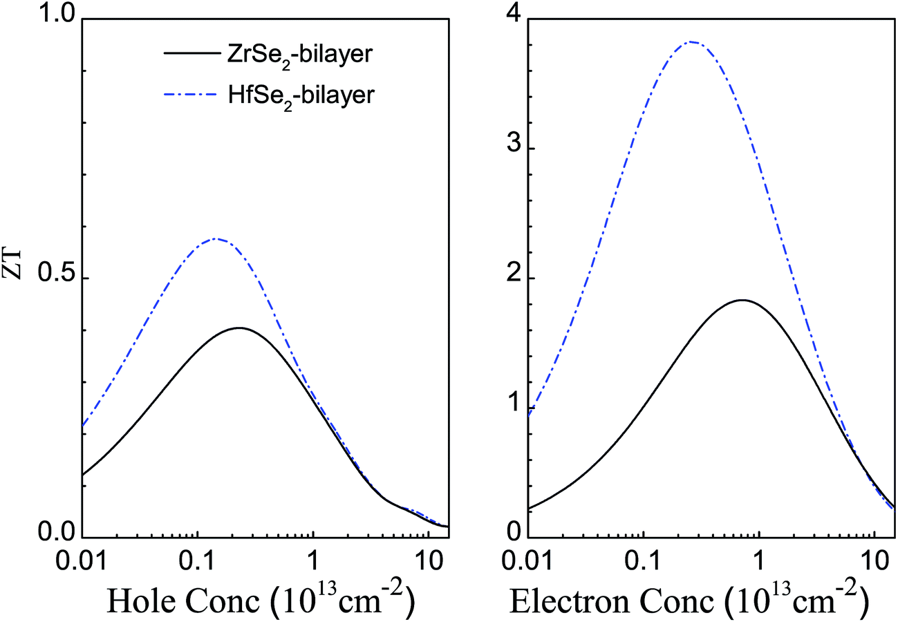
Next, we calculate the dimensionless figure of merit ZT combined effect of electronic and thermal properties on the thermoelectric efficiency of these materials. Firstly, the total thermal conductivity is estimated by considering both the electronic and lattice contributions using the equation: κtotal = κe + κl, detailed computation methods are demonstrated in the above computational details. And κtotal at room temperature for the n- and p-types of these bilayers are summarized in Table 3. Fig. 7 shows the evaluated ZT of these bilayers for p-type (left panel) and n-type (right panel) doping at room temperature. Clearly, there is an optimum carrier concentration required to obtain the maximum ZT values because of the trade-off relationship between S and σ as shown in Fig. 4. At room temperature, the optimum carrier concentrations, the corresponding Seebeck coefficient S, electrical conductivity σ, as well as ZTs are shown in Table 3. In comparison with the p-doped case, the n-doped bilayers exhibit higher ZT values due to the better transport performance of the electrons. In addition, the values of ZT for bilayer HfSe2 are larger than that of the bilayer ZrSe2 for both n- and p-type doping, resulting from the better electronic transport properties and lower lattice thermal conductivity as discussed above. The optimal n-type ZT values for ZrSe2 and HfSe2 bilayers are 1.84 at the carrier concentration of 7.85 × 1012 cm−2 and 3.83 at the carrier concentration of 2.37 × 1012 cm−2, respectively, which are much higher than not only their bulk counterparts and monolayer but also some other existing 2D thermoelectric materials reported previously. For instance, the optimal ZT (theoretical value) for monolayer PdSe2 (ref. 71) at 300 K and SnSe2 (ref. 72) at 600 K are about 1.1 and 0.94 (theoretical value), respectively, and only about 0.1 (theoretical value) for MoS2 (ref. 9) at 500 K. Although the optimal p-type ZT values, about 0.41 and 0.58 for ZrSe2 and HfSe2 bilayers at 300 K, respectively, are much lower than that of n-type, they are still much higher than that of their bulk counterparts, which do not exceed 0.1 as predicted previously.11
Table 3 Summary of the important parameters and results for the n- and p-type doped ZrSe2 and HfSe2 bilayers. The optimal carrier concentration nopt yielding the maximum attainable value of ZT, the Seebeck coefficient, electrical conductivity and total thermal conductivity at optimal doping at 300 K
| Material |
Carriers |
nopt (1012 cm−2) |
S (μV K−1) |
σ (105 Ω−1 m−1) |
κ (W m−1 K−1) |
ZT |
| ZrSe2 |
e |
7.85 |
−303 |
4.57 |
6.89 |
1.84 |
| h |
2.13 |
212 |
1.35 |
4.54 |
0.41 |
| HfSe2 |
e |
2.37 |
−413 |
4.45 |
5.96 |
3.83 |
| h |
1.36 |
234 |
1.27 |
3.62 |
0.58 |
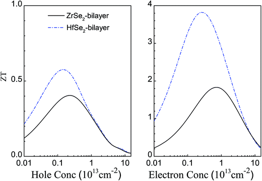 |
| | Fig. 7 Estimated figure of merits of bilayer ZrSe2 (black solid line) and HfSe2 (blue dashed dot line) for both p- (left panel) and n-type (right panel) at 300 K. | |
4 Summary and conclusions
In summary, using first-principles calculations in combination with Boltzmann transport theory, we have investigated the electronic and thermoelectric transport properties for ZrSe2 and HfSe2 bilayers. The van der Waals (vdW) interactions, on-site Hubbard U parameter and spin–orbit coupling have been included in calculations to correctly describe the electronic properties of the considered systems. The degenerate conduction bands and stair-like 2D DOS contribute to the high n-type Seebeck coefficient and power factor. In addition, they exhibit rather low lattice thermal conductivity comparable to their individual bulk. Overall, the dimensionless figure of merit at room temperature are predicted as high as 1.84 (3.83) and 0.41 (0.58) for n- and p-doped ZrSe2 (HfSe2) bilayers, respectively, which are superior to those of some monolayer TMDCs and other popular thermoelectric materials. The present work indicates that bilayers of ZrSe2 and HfSe2 are promising thermoelectric materials preferable to their bulk counterparts. Although a lot of monolayer systems have been studied as promising 2D thermoelectric materials, studies on the corresponding bilayer or multilayer configurations are rare. Our findings show that tuning the atomic layers of 2D TMDCs is an effective approach to further optimize their thermoelectric performance.
Conflicts of interest
There are no conflicts to declare.
Acknowledgements
Authors gratefully acknowledge the financial support from the National Natural Science Foundation of China (Grant No. 11804040 and Grant No. 51401031) and Shandong Science and Technology Project (Grant No. J15LK52).
References
- Y. Pei, X. Shi, A. Lalonde, H. Wang, L. Chen and G. Snyder, Nature, 2011, 473, 66–69 CrossRef CAS PubMed.
- Y. Ma, R. Heijl and A. E. C. Palmqvist, J. Mater. Sci., 2013, 48, 2767–2778 CrossRef CAS.
- T. Zhu, Y. Liu, C. Fu, J. P. Heremans, J. G. Snyder and X. Zhao, Adv. Mater., 2017, 29, 1605884 CrossRef PubMed.
- T. Fang, S. Zheng, T. Zhou, L. Yan and P. Zhang, Phys. Chem. Chem. Phys., 2017, 19, 4411–4417 RSC.
- J. P. A. Makongo, D. K. Misra, X. Zhou, A. Pant, M. R. Shabetai, X. Su, C. Uher, K. L. Stokes and P. F. P. Poudeu, J. Am. Chem. Soc., 2011, 133, 18843–18852 CrossRef CAS PubMed.
- Y. Liu, P. Sahoo, J. P. A. Makongo, X. Zhou, S.-J. Kim, H. Chi, C. Uher, X. Pan and P. F. P. Poudeu, J. Am. Chem. Soc., 2013, 135, 7486–7495 CrossRef CAS PubMed.
- T. Zhu, C. Fu, H. Xie, Y. Liu and X. Zhao, Adv. Energy Mater., 2015, 5, 1500588 CrossRef.
- W. Zhang, Z. Huang, W. Zhang and Y. Li, Nano Res., 2014, 7, 1731–1737 CrossRef CAS.
- Z. Jin, Q. Liao, H. Fang, Z. Liu, W. Liu, Z. Ding, T. Luo and N. Yang, Sci. Rep., 2015, 5, 18342 CrossRef CAS PubMed.
- S. Kumar and U. Schwingenschlögl, Chem. Mater., 2015, 27, 1278–1284 CrossRef CAS.
- G. Yumnam, T. Pandey and A. K. Singh, J. Chem. Phys., 2015, 143, 234704 CrossRef PubMed.
- G. Ding, G. Gao, Z. Huang, W. Zhang and K. Yao, Nanotechnology, 2016, 27, 375703 CrossRef PubMed.
- D. Qin, X.-J. Ge, G.-q. Ding, G.-y. Gao and J.-T. Lü, RSC Adv., 2017, 7, 47243–47250 RSC.
- G. Li, K. Yao and G. Gao, Nanotechnology, 2017, 29, 015204 CrossRef PubMed.
- H. Y. Lv, W. J. Lu, D. F. Shao, H. Y. Lu and Y. P. Sun, J. Mater. Chem. C, 2016, 4, 4538–4545 RSC.
- A. Kumar and P. K. Ahluwalia, Eur. Phys. J. B, 2012, 85, 186 CrossRef.
- R.-N. Wang, G.-Y. Dong, S.-F. Wang, G.-S. Fu and J.-L. Wang, Phys. Chem. Chem. Phys., 2017, 19, 5797–5805 RSC.
- A. Kumar, H. He, R. Pandey, P. Ahluwalia and K. Tankeshwar, Phys. Chem. Chem. Phys., 2015, 17, 19215–19221 RSC.
- P. E. Blöchl, Phys. Rev. B: Condens. Matter Mater. Phys., 1994, 50, 17953–17979 CrossRef.
- G. Kresse and J. Furthmüller, Phys. Rev. B: Condens. Matter Mater. Phys., 1996, 54, 11169 CrossRef CAS.
- G. Kresse and J. Hafner, Phys. Rev. B: Condens. Matter Mater. Phys., 1993, 47, 558 CrossRef CAS.
- G. Kresse, Phys. Rev. B: Condens. Matter Mater. Phys., 1999, 59, 1758 CrossRef CAS.
- J. P. Perdew, K. Burke and M. Ernzerhof, Phys. Rev. Lett., 1996, 77, 3865–3868 CrossRef CAS PubMed.
- S. Grimme, J. Antony, S. Ehrlich and H. Krieg, J. Chem. Phys., 2010, 132, 154104 CrossRef PubMed.
- Z. Fang, I. V. Solovyev, H. Sawada and K. Terakura, Phys. Rev. B: Condens. Matter Mater. Phys., 1999, 59, 762 CrossRef CAS.
- H. J. Kulik and N. Marzari, J. Chem. Phys., 2011, 134, 094103 CrossRef PubMed.
- A. Kumar, H. He, R. Pandey, P. Ahluwalia and K. Tankeshwar, AIP Conf. Proc., 2015, 090016 CrossRef.
- S.-D. Guo and J.-L. Wang, Semicond. Sci. Technol., 2016, 31, 095011 CrossRef.
- X.-J. Ge, D. Qin, K.-L. Yao and J.-T. Lü, J. Phys. D: Appl. Phys., 2017, 50, 405301 CrossRef.
- S.-D. Guo, J. Alloys Compd., 2016, 663, 128–133 CrossRef CAS.
- D. Greenaway and R. Nitsche, J. Phys. Chem. Solids, 1965, 26, 1445–1458 CrossRef CAS.
- H. L. Zhuang and R. G. Hennig, J. Phys. Chem. C, 2013, 117, 20440–20445 CrossRef CAS.
- T. Scheidemantel, C. Ambrosch-Draxl, T. Thonhauser, J. Badding and J. Sofo, Phys. Rev. B: Condens. Matter Mater. Phys., 2003, 68, 125210 CrossRef.
- L. Jodin, J. Tobola, P. Pecheur, H. Scherrer and S. Kaprzyk, Phys. Rev. B: Condens. Matter Mater. Phys., 2004, 70, 184207 CrossRef.
- L. Chaput, P. Pécheur, J. Tobola and H. Scherrer, Phys. Rev. B: Condens. Matter Mater. Phys., 2005, 72, 085126 CrossRef.
- G. K. Madsen and D. J. Singh, Comput. Phys. Commun., 2006, 175, 67–71 CrossRef CAS.
- X. Yang, Z. Dai, Y. Zhao, J. Liu and S. Meng, J. Phys.: Condens. Matter, 2018, 30, 425401 CrossRef PubMed.
- J. Bardeen and W. Shockley, Phys. Rev., 1950, 80, 72 CrossRef CAS.
- F. Beleznay, F. Bogár and J. Ladik, J. Chem. Phys., 2003, 119, 5690–5695 CrossRef CAS.
- L.-C. Zhang, G. Qin, W.-Z. Fang, H.-J. Cui, Q.-R. Zheng, Q.-B. Yan and G. Su, Sci. Rep., 2016, 6, 19830 CrossRef CAS PubMed.
- Y. Cai, G. Zhang and Y.-W. Zhang, J. Am. Chem. Soc., 2014, 136, 6269–6275 CrossRef CAS PubMed.
- M.-Q. Long, L. Tang, D. Wang, L. Wang and Z. Shuai, J. Am. Chem. Soc., 2009, 131, 17728–17729 CrossRef CAS PubMed.
- M. Long, L. Tang, D. Wang, Y. Li and Z. Shuai, ACS Nano, 2011, 5, 2593–2600 CrossRef CAS PubMed.
- Y. Pei, A. D. LaLonde, H. Wang and G. J. Snyder, Energy Environ. Sci., 2012, 5, 7963–7969 RSC.
- J. Xi, M. Long, L. Tang, D. Wang and Z. Shuai, Nanoscale, 2012, 4, 4348–4369 RSC.
- K. Parlinski, Z. Q. Li and Y. Kawazoe, Phys. Rev. Lett., 1997, 78, 4063–4066 CrossRef CAS.
- M. Chen and R. Podloucky, Phys. Rev. B: Condens. Matter Mater. Phys., 2013, 88, 045134 CrossRef.
- J. M. Ziman, Principles of the Theory of Solids, Cambridge University Press, 1979 Search PubMed.
- W. Li, J. Carrete, N. A. Katcho and N. Mingo, Comput. Phys. Commun., 2014, 185, 1747–1758 CrossRef CAS.
- A. Togo, F. Oba and I. Tanaka, Phys. Rev. B: Condens. Matter Mater. Phys., 2008, 78, 134106 CrossRef.
- W. Li, N. Mingo, L. Lindsay, D. A. Broido, D. A. Stewart and N. A. Katcho, Phys. Rev. B: Condens. Matter Mater. Phys., 2012, 85, 195436 CrossRef.
- W. Li, L. Lindsay, D. Broido, D. A. Stewart and N. Mingo, Phys. Rev. B: Condens. Matter Mater. Phys., 2012, 86, 174307 CrossRef.
- H. Kim, J. Korean Phys. Soc., 2014, 64, 547–553 CrossRef CAS.
- M. Abdulsalam and D. Joubert, Comput. Mater. Sci., 2016, 115, 177–183 CrossRef CAS.
- Q. Zhao, Y. Guo, K. Si, Z. Ren, J. Bai and X. Xu, Phys. Status Solidi B, 2017, 254, 1700033 CrossRef.
- R. Mas-Balleste, C. Gomez-Navarro, J. Gomez-Herrero and F. Zamora, Nanoscale, 2011, 3, 20–30 RSC.
- K. S. Novoselov, D. Jiang, F. Schedin, T. J. Booth, V. V. Khotkevich, S. V. Morozov and A. K. Geim, Proc. Natl. Acad. Sci. U. S. A., 2005, 102, 10451–10453 CrossRef CAS PubMed.
- S. Mañas-Valero, V. García-López, A. Cantarero and M. Galbiati, Appl. Sci., 2016, 6, 264 CrossRef.
- A. Castellanos-Gomez, M. Barkelid, A. M. Goossens, V. E. Calado, H. S. J. van der Zant and G. A. Steele, Nano Lett., 2012, 12, 3187–3192 CrossRef CAS PubMed.
- A. M. van der Zande, P. Y. Huang, D. A. Chenet, T. C. Berkelbach, Y. You, G.-H. Lee, T. F. Heinz, D. R. Reichman, D. A. Muller and J. C. Hone, Nat. Mater., 2013, 12, 554–561 CrossRef CAS PubMed.
- S. Najmaei, Z. Liu, W. Zhou, X. Zou, G. Shi, S. Lei, B. I. Yakobson, J.-C. Idrobo, P. M. Ajayan and J. Lou, Nat. Mater., 2013, 12, 754–759 CrossRef CAS PubMed.
- J. N. Coleman, M. Lotya, A. ONeill, S. D. Bergin, P. J. King, U. Khan, K. Young, A. Gaucher, S. De and R. J. Smith, et al., Science, 2011, 331, 568–571 CrossRef CAS PubMed.
- A. P. V. Rakkini and K. Mohanraj, Ionics, 2018, 24, 1243–1252 CrossRef CAS.
- D. T. Hodul and A. M. Stacy, J. Solid State Chem., 1984, 54, 438–446 CrossRef CAS.
- R. Yue, A. T. Barton, H. Zhu, A. Azcatl, L. F. Pena, J. Wang, X. Peng, N. Lu, L. Cheng and R. Addou, et al., ACS Nano, 2015, 9, 474–480 CrossRef CAS PubMed.
- A. Hong, L. Li, R. He, J. Gong, Z. Yan, K. Wang, J.-M. Liu and Z. Ren, Sci. Rep., 2016, 6, 22778 CrossRef CAS PubMed.
- H. Peng, N. Kioussis and G. J. Snyder, Phys. Rev. B: Condens. Matter Mater. Phys., 2014, 89, 195206 CrossRef.
- K. S. Novoselov, D. Jiang, F. Schedin, T. J. Booth, V. V. Khotkevich, S. V. Morozov and A. K. Geim, Proc. Natl. Acad. Sci., 2005, 102, 10451–10453 CrossRef CAS PubMed.
- J. Sun and D. J. Singh, Phys. Rev. Appl., 2016, 5, 024006 CrossRef.
- A. Ward, D. A. Broido, D. A. Stewart and G. Deinzer, Phys. Rev. B: Condens. Matter Mater. Phys., 2009, 80, 125203 CrossRef.
- D. Qin, Y. Peng, G. Ding, X. Ge, H. Song and G. Gao, Sci. Rep., 2018, 8, 1–8 CrossRef CAS PubMed.
- G. Li, G. Ding and G. Gao, J. Phys.: Condens. Matter, 2017, 29, 015001 CrossRef PubMed.
|
| This journal is © The Royal Society of Chemistry 2019 |
Click here to see how this site uses Cookies. View our privacy policy here. 
 Open Access Article
 This Open Access Article is licensed under a Creative Commons Attribution-Non Commercial 3.0 Unported Licence
 b,
Guang-qian Ding
b,
Guang-qian Ding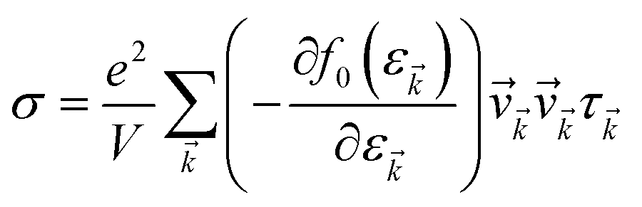
 , where
  and
and  are the effective mass parallel and perpendicular to the transport direction. For the two-dimensional (2D) system, the effective elastic modulus C2D in-plane is calculated through C2D = (∂2E/∂ε2)/S0, where E, ε and S0 are, respectively, the total energy, the applied small strain (by a step of 0.5% in the present study), and the area of the investigated system. El is the deformation potential constant which can be obtained by El = dEedge/dε, where Eedge is the energy of the band edges (VBM and CBM). Finally, the estimation results on carrier mobility, μ and the effective mass, m* can be used to calculate the scattering time, τ using the following formula