
 Open Access Article
 This Open Access Article is licensed under a Creative Commons Attribution-Non Commercial 3.0 Unported Licence
The design and fabrication of a multilayered graded GNP/Ni/PMMA nanocomposite for enhanced EMI shielding behavior†
Hye Ji Ima,
Jae Young Ohc,
Seongwoo Ryub and
Soon Hyung Hong *a
*a
aDepartment of Materials Science and Engineering, Korea Advanced Institute of Science and Technology (KAIST), 291 Daehak-ro, Yuseong-gu, Daejeon, 34141, Republic of Korea. E-mail: shhong@kaist.ac.kr; Tel: +82 42 350 3327
bDepartment of Advanced Materials Engineering, The University of Suwon, 17, Wauan-gil, Bongdam-eup, Hwaseong-si, Gyeonggi-do, Republic of Korea
cSK Hynix Inc, 2091, Gyeongchung-daero, Bubal-eub, Icheon-si, Gyeonggi-do, Republic of Korea
First published on 10th April 2019
Abstract
A multilayered graded structure can maximize the electromagnetic interference (EMI) shielding properties of a nanocomposite for a specific amount of a conductive filler in a polymer matrix. In this study, multilayered graded nanocomposites of graphene nanoplatelet (GNP)/Ni/polymethyl methacrylate (PMMA) were developed to achieve enhanced EMI shielding behavior. Both multilayered and monolayered nanocomposites were fabricated by controlling the compositions of GNP/Ni in the PMMA matrix. The contributions of the multilayered nanocomposite to EMI shielding were investigated and compared with the shielding effectiveness of the monolayered nanocomposite. The multilayered nanocomposite shows enhanced shielding effectiveness of around 61 dB in the X-band, which is more than three orders of magnitude higher than that of the monolayered nanocomposite. It has been confirmed that the measurements of reflection, absorption and total shielding effectiveness are in good accordance with the theoretically calculated results. The primary shielding mechanism was absorption due to conductive dissipation. The enhanced absorption of electromagnetic waves is attributed to an abrupt increase in the conductivity between layers in the direction of wave propagation in a multilayered nanocomposite due to impedance matching with the air and internal reflection between layers.
1. Introduction
Electromagnetic interference (EMI), especially in the high-frequency range of 8–12 GHz (the X-band), has led to problems in various fields where electromagnetic devices and military systems are used.1–3 The degradation in the performances of control and communication systems and the leakage of information from military systems has increased the demand for EMI shielding materials.4–6Metals, which have been used as conventional EMI shielding materials, have recently been found to suffer from reflection from their surfaces, corrosion susceptibility and high density.6–9 As a promising candidate for an EMI shielding material, graphene has gained attention due to its high electrical conductivity, low density and anti-corrosion resistance.10–12 Since graphene produced via mechanical exfoliation or chemical vapor deposition has limitations in productivity,13,14 the use of graphene nanoplatelet (GNP) is more suitable for industrial applications.15 GNP, composed of hundreds of graphite layers stacked together and with an average thickness between 30 and 100 nm, can offer more advantages such as higher intrinsic conductivity, much lower production cost and larger-scale production.16,17
In our previous study, nano-sized Ni particle-decorated GNP has been fabricated via a molecular-level mixing process, and its shielding capability has been investigated.15 The EMI shielding effectiveness (SE) of the GNP/Ni powders mixed in wax (30 wt%) is around 40 dB, whereas GNP itself (30 wt%) shows the SE of around 26 dB in the X-band. As a result of electrostatic interaction between Ni2+ ions and the functional groups on GNP, Ni nanoparticles are homogeneously anchored on GNP, and chemical bonds are formed between them.18 Chemical bonds play important roles in the enhancement of the absorption capability, providing magnetic dipoles that interact with magnetic wave and facilitating charge transfer between GNP and Ni nanoparticles. In addition, homogeneous distribution of nanoparticles promotes efficient formation of conductive networks while preventing agglomeration of GNP in a matrix; this leads to an increase in the electrical conductivity and EMI SE.
The application of the GNP/Ni nanocomposite as an EMI shielding material can be realized by adding GNP/Ni as a filler in a polymer matrix. The polymer matrix is lightweight and provides corrosion resistance and excellent processability to GNP/Ni.1,8 The GNP/Ni nanocomposite in the polymer matrix is expected to exhibit improved shielding capability by forming conductive networks of the GNP/Ni filler due to its high aspect ratio and electrical conductivity.19,20 This is because the EMI shielding properties of the polymer nanocomposite incorporating the conductive filler are dependent on the aspect ratio, intrinsic conductivity and the amount of filler.21,22
Increasing the amount of the GNP/Ni filler is an indispensable choice to improve the EMI shielding performance.10 However, this leads to agglomeration, which deteriorates the electrical conductivity and reflection of incident wave from the surface; this induces interference of the reflected wave. Thus, it is highly desirable that the incident wave must enter and be attenuated through a material to prevent additional interference.23 Therefore, materials designed with multilayered structures with an increasing amount of conductive fillers can solve the previous challenges while preserving an average amount of fillers.24
Herein, we report a multilayered structure of GNP/Ni/polymethyl methacrylate (PMMA) nanocomposite with enhanced EMI shielding capability; moreover, this study involves the maximization of the EMI shielding properties of the GNP/Ni nanocomposite present in a specific amount in a matrix. To investigate the contribution of the multilayered structure to EMI shielding, multilayered nanocomposites with abrupt variation in the GNP/Ni concentration between layers and monolayered nanocomposites were designed and fabricated. The SE values of the two structures with the same total amount of GNP/Ni and sample thickness were compared with each other. Furthermore, the mechanism of EMI shielding of the multilayered nanocomposite was analyzed based on theoretical calculations.
2. Materials and methods
2.1 Materials
Graphene nanoplatelets (GNP) and polymethyl methacrylate (PMMA) were acquired from LG Chem. Ethylene glycol (99%) and hydrazine monohydrate (98%) were purchased from Junsei Chemical. Nickel(II) acetate (Ni(CH3CO2)2·(H2O)4) and polyvinyl pyrrolidone (PVP, Mw = 55![[thin space (1/6-em)]](https://www.rsc.org/images/entities/char_2009.gif) 000 g mol–1) were purchased from Sigma-Aldrich.
000 g mol–1) were purchased from Sigma-Aldrich.
2.2 Fabrication of GNP/Ni by the molecular-level mixing process
GNP (500 mg) was dispersed in ethylene glycol (500 mL) by sonication for 2 h. Ni(CH3CO2)2·(H2O)4 (0.966 g) was added and mixed with the GNP solution (at the volume ratio of GNP/Ni about 9:1). Then, aqueous 2 M NaOH (5 mL) was added to the GNP/Ni ion solution, and the mixed solution was heated to 60 °C. This process involves a chemical reaction that results in the oxidation of Ni ions to NiO and the formation of oxidized nano-sized powders. Subsequently, hydrazine monohydrate (5 mL) was introduced with continuous heating at 60 °C. The oxidized nanocomposite was reduced via the introduction of hydrazine monohydrate. After cooling the mixture, it was then filtered and rinsed with ethanol. The powders were dried at 80 °C under vacuum and reduced into the GNP/Ni nanocomposite powders at 400 °C in 3 h under a hydrogen atmosphere.
2.3 Fabrication of the GNP/Ni/PMMA nanocomposite
Each layer of the GNP/Ni/PMMA nanocomposite (20 wt%, 30 wt% and 40 wt% of GNP/Ni in PMMA, separately) was prepared by solution blending. For each layer, the GNP/Ni powders were separately dispersed with PVP and PMMA in chloroform under stirring. The two mixtures were blended for 1–3 h at 65 °C under stirring until the solvent was evaporated, and then, they were dried under vacuum at 60 °C to completely remove the solvent. This process leads to homogeneous dispersion of GNP/Ni inside the PMMA layer. For abrupt concentration changes between layers, each layer was packed in a mold and pressed isostatically at room temperature under a pressure of 27 MPa for 10 min. Then, the GNP/Ni/PMMA samples were cut in a rectangular shape with the thickness of 2.5 mm (Fig. S1†).2.4 Characterization
The microstructures of the samples were investigated by a scanning electron microscope (SEM, Hitachi S-4800). The electrical conductivities were measured using a four-point probe (AIT CMT-SR1000N). For the EMI SE measurement of the GNP/Ni/PMMA nanocomposite, a two-port vector network analyzer (Agilent 8722ES) was used to measure scattering parameters (S12 and S11) by the waveguide method between 8 and 12 GHz. The samples were placed between two sections of the waveguide.Transmission coefficient (T), reflection coefficient (R) and absorption coefficient (A) can be calculated from S12 and S11 by the following equations:
| T = |S12|2 = |Et/Ei|2 | (1) |
| R = |S11|2 = |Er/Ei|2 | (2) |
| A + R + T = 1 | (3) |
3. Results and discussion
3.1 Monolayered and multilayered GNP/Ni/PMMA nanocomposites for EMI shielding
Fig. 1 shows the schematic of the monolayered and multilayered GNP/Ni/PMMA nanocomposites. The monolayered and multilayered nanocomposites were designed based on the same average amount of GNP/Ni (30 wt%) and sample thickness (2.5 mm). The monolayered GNP/Ni/PMMA nanocomposite {30 wt% GNP/Ni in PMMA} shown in Fig. 1(a) was fabricated by a general solution blending process, and its cross-section SEM images are shown in Fig. S2.† The GNP/Ni powders were observed to be homogeneously dispersed in the PMMA matrix. Fig. 1(b) depicts the image of the multilayered GNP/Ni/PMMA nanocomposite ({20 wt% GNP/Ni in PMMA}/{30 wt% GNP/Ni in PMMA}/{40 wt% GNP/Ni in PMMA}). The average amount of GNP/Ni in PMMA was kept constant at 30 wt%, and the amount of GNP/Ni for each layer inside the shielding material was changed; the concentration difference of GNP/Ni between layers was maintained at 10 wt%, and the top (the 1st), middle (2nd) and bottom (3rd) layer contained 20 wt%, 30 wt% and 40 wt% of GNP/Ni, respectively, in the direction of the propagation of incident wave. The 1st layer {20 wt% GNP/Ni} adopts less amount of conductive filler than the monolayered sample; this can lead to higher impedance (Z1). The reflection of incident waves results from the mismatch of impedance between the material's surface and the air.23 As the GNP/Ni concentration in the surface of the material decreases, the impedance gap between the material and the air becomes smaller. Therefore, this structure can maximize the fraction of incident wave that enters the material by minimizing the impedance gap between the 1st layer and the air.24 The 1st layer presents an intense penetrating capability, and the following layers have stronger absorption and reflection capability. As the concentration of GNP/Ni in a layer increases from top to bottom, the conductivity of the layer increases, and the impedance decreases; this results in an increase in both the reflection and the absorption capability. The wave approaching the multilayered structure can enter deeper through the material and can be more fully attenuated by the GNP/Ni filler than that when a monolayered nanocomposite is used.23,24 In addition, an abrupt concentration difference of 10 wt% between contacting layers induces an additional internal reflection between layers. Since the thickness of each layer is larger than the skin depth, which is the distance up to which the intensity of a wave decreases to 1/e of its original strength,9 waves reflected between layers dissipate into heat energy.25 This factor can be added to the SEA of the mutilayered structure. For these reasons, the multilayered structure can improve the shielding capability of a material without increasing the total amount of GNP/Ni.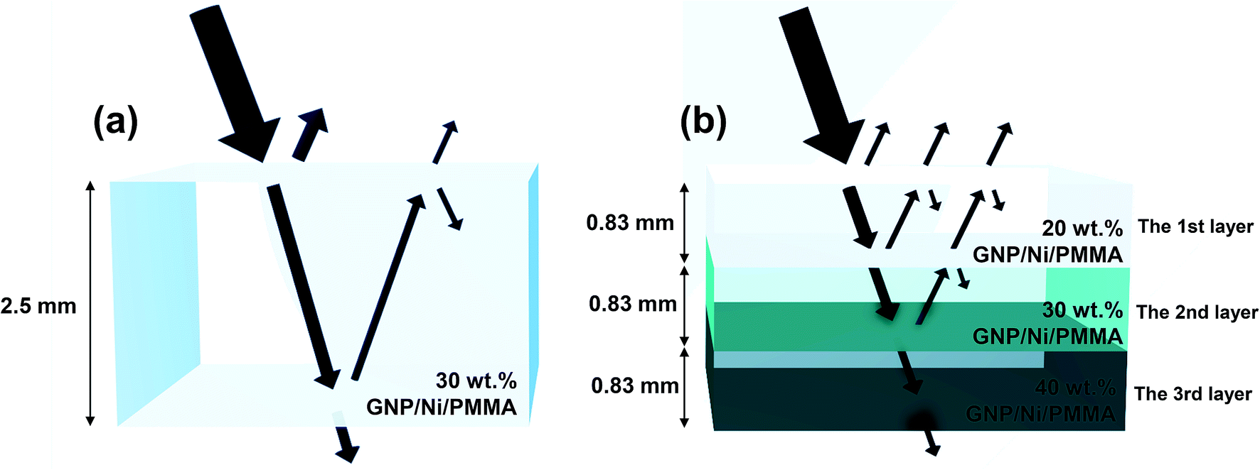 | ||
| Fig. 1 Schematic of the (a) monolayered GNP/Ni/PMMA nanocomposite {30 wt% GNP/Ni} and (b) multilayered GNP/Ni/PMMA nanocomposite ({20 wt% GNP/Ni}/{30 wt% GNP/Ni}/{40 wt% GNP/Ni}) (impedance of the nth layer (Zn): Z1 > Z2 > Z3). Monolayered and multilayered nanocomposites have the same average amount of GNP/Ni (30 wt%) and total specimen thickness (2.5 mm). | ||
The EMI SE of a material can be defined as the ratio of the incident power (energy) to the transmitted power (energy),
|
SE (dB) = 10log(Pi/Pt) = 20log(Ei/Et)
| (4) |
| SET = SER + SEA + SEM | (5) |
Since the skin depth is larger than the thickness of each layer, the internal reflection between layers due to difference in impedances is considered as absorption, which has been discussed in detail in Section 3.2. Therefore, the effective absorbance (Aeff) with respect to the power of the effective incident wave inside the material can be expressed as eqn (6).
| Aeff = (1 − R − T)/(1 − R) | (6) |
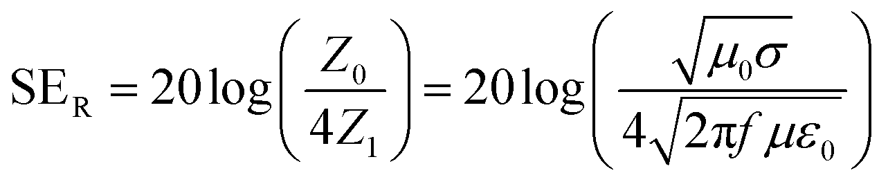
SER and SEA are calculated from transmission, reflection and absorption coefficients using the eqn (7) and (8), respectively.27
|
SER = −10log(1 − R)
| (7) |
|
SEA = −10log(1 − Aeff) = −10log[T/(1 − R)]
| (8) |
Fig. 2 shows the SER, SEA and SET values in the X-band of the monolayered and multilayered GNP/Ni/PMMA nanocomposites represented in Fig. 1. In Fig. 2(a) and (b), the mutilayered structure has lower SER and higher SEA values than the monolayered structure over the whole frequency range; this means much less incident wave from air reflects off the 1st layer in the mutilayered structure than that in the case of the monolayered structure; as a result, a bigger fraction of the incident energy penetrates the surface of the material and attenuated through the material. As the impedance reaches closer to that of air, the reflection of the incoming waves from the surface decreases; thus, SER and additional interference of the reflected wave are reduced.24,28 Fig. S3† depicts the impedances calculated for each layer in the multilayered nanocomposite at 8, 9, 10, 11 and 12 GHz. The 1st layer has the impedances of 86 Ω and 48 Ω at 8 GHz and 12 GHz, which are higher than those in the 2nd layer with the same impedance as in the monolayered structure (23 Ω and 17 Ω), respectively. The impedance of the 1st layer in the mutilayered structure is closer to that of air, i.e. 377 Ω, than to that of the monolayered structure. The impedance gap between the 1st layer and the air decreases with the decreasing amount of GNP/Ni. The reflection of waves incident to the material surface occurs due to impedance difference between them. A decrease in the impedance gap leads to a decrease in the overall reflection from the surface when a wave is incident and an increase in penetration through the material.29
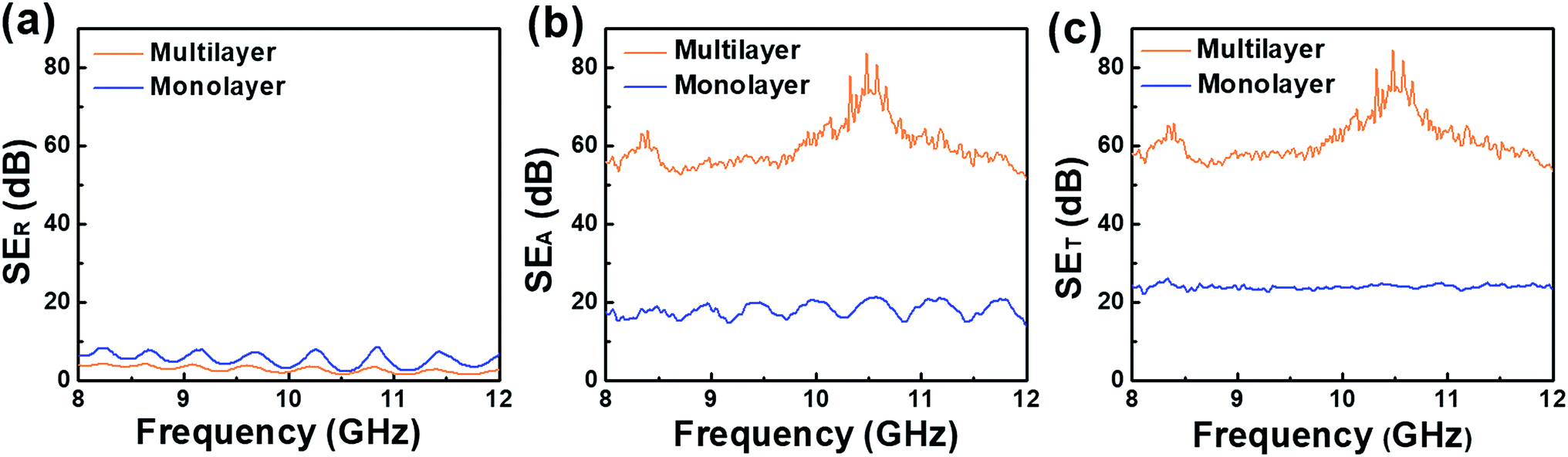 | ||
| Fig. 2 (a) SER, (b) SEA and (c) SET results of the monolayered and multilayered GNP/Ni/PMMA nanocomposites in Fig. 1(a) and (b). | ||
In Fig. 2(c), the SET value of the multilayered GNP/Ni/PMMA is 54–85 dB, whereas that of the monolayered sample is 22–26 dB for the same thickness. The major shielding mechanism in the multilayered structure is absorption by conductive dissipation. According to the SE results for the GNP/Ni/PMMA nanocomposite, the mutilayered structure shows superior shielding capability over the monolayered structure.
3.2 Theoretical and experimental results of the multilayered GNP/Ni/PMMA nanocomposite
To understand the mechanism of EMI shielding in the multilayered GNP/Ni/PMMA nanocomposite, as shown in Fig. 1(b), a theoretical calculation was carried out through plane-wave shielding theory developed for multiple sheets,30 and the results were compared with the experimental results.For the calculation of the magnetic permeability of each layer in the GNP/Ni/PMMA nanocomposite, each single layer of {20 wt% GNP/Ni}, {30 wt% GNP/Ni} and {40 wt% GNP/Ni} is respectively fabricated, and its SEA is measured (Fig. 3(a)). The relative magnetic permeability can be calculated using eqn (9), as shown in Fig. 3(b),
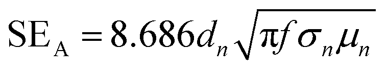 | (9) |
 | (10) |
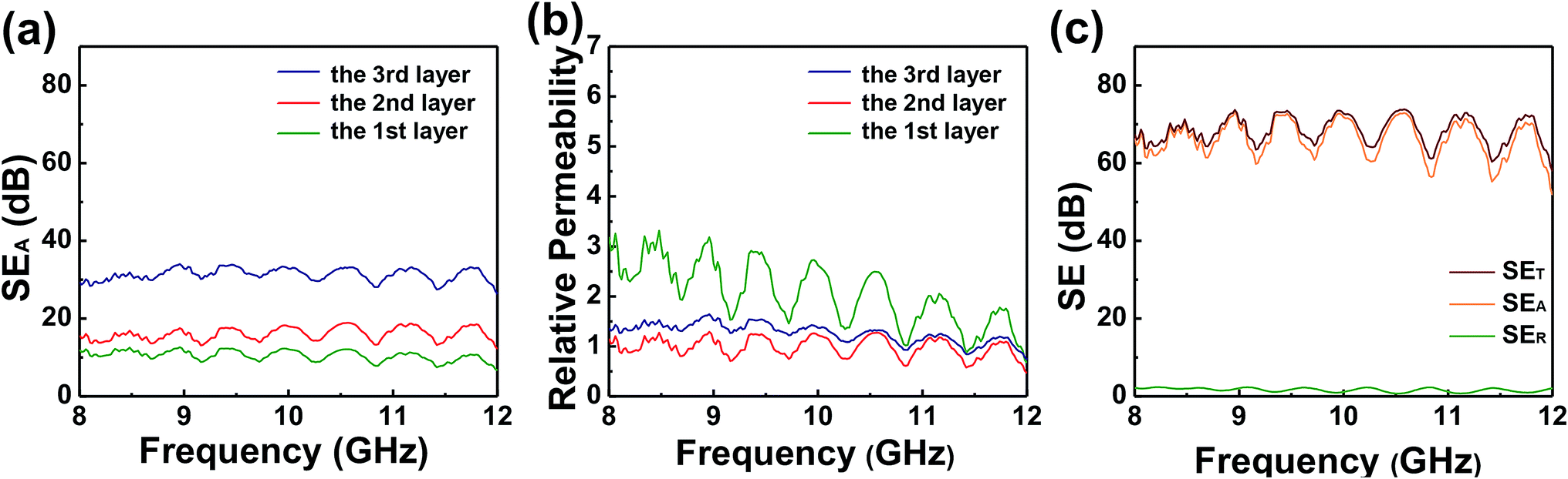 | ||
| Fig. 3 (a) SEA and (b) relative permeability of each layer in the multilayered GNP/Ni/PMMA nanocomposite ({20 wt% GNP/Ni}/{30 wt% GNP/Ni}/{40 wt% GNP/Ni}). (c) Calculation results for SER, SEA and SET of the multilayered GNP/Ni/PMMA nanocomposite. | ||
Since the conductivities of all layers are higher than 2πfε0 at 8 and 12 GHz (0.445 and 0.668, see Table S1†), the skin depth was calculated using eqn (10).
When a wave is incident from the air to the surface of a conductive material, if Z02 » Z1, where Z0 (Z02 = μ0/ε0) and Z1 (Z12 = 2πfμ1/σ1) is the impedance of air and that of the 1st layer, the SER of the multilayered structure can be written as eqn (11).32
 | (11) |
The reflection between the n − 1th and nth layer inside the mutilayered structure is presented by the following eqn (12),
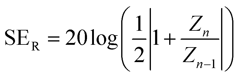 | (12) |
 | (13) |
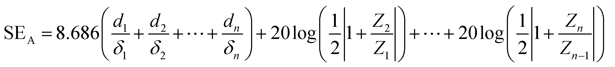
SEA consists of absorption terms of each layer and reflection terms between layers with different GNP/Ni concentrations. The value of SEA is a function of the thickness of the material as well as the electrical conductivity and the permeability. Since each layer has the same thickness, the conductivity and magnetic permeability are variables in SEA.
The calculation of SET, SER and SEA of the mutilayered GNP/Ni/PMMA nanocomposite ({20 wt% GNP/Ni}/{30 wt% GNP/Ni}/{40 wt% GNP/Ni}) was carried out using the eqn (5), (11) and (13), respectively. Fig. 3(c) shows the calculated values of SER, SEA and SET of the mutilayered structure. The investigation of the EMI shielding mechanism demonstrates that the most part of the incident wave is absorbed after it penetrates the material due to the high impedance of the 1st layer, inducing a decrease in SER. Once the incident wave propagates into layers, it is attenuated by conductive dissipation and extra internal reflection between layers. It contributes to SEA, which constitutes the largest part of SET.
The experimental results shown in Fig. 2 and the calculation results were compared to investigate whether the shielding properties of the mutilayered structure match with a theoretical mechanism. Fig. 4 shows the theoretical and experimental results for SER, SEA and SET of the multilayered GNP/Ni/PMMA nanocomposite shown in Fig. 1(b). According to the results, SE due to absorption is much higher than that due to reflection; this demonstrates that absorption is the major shielding mechanism in the multilayered GNP/Ni/PMMA nanocomposite. Therefore, the multilayered system shows SET of 54–85 dB, which is 1585 times that of the monolayered system (22–26 dB, see Fig. 2(c)). Once the incident wave is applied on a material, absorption inside the whole material can dominantly affect the EMI shielding properties as a result of the absorption of each layer and internal reflection between layers.
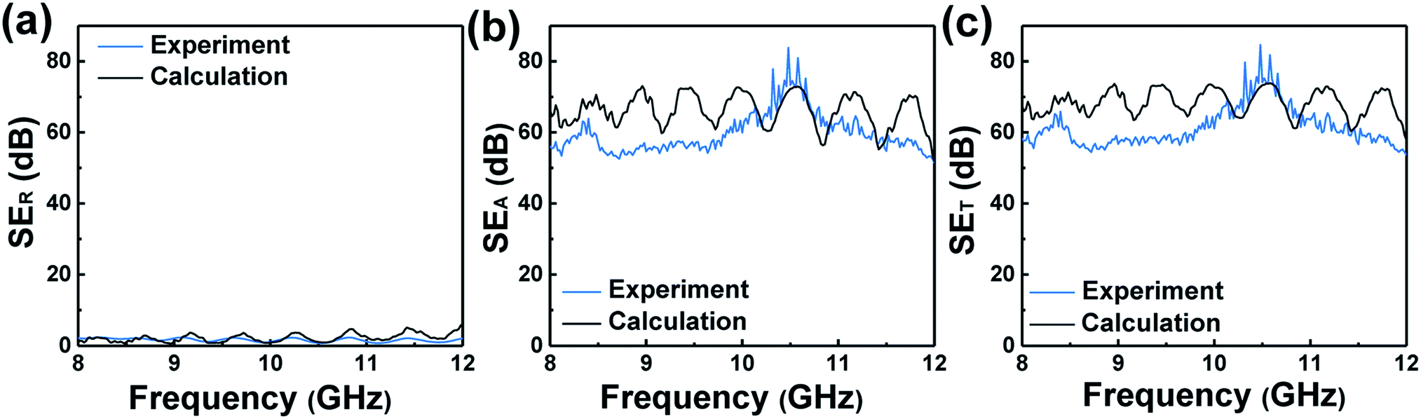 | ||
| Fig. 4 Theoretical and experimental results for the multilayered GNP/Ni/PMMA nanocomposite ({20 wt% GNP/Ni}/{30 wt% GNP/Ni}/{40 wt% GNP/Ni}); (a) SER, (b) SEA and (c) SET. | ||
In addition, the two peaks shown in Fig. 4(b) and (c) are responsible for resonance absorption due to the effects of mutilayered structure and the thickness.9 The increase in absorption results from the cancellation of wave reflected from the surface of the material and at the rear surface. Therefore, SET increases in the designated range of frequency.
Fig. 5 shows the EMI shielding properties of the recently reported graphene/nanoparticle/polymer and multilayered nanocomposite materials in the X-band region. Various EMI shielding structures have been reported using graphene/nanoparticle/polymer system to increase internal reflection inside a material. Despite of various EMI shielding structures reported in the recent literature, multilayered system using GNP, Ni nanoparticle and PMMA can take advantages of easy fabrication process, which are favorable from an engineering point-of-view.
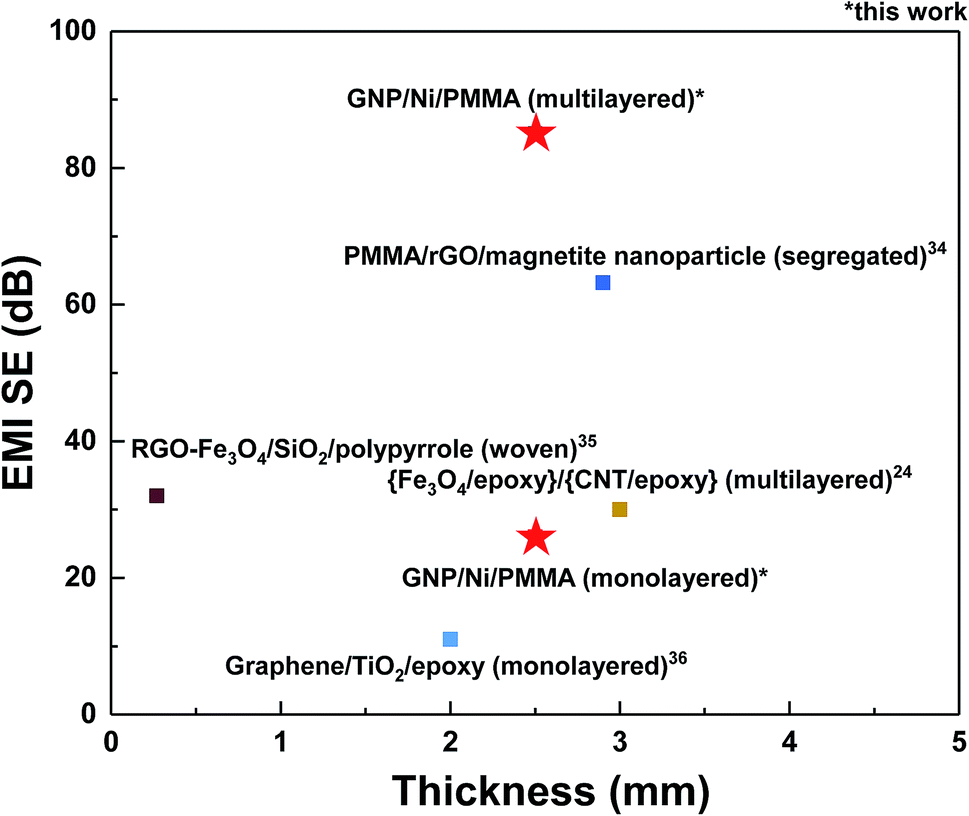 | ||
| Fig. 5 EMI shielding properties of the recently reported graphene/nanoparticle/polymer nanocomposite materials with various structures. | ||
4. Conclusions
Herein, multilayered GNP/Ni/PMMA nanocomposites ({20 wt% GNP/Ni}/{30 wt% GNP/Ni}/{40 wt% GNP/Ni}) and monolayered GNP/Ni/PMMA nanocomposites {30 wt% GNP/Ni} were fabricated with the objective of maximizing the EMI shielding properties of the GNP/Ni nanocomposite at a given amount in a matrix. Multilayered nanocomposites were designed by increasing the GNP/Ni weight fraction by 10 wt% between the contacting layers; this led to an abrupt increase in the conductivity along the wave propagation direction. Their SE were measured and compared in terms of the contribution of multilayered structures to EMI shielding. Furthermore, the theoretical and experimental results of the multilayered structure show similar trends; this makes it possible to investigate the EMI shielding mechanism. The main factors responsible for the enhancement of the shielding capability of the multilayered nanocomposites were the increase in the absorption and reflection capabilities of the 2nd and 3rd layers and additional reflection. Moreover, reflection from the surface of the material could be minimized by increasing the impedance of the 1st layer. Therefore, our studies on multilayered nanocomposites using GNP/Ni in the polymer matrix can be exploited for designing improved EMI shielding material where their thickness and amount of conductive fillers are limited. This system can maximize the EMI shielding properties by inducing additional internal reflections that result from abrupt impedance changes. This strategy can be applied to various scales and kinds of material.Conflicts of interest
There are no conflicts to declare.Acknowledgements
This work was supported by the Nano·Material Technology Development Program through the National Research Foundation of Korea (NRF) funded by the Ministry of Science, ICT and Future Planning [grant number 2016M3A7B4905609].References
- J. Liang, Y. Wang, Y. Huang, Y. Ma, Z. Liu, J. Cai, C. Zhang, H. Gao and Y. Chen, Carbon, 2009, 47, 922–925 CrossRef CAS.
- P. C. P. Watts, W.-K. Hsu, A. Barnes and B. Chambers, Adv. Mater., 2003, 15, 600–603 CrossRef CAS.
- S. Ryu, C. B. Mo, H. Lee and S. H. Hong, J. Nanosci. Nanotechnol., 2013, 13, 7669–7674 CrossRef CAS PubMed.
- Y. Li, X. Pei, B. Shen, W. Zhai, L. Zhang and W. Zheng, RSC Adv., 2015, 5, 24342–24351 RSC.
- W.-L. Song, L.-Z. Fan, M.-S. Cao, M.-M. Lu, C.-Y. Wang, J. Wang, T.-T. Chen, Y. Li, Z.-L. Hou, J. Liu and Y.-P. Sun, J. Mater. Chem. C, 2014, 2, 5057–5064 RSC.
- V. Eswaraiah, V. Sankaranarayanan and S. Ramaprabhu, Macromol. Mater. Eng., 2011, 296, 894–898 CrossRef CAS.
- A. P. Singh, M. Mishra, D. P. Hashim, T. N. Narayanan, M. G. Hahm, P. Kumar, J. Dwivedi, G. Kedawat, A. Gupta, B. P. Singh, A. Chandra, R. Vajtai, S. K. Dhawan, P. M. Ajayan and B. K. Gupta, Carbon, 2015, 85, 79–88 CrossRef CAS.
- M. Verma, P. Verma, S. K. Dhawan and V. Choudhary, RSC Adv., 2015, 5, 97349–97358 RSC.
- M. Verma, A. P. Singh, P. Sambyal, B. P. Singh, S. K. Dhawan and V. Choudhary, Phys. Chem. Chem. Phys., 2015, 17, 1610–1618 RSC.
- S. Kim, J. Oh, M. Kim, W. Jang, M. Wang, Y. Kim, H. W. Seo, Y. C. Kim, J. Lee, Y. Lee and J. Nam, ACS Appl. Mater. Interfaces, 2014, 6, 17647–17653 CrossRef CAS PubMed.
- S. K. Hong, K. Y. Kim, T. Y. Kim, J. H. Kim, S. W. Park, J. H. Kim and B. J. Cho, Nanotechnology, 2012, 23, 455704 CrossRef PubMed.
- W. Li, D. Li, Q. Fu and C. Pan, RSC Adv., 2015, 5, 80428–80433 RSC.
- Y. Tong, S. Bohm and M. Song, Austin J. Nanomed. Nanotechnol., 2014, 1, 1003 Search PubMed.
- D. A. C. Brownson and C. E. Banks, Phys. Chem. Chem. Phys., 2012, 14, 8264–8281 RSC.
- H. J. Im, G. H. Jun, D. J. Lee, H. J. Ryu and S. H. Hong, J. Mater. Chem. C, 2017, 5, 6471–6479 RSC.
- S. Stankovich, D. A. Dikin, R. D. Piner, K. A. Kohlhaas, A. Kleinhammes, Y. Jia, Y. Wu, S. T. Nguyen and R. S. Ruoff, Carbon, 2007, 45, 1558–1565 CrossRef CAS.
- Z. Wang, J. Luo and G. Zhao, AIP Adv., 2014, 4, 017139 CrossRef.
- J. Hwang, T. Yoon, S. H. Jin, J. Lee, T.-S. Kim, S. H. Hong and S. Jeon, Adv. Mater., 2013, 25, 6724–6729 CrossRef CAS PubMed.
- J. R. Potts, D. R. Dreyer, C. W. Bielawski and R. S. Ruoff, Polymer, 2011, 52, 5–25 CrossRef CAS.
- H. B. Zhang, Q. Yan, W. G. Zheng, Z. He and Z. Z. Yu, ACS Appl. Mater. Interfaces, 2011, 3, 918–924 CrossRef CAS PubMed.
- S.-T. Hsiao, C.-C. M. Ma, H.-W. Tien, W.-H. Liao, Y.-S. Wang, S.-M. Li, C.-Y. Yang, S.-C. Lin and R.-B. Yang, ACS Appl. Mater. Interfaces, 2015, 7, 2817–2826 CrossRef CAS PubMed.
- S. Stankovich, D. A. Dikin, G. H. B. Dommett, K. M. Kohlhaas, E. J. Zimney, E. A. Stach, R. D. Piner, S. T. Nguyen and R. S. Ruoff, Nature, 2006, 442, 282–286 CrossRef CAS PubMed.
- M. Chen, Y. Zhu, Y. Pan, H. Kou, H. Xu and J. Guo, Mater. Des., 2011, 32, 3013–3016 CrossRef CAS.
- Y. Liu, D. Song, C. Wu and J. Leng, Composites, Part B, 2014, 63, 34–40 CrossRef CAS.
- L. Q. Zhang, B. Yang, J. Teng, J. Lei, D. X. Yan, G. J. Zhong and Z. M. Li, J. Mater. Chem. C, 2017, 5, 3130–3138 RSC.
- N. F. Colaneri and L. W. Shacklette, IEEE Trans. Instrum. Meas., 1992, 41, 291–297 CrossRef.
- A. Joshi, A. Bajaj, R. Singh, A. Anand, P. S. Alegaonkar and S. Datar, Composites, Part B, 2015, 69, 472–477 CrossRef CAS.
- Y. Chen, Y. Li, M. Yip and N. Tai, Compos. Sci. Technol., 2013, 80, 80–86 CrossRef CAS.
- Y. Xu, Y. Yang, D. X. Yan, H. Duan, G. Zhao and Y. Liu, ACS Appl. Mater. Interfaces, 2018, 10, 19143–19152 CrossRef CAS PubMed.
- B. R. Schulz, V. C. Plzntz and D. R. Brush, IEEE Trans. Electromagn. Compat., 1988, 30, 187–201 Search PubMed.
- L. Vovchenko, Y. Perets, I. Ovsienko, L. Matzui, V. Oliynyk and V. Launetz, Surf. Coat. Technol., 2012, 211, 196–199 CrossRef CAS.
- W. L. Song, M. S. Cao, M. M. Lu, S. Bi, C. Y. Wang, J. Liu, J. Yuan and L. Z. Fan, Carbon, 2014, 66, 67–76 CrossRef CAS.
- M. H. Al-Saleh and U. Sundararaj, Carbon, 2009, 47, 1738–1746 CrossRef CAS.
- F. Sharif, M. Arjmand, A. A. Moud, U. Sundararaj and E. P. L. Roberts, ACS Appl. Mater. Interfaces, 2017, 9, 14171–14179 CrossRef CAS PubMed.
- Y. Yuan, W. Yin, M. Yang, F. Xu, X. Zhao, J. Li, Q. Peng, X. He, S. Du and Y. Li, Carbon, 2018, 130, 59–68 CrossRef CAS.
- A. Kumar, R. Anant, K. Kumar, S. S. Chauhan, S. Kumar and R. Kumar, RSC Adv., 2016, 6, 113405 RSC.
Footnote |
| † Electronic supplementary information (ESI) available. See DOI: 10.1039/c9ra00573k |
| This journal is © The Royal Society of Chemistry 2019 |