
 Open Access Article
 This Open Access Article is licensed under a Creative Commons Attribution-Non Commercial 3.0 Unported Licence
Annealing effects on the structural and dielectric properties of (Nb + In) co-doped rutile TiO2 ceramics
Lanling Zhao ad,
Jun Wangb,
Zhigang Gaia,
Jichao Lia,
Jian Liua,
Jiyang Wangc,
Chunlei Wang*a and
Xiaolin Wang*d
ad,
Jun Wangb,
Zhigang Gaia,
Jichao Lia,
Jian Liua,
Jiyang Wangc,
Chunlei Wang*a and
Xiaolin Wang*d
aSchool of Physics, State Key Laboratory of Crystal Materials, Shandong University, Jinan, Shandong 250100, P. R. China. E-mail: wangcl@sdu.edu.cn
bKey Laboratory for Liquid-Solid Structural Evolution and Processing of Materials, Shandong University, Jinan, Shandong 250061, P. R. China
cInstitute for Crystal Materials, Shandong University, Jinan, 250100, P. R. China
dInstitute for Superconducting and Electronic Materials, University of Wollongong, NSW 2500, Australia. E-mail: xiaolin@uow.edu.au
First published on 14th March 2019
Abstract
Density functional theory calculations were conducted to investigate the electronic structures of rutile Ti16O32, Ti13Nb2InO32, and Ti13Nb2InO31 systems. High density (Nb + In) co-doped rutile TiO2 ceramics were successfully prepared by one modified solid state method. XRD, XPS, Raman scattering and FT-IR measurements were performed to investigate the structural properties of the (Nb + In) co-doped rutile TiO2 ceramics annealed in different atmospheres. The lattice parameters for the (Nb + In) co-doped rutile TiO2 ceramics were enlarged slightly after they were annealed in air and oxygen. Raman scattering results indicate that the Eg modes are quite sensitive to oxygen vacancy in comparison with the other Raman active modes. The ceramics annealed in oxygen at 873 K exhibit the best dielectric performance with giant dielectric permittivity (>14![[thin space (1/6-em)]](https://www.rsc.org/images/entities/char_2009.gif) 000) and small dielectric loss (<0.2) over the frequency range from 40 Hz to 1 MHz.
000) and small dielectric loss (<0.2) over the frequency range from 40 Hz to 1 MHz.
1. Introduction
Recently, dielectric materials with colossal permittivity (CP, >104) and sufficiently low dielectric loss are attracting great attention motivated by the increasing demands owing to the miniaturization and multi-functionality of apparatus used in high charge-storage capacitors and high speed integrated circuits.1–3 Several kinds of materials with giant dielectric permittivity have been proposed, for instance, BaTiO3-doped perovskite,4 CaCu3Ti4O12 (ref. 5) and rock salt-type Li0.05Ti0.02Ni0.93O.6 However, none of them has demonstrated a colossal dielectric permittivity and quite low dielectric loss over a broad frequency range so far. So it is urgent to find such a material that possesses giant dielectric permittivity, quite small dielectric loss and can be used in many application areas such as in super capacitors and energy storage. According to the Variational Density Functional Perturbation Theory, rutile TiO2 can possess unusually large static dielectric permittivity.7 Since Hu et al.8 reported the excellent dielectric performance of (Nb + In) co-doped TiO2 ceramics in 2013, great attention has been drawn to the TiO2-based giant dielectric materials thanks to its elemental abundance and low toxicity in recent years.3,9–12It should be noted that both the intrinsic and extrinsic factors could affect the excellent dielectric performance of TiO2-based ceramics. Several mechanisms have been proposed and developed to describe this excellent dielectric response. Hu et al.8 considered that the highly localized electron-pinned defect dipoles favorite the colossal permittivity and low dielectric loss in (Nb + In) co-doped TiO2 ceramics, which is known as the EPDD model. Li et al.13 proposed a model of internal barrier layer capacitance, known as the IBLC model, to explain the excellent dielectric performance in (Nb + In) co-doped TiO2 ceramics. In addition, the surface barrier layer capacitor (SBLC) effect and non-ohmic sample-electrode contact have also been reported to contribute to the colossal dielectric response in (Nb + In) co-doped TiO2 ceramics.14,15
In this work, we report (Nb + In) co-doped TiO2 ceramics with giant dielectric permittivity and small dielectric loss over the frequency range from 40 Hz to 1 MHz. High density ceramics were prepared by one modified solid state method. To understand how the doped elements and annealing conditions affect the dielectric properties of the TiO2 system, the electronic structures for the pure and (Nb + In) co-doped rutile TiO2 were studied by conducting related density functional theory (DFT) calculations. XRD, XPS, Raman scattering and FT-IR measurements were performed to investigate the structural properties of oxygen deficient (Nb + In) co-doped rutile TiO2 ceramics. The results indicate that annealing in air and oxygen leads to the lattice parameters enlarged slightly and the Raman active Eg modes are quite sensitive to oxygen defects. The ceramics annealed in oxygen at 873 K exhibit giant dielectric permittivity (>14000) and small dielectric loss (<0.2) over the frequency range from 40 Hz to 1 MHz.
2. Experimental and calculation details
The raw materials used in this work are Anatase TiO2 (99.8%, Sigma Aldrich), Nb2O5 (99.9%, Sigma Aldrich) and In2O3 (99.999%, Sigma Aldrich) which are heated in oven at 423 K for 4 hours to completely remove any absorbed water. The ceramics were prepared in a rubber hose and then pressed by using hydrostatic press system. The ceramics were heated to 1773 K at a rate of 2 K min−1 for 10 h followed by cooling down to room temperature naturally. Disk ceramics with the same thickness were cut from the rod. In order to investigate the effects of oxygen defects on the structural and dielectric properties, some of the obtained ceramics were annealed in air for 72 h at 873 K, and some samples were annealed in oxygen for 72 h at the same temperature.Phase analysis of as-prepared (Nb + In) co-doped rutile TiO2 ceramics was performed in the 2-theta range from 2° to 90° by using a GBC MMA X-ray diffraction instrument. Raman scattering experiments were applied to obtain additional information on the internal atom vibrations of as-prepared samples by using a JOBIN YVON HR800 Confocal Raman system with the 632.8 nm He–Ne laser. The laser was focused on the sample powders through a microscope equipped with a ×100 objective. Fourier Transformed Infrared (FT-IR) spectra of sample powders were recorded using the KBr method in the range 400–1500 cm−1. The samples were prepared by grinding a mixture of the sample powders and KBr powders in an agate mortar and then pressing them in the usual way. X-ray photoelectron spectroscopy (XPS) is conducted using a SPECS PHOIBOS 100 Analyzer installed in a high-vacuum chamber with the base pressure below 10−8 mbar, X-ray excitation was provided by Al Kα radiation with photon energy hν = 1486.6 eV at the high voltage of 12 kV and power of 120 W. The XPS binding energy spectra were recorded at the pass energy of 20 eV in the fixed analyzer transmission mode. Analysis of the XPS data was carried out by using the commercial Casa XPS 2.3.15 software package. To construct parallel-plate Pt/TiO2/Pt capacitors, the Pt electrodes (99.99%) were coated by a sputter coater (Edwards sputter coater AUTO 306) in vacuum around 2.00 × 10⁻³ mbar at room temperature. The dielectric behaviour was studied using an Agilent 4294A Impedance Analyzer from 40 Hz to 1 MHz at room temperature in air ambience.
DFT calculations were performed using the Vienna Ab initio Simulation Package (VASP),16,17 with the ionic potentials including the effect of core electrons being described by the projector augmented wave (PAW) method.18,19 A plane-wave energy cutoff of 400 eV is used in all calculations. All structures are geometrically relaxed until the total force on each ion was reduced to be less than 0.01 eV A−1. Heyd, Scuseria and Ernzerhof (HSE) hybrid functional20 is used in the electronic band structures and density-of-states calculations.
3. Results and discussion
Fig. 1a–c shows the XRD patterns for the as-prepared (Nb + In) co-doped TiO2 ceramics, which indicates that all samples show the same crystal structure as rutile structured TiO2 with slightly changed lattice parameters. Specifically, compared to the un-annealed sample, the air-annealed sample and oxygen-annealed sample show much larger lattice parameters due to less oxygen defects. Fig. 1d shows the calculated electronic band structures and density of states for stoichiometric rutile TiO2, revealing that the stoichiometric rutile TiO2 exhibits an indirect electronic band gap around 3.1 eV with the conduction band extrema at M point and valance band extrema at Γ point, which is in good agreement with the experimental value of 3.0 eV. Fig. 1e–f shows the differential charge density distributions of Ti16O32, Ti13Nb2InO32, and Ti13Nb2InO31 compounds. It indicates that the oxygen defects as well as the dopants of indium and niobium could lead to the charge redistributed in rutile TiO2 particularly near the dopants and oxygen vacancies. Specifically, the introduction of niobium leads to delocalized electrons, while the introduction of indium yields obvious localized electrons and oxygen vacancy holds back the delocalized electron caused by niobium doping. According to the EPDD model, the highly localized electron-pinned defect dipoles caused by the introduction of indium and niobium could benefit the dielectric performance of the rutile TiO2. Therefore, the redistributed charge could affect the dielectric properties of this system.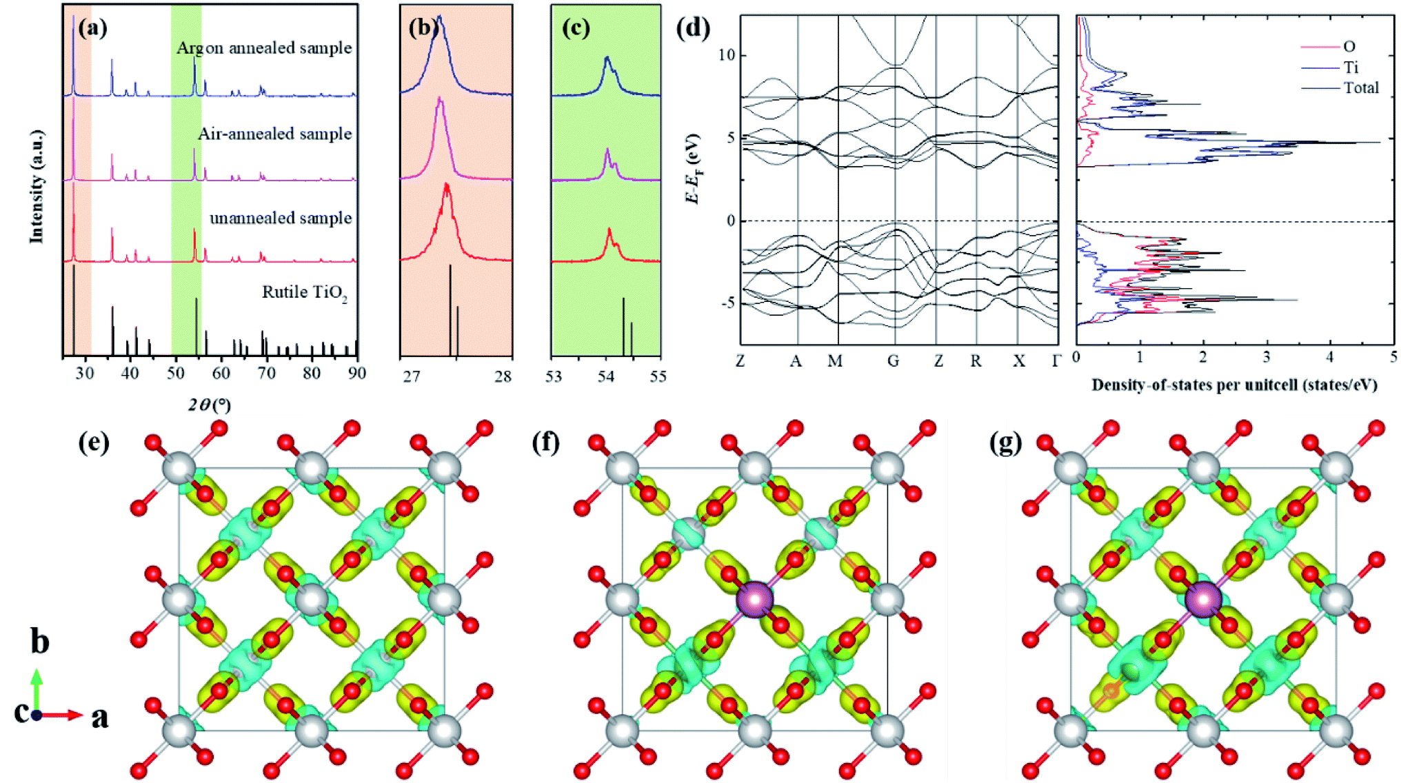 | ||
| Fig. 1 (a–c) XRD patterns for the as-prepared (Nb + In) co-doped TiO2 ceramics; (d) calculated electronic band structures and density-of-states for stoichiometric rutile TiO2; (e and f) differential charge density distributions of Ti16O32, Ti13Nb2InO32, and Ti13Nb2InO31 compounds. Yellow and blue colors indicate the positive and negative values of electron quantities, respectively. The isosurface value is set to 0.02. Red, grey, purple and blue spheres refer to oxygen, titanium, indium and niobium atoms, respectively. | ||
Rutile structured TiO2 belongs to P42/mnm space group with two formula units in one primitive cell. According to group theory, its optical phonon irreducible representation can be given by the following formula,
| Γopt = A1g + A2g + A2u + 2B1u + B1g + B2g + Eg + 3Eu | (1) |
All E modes are two-fold degenerate. The A2u, B1u and Eu modes are IR active, whereas the B1g, Eg, A1g and B2g modes are Raman active which are normally located at around 143 cm−1, 447 cm−1, 612 cm−1 and 826 cm−1, respectively.21–23 And the A2g modes are Raman inactive. Four first-order Raman active modes and one second-order modes located at about 238 cm−1 were present in the Raman spectra of as-prepared rutile TiO2 samples and their corresponding eigenvectors were displayed in Fig. 2. Obvious red-shift of the Eg modes (447 cm−1) can be observed after the annealing process compared to the other Raman active modes. It can be ascribed that Eg modes are related to the libration motion of the oxygen atoms along the C4 axis, while B1g, B2g and A1g modes are all Ti–O stretch or breathing modes24 which can be found from the Raman active mode's eigenvectors shown in Fig. 2a. Therefore, the Eg modes are more sensitive to oxygen defects than the other Raman active modes.
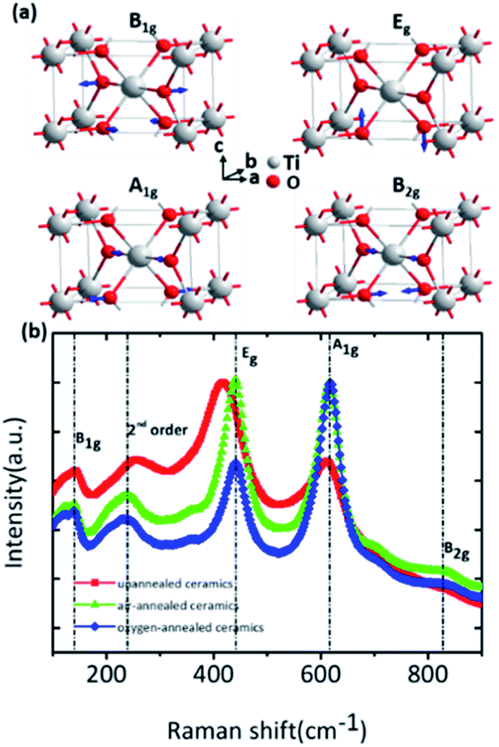 | ||
| Fig. 2 (a) Raman active modes' eigenvectors of rutile TiO2 (the sizes of eigenvectors have been enlarged to clarify the movements of atoms); (b) Raman spectra of as-prepared (Nb + In) co-doped rutile TiO2 ceramics. | ||
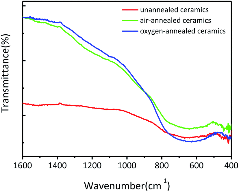
Fig. 3 shows the FT-IR transmittance spectra of the obtained (Nb + In) co-doped TiO2 ceramics. All ceramics show a broad band located at 500–800 cm−1 which can be ascribed to the characteristic vibrations of the Ti–O–Ti network structure.25–28 Specifically, compared to the un-annealed ceramics, the oxygen-annealed and air-annealed ceramics exhibit sharper peaks thanks to the intensified Ti–O–Ti bonds leaded by the less oxygen vacancies in ceramics.
 | ||
| Fig. 3 FT-IR spectra of the obtained (Nb + In) co-doped TiO2 ceramics. | ||
Fig. 4i provides the survey spectra and high resolution Ti 2p, O 1s, Nb 3d and In 3d core level spectra of as-prepared ceramics. It is indicated that In an Nb are successfully incorporated into rutile TiO2 crystal lattice. Fig. 4ii shows the characteristic 2p3/2 and 2p1/2 spin doublet from Ti4+ located at 458.69 and 464.15 eV, respectively, with a peak separation of 5.46 eV. The O 1s region (Fig. 4iii) was composed of two peaks located at about 530.9 and 531.7 eV corresponding to the two different Ti–O bonds (bond length: 1.9818 Å and 1.9412 Å, respectively) existed in the rutile TiO2. Two characteristic peaks of 3d5/2 and 3d3/2 were present in the high resolution Nb 3d and In 3d core level spectra (Fig. 4iv and v) which indicated the presence of In3+ and Nb5+ in all samples. For the prepared ceramics, it is indicated that all peaks in the core level spectra of oxygen-annealed samples shifted to higher energy compared to the other samples. It is related to the less oxygen defects in ceramics.
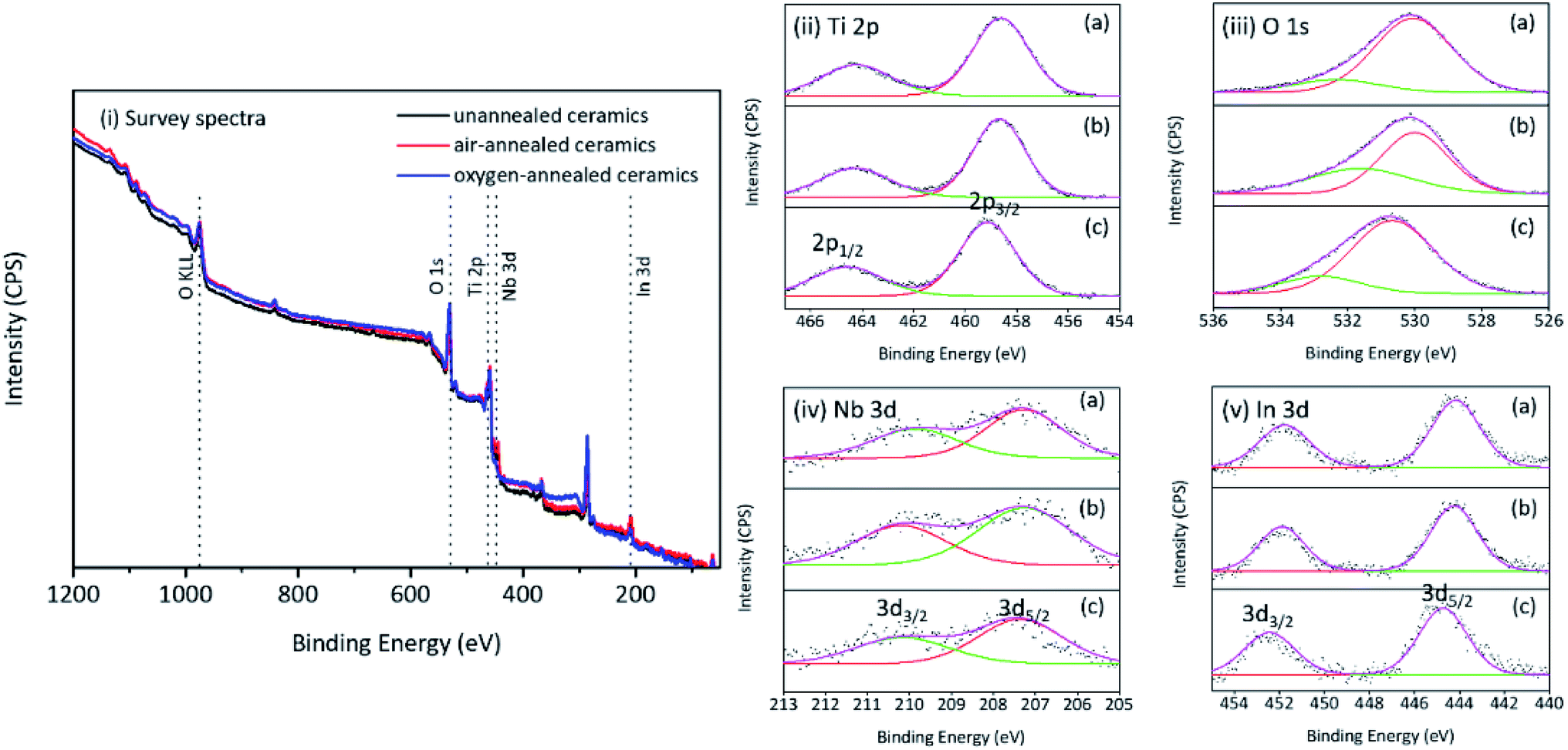 | ||
| Fig. 4 (i) XPS survey spectra of as-prepared (Nb + In) co-doped TiO2 ceramics, (ii) the XPS spectra of Ti 2p band, (iii) the XPS spectra of O 1s band, (iv) The XPS spectra of In 3d band, (v) the XPS spectra of Nb 3d band for un-annealed ceramics (a), air-annealed ceramics (b) and oxygen-annealed ceramics (c). | ||
Fig. 5 shows the frequency dependence of dielectric permittivity and dielectric loss of (Nb + In) co-doped rutile TiO2 ceramics at room temperature. All ceramics exhibit slowly decreased dielectric permittivity with increased frequency. The dielectric loss for un-annealed ceramics was as high as 50 at 40 Hz and then sharply decreased to around 0.2 when the frequency is higher than 0.05 MHz. The air-annealed and oxygen-annealed ceramics show less frequency dependent dielectric loss with values around 0.2 in the whole measured frequency range. Compared to the un-annealed and air-annealed ceramics, the oxygen-annealed ceramics show higher dielectric permittivity ranging from 1.4 × 10⁴ to 3.0 × 10⁴ over the frequency range from 40 Hz to 1 MHz. It should be noted that the air-annealed ceramics exhibit the lowest dielectric permittivity among all ceramics and comparable dielectric loss with the oxygen-annealed ceramics in the measured frequency range. Furthermore, the dielectric performance of the air-annealed and oxygen-annealed ceramics was almost unchanged after polishing followed by recoating Pt electrodes, indicating that the oxygen entered the ceramics and became stable during the long-time annealing process. The complicated air and oxygen annealing effects on the dielectric performance of the (Nb + In) co-doped rutile TiO2 ceramics prove that it is hard to clearly point out which mechanism is the main reason for the excellent dielectric performance of rutile TiO2-based ceramics. Not only the localized electron-pinned defect dipoles but also the internal barrier layer capacitance could benefit the dielectric performance.
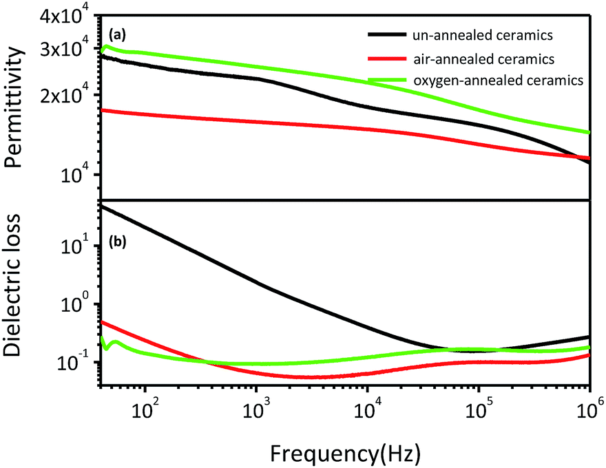 | ||
| Fig. 5 Room temperature frequency dependence of dielectric permittivity (a) and dielectric loss (b) for (Nb + In) co-doped rutile TiO2 ceramics. | ||
4. Conclusions
DFT calculations using the HSE hybrid functional confirmed that the stoichiometric rutile TiO2 exhibits an indirect electronic band gap around 3.1 eV, which is in good agreement with the experimental value of 3.0 eV. After annealed in air or oxygen, both the structural and dielectric properties of the as-prepared ceramics exhibited much difference. The lattice parameters were enlarged slightly and became more and more close to the theoretical values which can be confirmed by the Raman results. FT-IR results further proved that all samples are rutile structured TiO2 and XPS results give evidence of Nb and In doped in samples successfully. The ceramics annealed in oxygen showed larger dielectric permittivity (>14000) and smaller dielectric loss (<0.2) in the frequency range from 40 Hz to 1 MHz compared to the others.
Conflicts of interest
There are no conflicts to declare.Acknowledgements
L. L. Z. thanks the support from the Fundamental Research Funds of Shandong University (2016HW003) and the China Postdoctoral Science Foundation (2017M622198). J. W. is grateful for the support from the Fundamental Research Funds of Shandong University (2016HW004). Z. G. G. is grateful for the support from the Natural Science Foundation of Shandong Province (ZR2013EMM018).Notes and references
- Z.-M. Dang, Y.-H. Lin and C.-W. Nan, Adv. Mater., 2003, 15, 1625–1629 CrossRef CAS
.
- C. Huang, Q. M. Zhang and J. Su, Appl. Phys. Lett., 2003, 82, 3502–3504 CrossRef CAS
- X. Zhu, L. Yang, J. Li, L. Jin, L. Wang, X. Wei, Z. Xu and F. Li, Ceram. Int., 2017, 43, 6403–6409 CrossRef CAS
- L. Wu, X. Wang and L. Li, J. Alloys Compd., 2016, 688, 113–121 CrossRef CAS
- C. C. Homes, T. Vogt, S. M. Shapiro, S. Wakimoto and A. P. Ramirez, Science, 2001, 293, 673–676 CrossRef CAS PubMed
- J. Wu, C. W. Nan, Y. Lin and Y. Deng, Phys. Rev. Lett., 2002, 89, 217601 CrossRef PubMed
- C. Lee and X. Gonze, Phys. Rev. B, 1994, 49, 14730–14731 CrossRef CAS
- W. Hu, Y. Liu, R. L. Withers, T. J. Frankcombe, L. Noren, A. Snashall, M. Kitchin, P. Smith, B. Gong, H. Chen, J. Schiemer, F. Brink and J. Wong-Leung, Nat. Mater., 2013, 12, 821–826 CrossRef CAS PubMed
- Y. Yu, W.-L. Li, Y. Zhao, T.-D. Zhang, R.-X. Song, Y.-L. Zhang, Z.-Y. Wang and W.-D. Fei, J. Eur. Ceram. Soc., 2018, 38, 1576–1582 CrossRef CAS
- X.-g. Zhao and P. Liu, J. Alloys Compd., 2017, 715, 170–175 CrossRef CAS
- K. Tsuji, H. Han, S. Guillemet-Fritsch and C. A. Randall, Phys. Chem. Chem. Phys., 2017, 19, 8568–8574 RSC
- H. Taniguchi, K. Ando and I. Terasaki, Jpn. J. Appl. Phys., 2017, 56, 10PC02 CrossRef
- J. Li, F. Li, Y. Zhuang, L. Jin, L. Wang, X. Wei, Z. Xu and S. Zhang, J. Appl. Phys., 2014, 116, 074105 CrossRef
- T. Nachaithong, P. Thongbai and S. Maensiri, J. Eur. Ceram. Soc., 2017, 37, 655–660 CrossRef CAS
- Y. Q. Wu, X. Zhao, J. L. Zhang, W. B. Su and J. Liu, Appl. Phys. Lett., 2015, 107, 242904 CrossRef
- G. Kresse and J. Hafner, Phys. Rev. B: Condens. Matter Mater. Phys., 1993, 47, 558 CrossRef CAS
- G. Kresse and J. Hafner, Phys. Rev. B: Condens. Matter Mater. Phys., 1994, 49, 14251 CrossRef CAS
- P. E. Blochl, Phys. Rev. B: Condens. Matter Mater. Phys., 1994, 50, 17593 CrossRef
- G. Kresse and D. Joubert, Phys. Rev. B: Condens. Matter Mater. Phys., 1999, 59, 1758 CrossRef CAS
- S. Heyd, G. E. Scuseria and M. Ernzerhof, J. Chem. Phys., 2003, 118, 8207 CrossRef
- R. J. Betsch, H. L. Park and W. B. White, Mater. Res. Bull., 1991, 26, 613–622 CrossRef CAS
- S. P. S. Porto, P. A. Fleury and T. C. Damen, Phys. Rev., 1967, 154, 522–526 CrossRef CAS
- A. Orendorz, A. Brodyanski, J. Lösch, L. H. Bai, Z. H. Chen, Y. K. Le, C. Ziegler and H. Gnaser, Phys. Status Solidi C, 2007, 4, 1822–1829 CrossRef CAS
- J. C. Parker and R. W. Siegel, J. Mater. Res., 1990, 5, 1246–1252 CrossRef CAS
- N. Mir and M. Salavati-Niasari, Electrochim. Acta, 2013, 102, 274–281 CrossRef CAS
- X. Xue, Y. Wang and H. Yang, Appl. Surf. Sci., 2013, 264, 94–99 CrossRef CAS
- M. Hamadanian, A. Reisi-Vanani and A. Majedi, Appl. Surf. Sci., 2010, 256, 1837–1844 CrossRef CAS
- T. Tong, J. Zhang, B. Tian, F. Chen and D. He, Mater. Lett., 2008, 62, 2970–2972 CrossRef CAS
| This journal is © The Royal Society of Chemistry 2019 |