
 Open Access Article
 This Open Access Article is licensed under a Creative Commons Attribution-Non Commercial 3.0 Unported Licence
Thin layer broadband porous chromium black absorber fabricated through wet-etching process
Lang Zhou ab,
Zhuo Liab,
Jinying Zhangab,
Defang Liab,
Dan Liuab,
Yajie Liab and
Xin Wang*ab
ab,
Zhuo Liab,
Jinying Zhangab,
Defang Liab,
Dan Liuab,
Yajie Liab and
Xin Wang*ab
aSchool of Optics and Photonics, Beijing Institute of Technology, Beijing 100081, P. R. China. E-mail: wangxin@bit.edu.cn
bBeijing Key Lab for Precision Optoelectronic Measurement Instrument and Technology, China
First published on 10th May 2019
Abstract
A thin layer porous chromium (Cr) black absorber was fabricated on a polyimide (PI) substrate with 2 inch diameter and 500 nm thickness. The chromium black was prepared by electron beam evaporation and wet-etching process. To optimize the parameters of the absorber, the Cr black was firstly fabricated on silicon and quartz wafers. A high average absorption of 93% over the whole visible spectrum (320 nm to 800 nm) was obtained by 3 min wet-etching of a 400 nm thick metal Cr film. The absorption was higher than 65% when the spectrum extended to near infrared from 800 to 1800 nm. The mechanism of the ultra-broadband absorption can be explained by the light trapping by numerous nanovoids formed inside the Cr film. The nanovoid acts as a blackbody cavity, where the incident light experienced multiple reflections. Using the optimized parameters obtained with silicon and quartz wafers, the Cr black absorber was fabricated on a PI film. Due to its porous structure (low density) and thin thickness, the Cr black/PI composite film showed a strong light absorption and a high optical thermal response. Compared to a PI film without Cr black layer, the average absorption of the composite film was increased from 5.0% to 93.4%, the optical thermal response was improved by 43.5 times. This property highlights its potential applications in various fields such as photo detection and thermal imaging.
1 Introduction
Owing to their high mechanical strength, good thermal stability, low dielectric constant and good flexibility, polyimide (PI) films are attractive for many applications, including microelectronics, medicine, aerospace engineering and fuel cells.1–5 Good transparency of PI is preferable when it is used in displays,6,7 light-emitting diodes8 and window coatings.9,10 However, the low absorption of pure PI severely limits its applications in thermal emitters, sensors, and thermal imagers, where high optical–thermal response is required,11–13 i.e. the material need to have high absorption of light and fast thermal response. To increase the optical absorption of PI film and at the same time keep its flexibility, a thin layer black absorber that can be fabricated on PI film is desired.Numerous broadband absorbers have been proposed in the past decades. The most typical designs include periodic electric ring resonators, tapered nanocones and porous metal coatings. For periodic electric ring resonators and metal–insulator–metal cavities, the central wavelength of the absorption band could be designed from microwave to visible.14–16 But the absorption bandwidth is usually narrow due to their intrinsic wave resonance. To extend the absorption spectral bandwidth, multi-order mode17,18 or multiple resonators19–22 had to be designed. The sophisticated nanofabrication procedures hindered their mass production for practical applications, especially when the desired absorption wavelength is in the visible spectrum.19 To achieve broadband and angle insensitive absorption, nickel-phosphorus absorber with 5 μm-depth etched pores23,24 and vertically aligned carbon nanotube arrays with the thicknesses varied in the range of 10–800 μm![[thin space (1/6-em)]](https://www.rsc.org/images/entities/char_2009.gif) 25–27 were fabricated. The high broadband absorption is brought by the multiple reflection inside the nanostructures. Among different nanostructures, nanocone with rough surface is proved to be the most efficient. Various absorbers based on nanocones, such as black silicon28–30 and metallic nanocone arrays31–33 were fabricated. Their broadband absorption is higher than 99%. But these kind of thick (tens of micrometers) and heavy absorbers are not suitable to be used on soft polymer films. Otherwise, the flexibility and thermal properties of thin PI films would be totally changed. Loosely porous gold black34 and aluminium black35 not only have broadband absorption but also can be fabricated on thin polymer films. However, the adhesion on the substrates is not strong due to both the metal crystal structures and the heat evaporation coating technology. In addition, because of their mechanical fragility36 the gold or aluminium black coatings are easily broken when there is a force or a temperature change.
25–27 were fabricated. The high broadband absorption is brought by the multiple reflection inside the nanostructures. Among different nanostructures, nanocone with rough surface is proved to be the most efficient. Various absorbers based on nanocones, such as black silicon28–30 and metallic nanocone arrays31–33 were fabricated. Their broadband absorption is higher than 99%. But these kind of thick (tens of micrometers) and heavy absorbers are not suitable to be used on soft polymer films. Otherwise, the flexibility and thermal properties of thin PI films would be totally changed. Loosely porous gold black34 and aluminium black35 not only have broadband absorption but also can be fabricated on thin polymer films. However, the adhesion on the substrates is not strong due to both the metal crystal structures and the heat evaporation coating technology. In addition, because of their mechanical fragility36 the gold or aluminium black coatings are easily broken when there is a force or a temperature change.
In this paper, a thin porous Cr black absorber with no more than 400 nm thickness is fabricated on a 500 nm thick free-standing PI film. Compared to gold and aluminium, Cr film shows better adhesion to silicon, oxide glass and polymer substrates.37,38 A dense metal Cr film was deposited by electro-beam evaporation on substrate, which ensured good adhesion, uniformity and mechanical strength. Micro- and nano-voids were formed on the Cr thin film via wet-etching with Cr corrosive solution. The size of the micro- and nano-voids and the absorption could be controlled by wet-etching parameters.
To get the optimized fabrication parameters, a number of Cr black absorber samples were fabricated on Si and quartz wafers. The samples made on Si substrate were used for crystal structure, film morphology, optical reflection from ultraviolet-visible (UV-VIS) to near infrared (NIR) range and NIR range transmission measurements. The samples made on quartz substrate were used for UV-VIS range transmission measurement. With 3 min wet-etching of a 400 nm thick metal Cr film, the Cr black absorber showed an average absorption as high as 93% covering a wide spectrum from 320 nm to 800 nm. Finally, by using the optimized parameter we obtained from Si and quartz wafers, the high absorption Cr black absorber was fabricated on a 500 nm-thick PI film with 2 inch diameter. Compared to a bare PI film, the average absorption was increased from 5% to 93.4%, the optical thermal response of the Cr black/PI composite film had a 43.5 times enhancement. In addition, compared to absorbers based on periodic electric ring resonators and nanocones, the deposition/wet-etching process is easier to accomplish, more efficient and low-cost, which makes mass production possible.
2 Experimental section
2.1. Material
One side polished Si (100) and quartz wafers (500 μm thickness, 2 inch diameter, Tianjin semiconductor research institute) were used as substrates for Cr black absorber sample fabrication. Cr particles (99.95% purity, 3 to 5 mm diameter, ZNXC technology co., LTD, China) were used for metal Cr film preparation. Ammonium ceric nitrate (NH4)2Ce(NO3)6 powder (99.0%, Macklin), glacial acetic acid (36%, Macklin) and distilled water were used to produce corrosive solution for Cr wet-etching.SiO2 (300 nm)/Si (500 μm) wafer (2 inch diameter, Tianjin semiconductor research institute) was used as substrates for free-standing Cr black/PI composite film fabrication. Liquid poly(amic acid) (PAA) solution with the viscosity of 300–400 cps (25 °C) and the solid content of 12–13% (ZKPI-305IIB, POME technology) was used as the PI precursor. Hydrofluoride acid (40%, Macklin) was used to wet-etch SiO2 sacrificial layer.
2.2. Preparation of Cr black absorber samples
Cr absorbers samples were prepared on Si (100) or quartz wafers. The wafers were soaked in a 100 °C piranha solution (3 parts H2SO4 to 1 part 30 wt% H2O2 by volume) for 15 min and then thoroughly rinsed with distilled water for wet-chemical cleaning. After that, high purity Cr particles with the diameter of 3 to 5 mm were used to deposit metal Cr film on the cleaned wafers by electron-beam evaporating at 5 × 10⁻⁶ Torr (NEXDEP, Angstrom Engineering). The wafer temperature was 110 °C and the evaporation rate was 0.1 nm s−1. The thickness of Cr films was monitored in situ by a quartz crystal oscillator and further calibrated by step profiler. A Cr metal film with 400 nm thickness was deposited on wafers.The wafers with Cr metal film were cut into 2 cm × 4 cm small samples, then dipped into Cr corrosive solution for wet-etching. Cr corrosive solution was prepared by 25 g (NH4)2Ce(NO3)6 powder, 20 ml glacial acetic acid and 100 ml distilled water. The solution temperature was kept at 20 °C. The metal Cr films was wet-etched through the following chemistry reaction:
| (NH4)2Ce(NO3)6 + Cr → Cr(NO3)2 + Ce(NO3)2 + 2NH4NO3+ H2O | (1) |
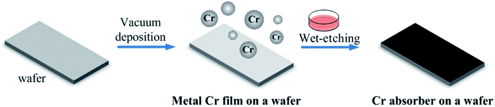 | ||
| Fig. 1 The overall procedure to prepare Cr black absorbers on Si or quartz substrates. | ||
2.3. Preparation of the free-standing Cr black/PI composite film
The Cr black/PI free-standing film fabrication began with the wet-chemical cleaning of 2 inch SiO2 (300 nm)/Si (500 μm) thermal oxide wafers. PAA solution was used as the PI precursor. To enhance the adhesion between PAA layer and SiO2, the wafer was surface modified in Ar–O2 atmosphere for 2 min. The radio-frequency (RF) power was 100 W (GIGAbatch 310M, PVA TePla AG). The gas flows of Ar and O2 were 20 sccm and 100 sccm, respectively. 6 ml PAA solution was spin-coated on the SiO2 layer at the low speed of 800 rpm for 1 min, then followed by the high speed of 4000 rpm for 3 min (LabSpin6, SUSS MicroTec). The PAA coating was then air-dried at room temperature for 1 h, and cured in a high temperature oven filled with nitrogen gas with temperatures increasing steps at 100, 200, 250 and 300 °C (1 h at each temperature). After that, the PAA coating was cooled naturally from 300 °C to room temperature. The formation of PI was verified by its particular canary yellow color, as a thin transparent film. The thickness of the PI film was measured by a surfagauge (Surftest SJ-140, Mitutoyo). Using the above process parameters, a PI film with the thickness of 500 nm was made. To overlay a Cr black absorber on PI film, a 400 nm metal Cr film was vacuum deposited on PI film first, then the film was wet-etched for 3 min to form the optimized porous Cr black structure. Prior to delamination process, the stress of the Cr black/PI composite film was dispersed on a 500 °C hot plate for 1 h. To make the Cr black/PI composite film free-standing, the SiO2 sacrificial layer was removed completely by wet-etching in hydrofluoride acid solution for 10 min. So that, the 2 inch black/PI composite film peeled off from the Si substrate totally and floated over the surface of solution. In the end, the composite film was transferred gently and supported by a PI ring. The overall procedure to prepare the free-standing Cr black/PI composite film was presented schematically in Fig. 2.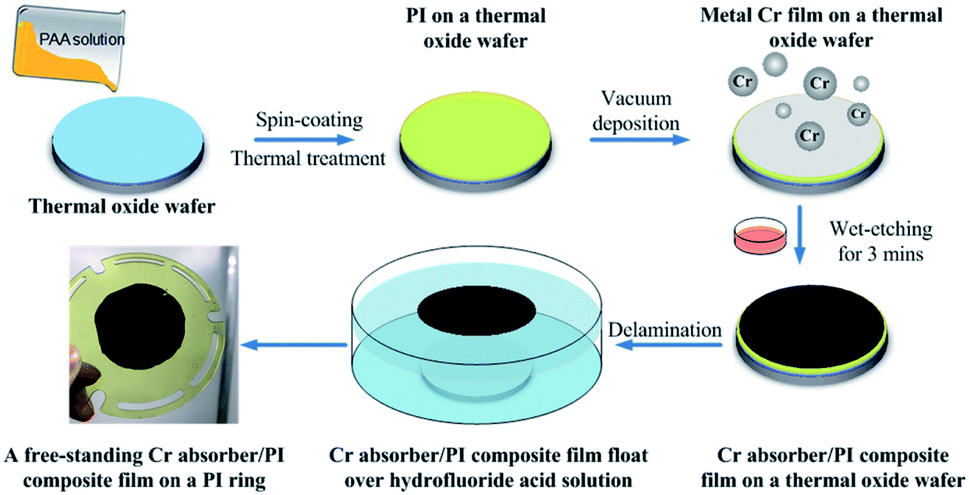 | ||
| Fig. 2 The overall procedure to prepare the free-standing Cr black/PI composite film. | ||
2.4. Characterization methods
X-ray diffraction (XRD) patterns of the metal Cr film and Cr black absorber samples on Si substrate were acquired using Cu-Kα radiation (λ = 0.15418 nm), at an accelerating voltage of 40 kV and current of 40 mA (Rigaku Ultima IV). The detailed surface morphologies of the metal Cr film and Cr black absorber samples on Si substrate were characterized by field emission scanning electron microscopy (FE-SEM, Zeiss SUPRA™ 55 SAPPHIRE) and atomic force microscopy (AFM, Multimode8, BRUKER). Integrated reflectance and transmittance spectra of Cr absorbers in the range of 320–1800 nm were obtained by a PerkinElmer Lambda 19 spectrometer with an integration sphere. The light incident angle was 0°. The light sources were a tungsten halogen and a deuterium lamp, the detectors were photomultiplier and lead sulfide detector for UV-VIS and NIR, respectively. In reflectance measurement, the sample substrate was Si. In transmittance measurement, the sample substrates were quartz in UV/VIS region and Si in NIR region, respectively, to obtain good light transparency. For the reflectance measurement the results were normalized to a Labsphere Spectralon reflectance standard.To deduce the absorption of the Cr black absorber the transmittances of both the samples and the substrates were measured. According to the sample transmittance expression25
| Tsample ≈ TCr × Tsubstrate | (2) |
Assuming the light reflected by the substrate to the Cr black absorber is either absorbed or passed through the Cr black absorber; as illustrated in Fig. 3. Due to the low transmittance of Cr film, the light energy reflected by substrate was as low as ∼4‰, which was negligible. Thus, Rsample (reflectance of the samples) was determined mainly by RCr (reflectance of the black absorbers). The integrated absorption of the Cr black absorber (ACr) could be calculated by the following relations between absorption, reflection and transmission:
| Asample ≈ 1 − RCr − Tsample | (3-1) |
| ACr ≈ 1 − RCr − TCr | (3-2) |
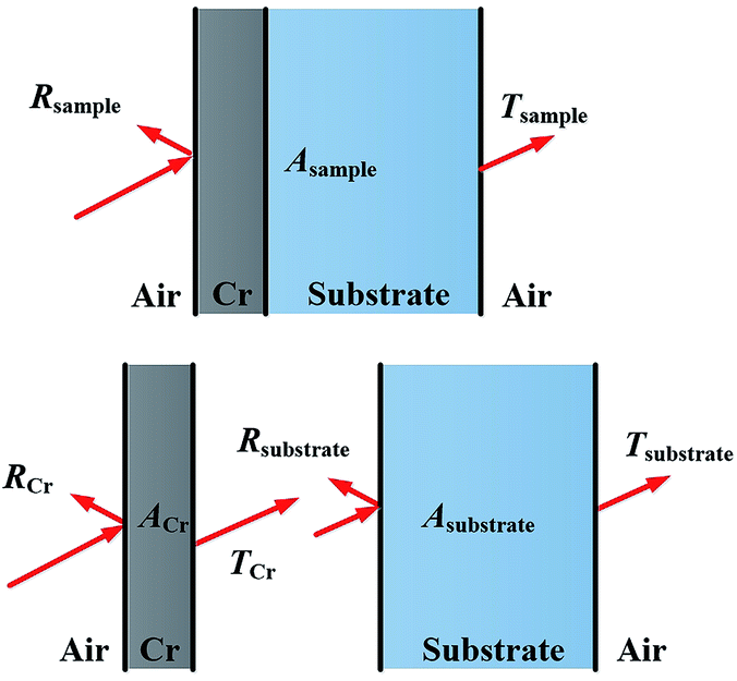 | ||
| Fig. 3 Illustration of the absorption calculations of the Cr black absorbers. | ||
The optical thermal responses and thermal decay time of a Cr black/PI composite film were investigated. The measurement schematic is shown in Fig. 4. An intensity modulated solid-state laser operating at 532 nm wavelength was used as an exciting light source. The modulation frequency was 5 Hz and duty cycle was 50%. The laser peak power was 1.2 W. The diameter of the laser beam was 20 mm. The film was placed in a vacuum chamber with pressure of 1 × 10⁻⁶ Torr to decrease the heat convection. The vacuum chamber has two optical windows. One is a fused quartz window with antireflection coating from 350 nm to 800 nm spectrum for visible light transmission, the other is a germanium window with antireflection coating from 3 μm to 5 μm spectrum for middle wave infrared (MWIR) transmission. The laser beam incident normally to the surface of the sample through the fused quartz window. By absorbing the light, the temperature of the Cr black/PI composite film changed according to the laser intensity modulation. Thus, a modulated thermal radiation was observed. The radiation was collected by optics and directed to a MWIR photo detector (PD) through the germanium window. The output signal of the PD is sampled by a digital oscilloscope for further analysis.
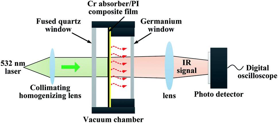 | ||
| Fig. 4 The measurement schematic of optical thermal responses and thermal decay time. | ||
3 Results and discussion
3.1. Morphology
Fig. 5 shows the crystal quality of a 400 nm metal Cr film and 3 min wet-etching Cr black absorber sample. The strong peak of Si (substrate) was not shown in this figure. The strong and sharp peak near 2θ = 44.4° corresponds to the Cr (110) crystal orientation, shown in Fig. 2(a). The full width at half maximum (FWHM) of the curve is 0.6°. Based on the Bragg diffraction angle and the FWHM of the diffraction pattern in the 2θ scan, the average grain size of the metal Cr film is estimated to be 13 nm by Debye–Scherrer formula. Meanwhile, the diffraction peaks at 2θ = 64.6° (200) and 81.7° (211) are hardly to be observed due to the thin thickness of Cr film. During wet-etching process, Cr atoms gradually reacted with (NH4)2Ce(NO3)6 in acid environment. The products, Cr(NO3)2 and Ce(NO3)2 were completely dissolved in solution. Thus, a porous Cr film was formed by randomly spatial atom lost. The forming process was improved by the 3 min wet-etching sample scan, shown in Fig. 2(b), where the intensity of the Cr (110) peak decreased and the FWHM of the curve became broaden. In addition, no new peak is observed. The result indicates that there is no new byproduct contained by porous Cr black absorbers from the wet-etching chemical reaction. The observed grey and black appearance were due to the light-trapping of porous Cr nanostructures, as shown in SEM images of Fig. 6.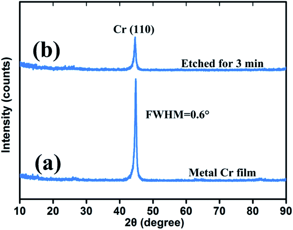 | ||
| Fig. 5 XRD measurement results of metal Cr film and Cr black absorber on Si substrates. | ||
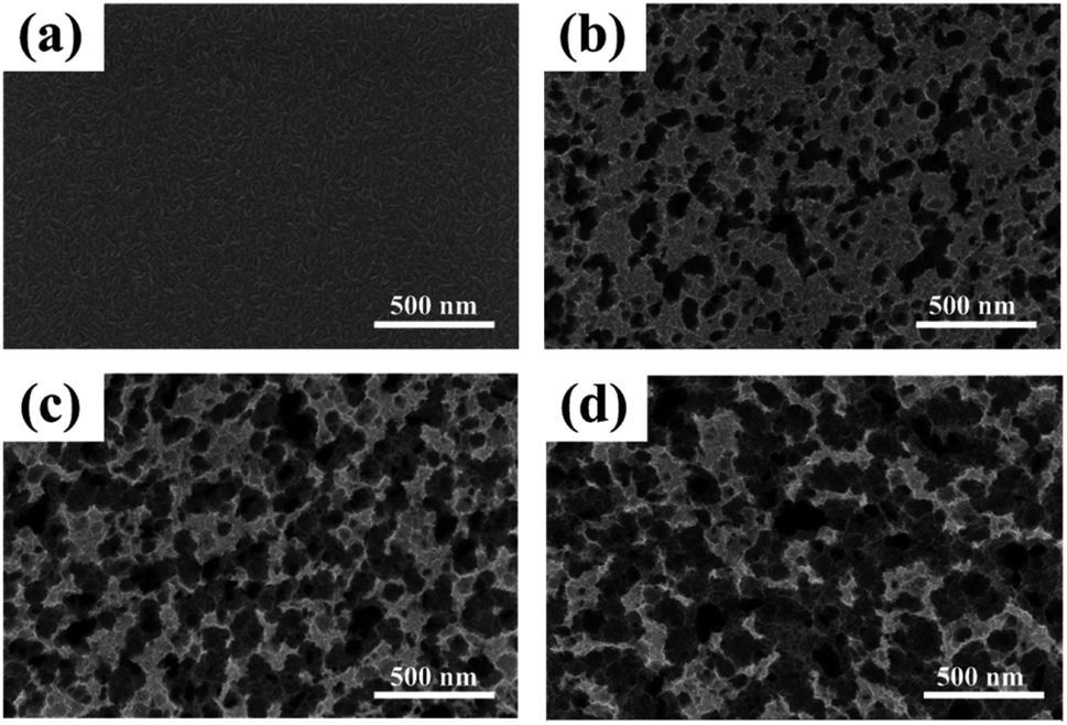 | ||
| Fig. 6 FE-SEM images of metal Cr film and Cr black absorbers on Si substrate with different wet-etching times. (a) Metal Cr film, (b) etched for 2 min, (c) etched for 3 min, (d) etched for 4 min. | ||
Fig. 6 shows the surface morphologies of metal Cr film and Cr black absorber samples with different wet-etching times. Surface details were further investigated by AFM, as shown in Fig. 7. For 400 nm metal Cr film without wet-etching, the root mean square (RMS) of the surface roughness is 3.9 nm within a 5 μm × 5 μm area; the surface fluctuation from peak to valley is 17 nm; as shown in Fig. 7(a)–(c). It indicates that the surface of the metal Cr film is smooth and shows specular reflection. After 2 min etching (Fig. 6(b)), innumerable voids (black region) appeared. The Cr cluster diameter is tens of nanometers. These voids form innumerable black body cavities, to capture and absorb the incident light. As the etching time increasing, the black voids became deeper and bigger. After 3 min wet-etching, voids were connected to each other, resulting in the formation of voids with the big average diameter of 200 nm, as shown in Fig. 6(c). Observed by AFM, the RMS of the Cr layer surface increases to 50.5 nm and the largest surface fluctuation from peak to valley is up to 240 nm, as shown in Fig. 7(f). After 4 min, the voids were destroyed and parts of Si substrate were exposed, as in Fig. 6(d). After 7–8 min, the metal Cr film was corroded completely.
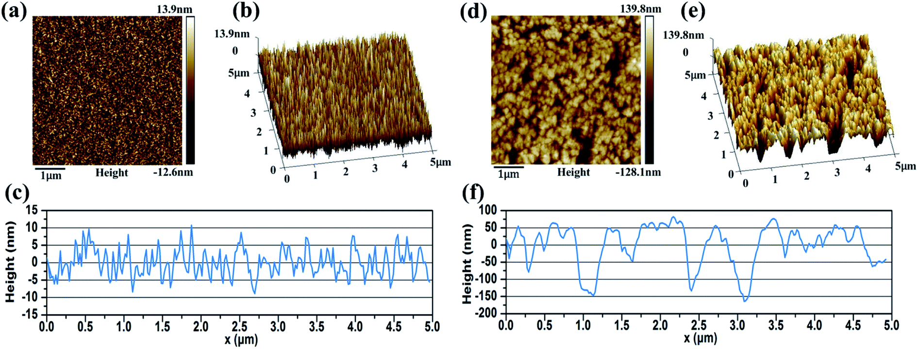 | ||
| Fig. 7 (a) The top-view AFM image, (b) three-dimensional AFM image and (c) surface fluctuation profile of 400 nm metal Cr film on Si substrate; (d) the top-view AFM image, (e) three-dimensional AFM image and (f) surface fluctuation profile of Cr black absorber on Si substrate etched for 3 min. | ||
3.2. Optical properties
To investigate the light absorption properties of Cr black absorbers, the transmission and reflection of the Cr black absorber samples were measured. For transmission measurements, the substrate has to be transparent in certain spectral range. Therefore, the Cr black absorber samples fabricated on quartz were used in the transmission measurements in UV-VIS region (from 320 nm to 1100 nm). In the spectral range of 1100 nm to 1800 nm, Si substrate was used instead. Fig. 8 is the photo of the Cr black absorber samples with 0, 2, 3, 4 min wet-etching, respectively. The metal Cr layer has a silvery metallic appearance. In comparison, the Cr black film fabricated with 3 min wet-etching time has a matted black, glossy appearance. Fig. 8 shows the reflectance and colour changes at different wet-etching times.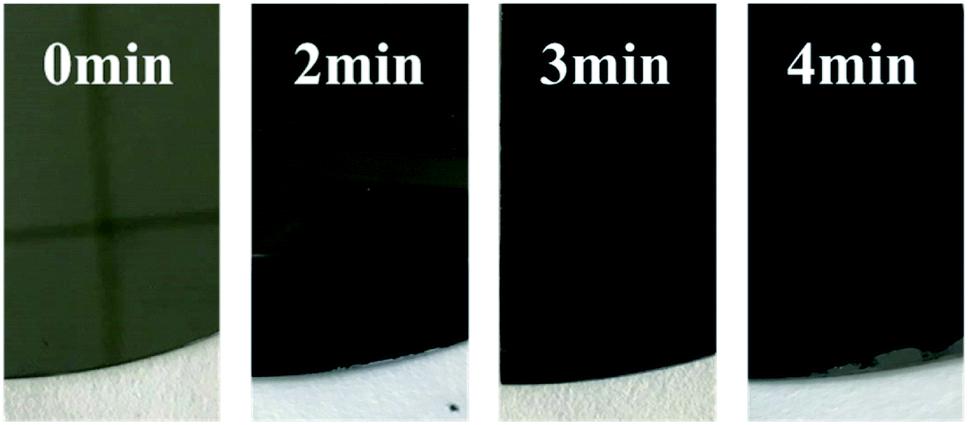 | ||
| Fig. 8 Photographs of metal Cr films and Cr black absorbers with different wet-etching time on Si (100) substrate. | ||
The transmission spectra of 3 min etched Cr black absorber samples on Si and quartz were shown in Fig. 9(a) by black squares and red dots, respectively. With the known transmittances of the substrates, the transmission spectrum of Cr black absorber from 320 nm to 1800 nm was calculated by formula (2).
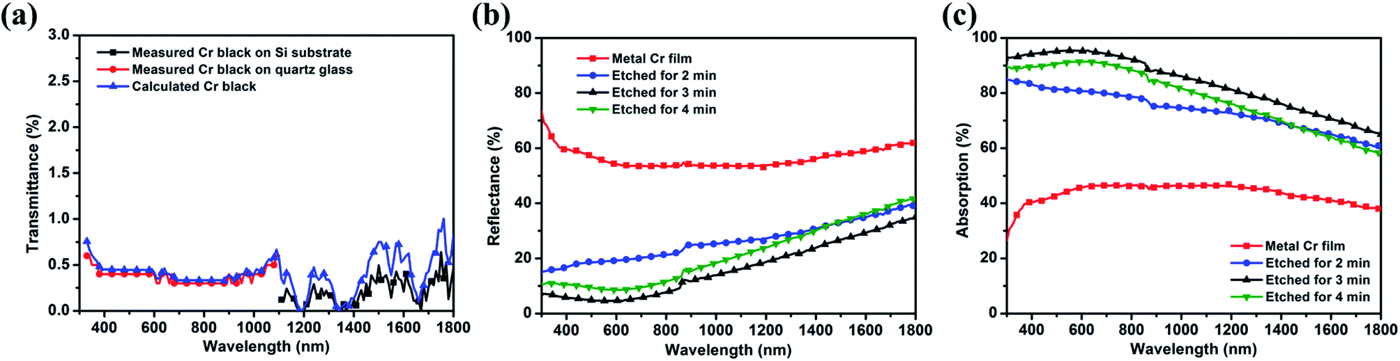 | ||
| Fig. 9 (a) Transmission spectra of the Cr black absorber samples on quartz glass and Si substrate for 3 min wet-etching and the calculated transmission spectrum of the Cr black absorber. (b) Reflectance spectra of metal Cr film and Cr black absorbers on Si substrates with different wet-etching times. (c) Calculated absorption spectra of metal Cr film and Cr black absorbers with different wet-etching times. | ||
Fig. 9(b) is the reflectance measurement results of the Cr black absorber samples on Si substrate, with different wet-etching times. It indicates that the rougher the absorber surface is, the lower reflectance it has.
With the results shown in Fig. 9(a) and (b), the integrated absorption (ACr) spectra of Cr black absorbers were calculated by formula (3-2). The calculation results are shown in Fig. 9(c). The dithering at 860 nm is due to grating switching of the spectrometer. The average absorption of metal Cr film is about 46% in the range of 600 nm to 1300 nm and decreases in the UV and NIR regions. This absorption can be correlated with the free electron oscillation of Cr atoms with the incident light. After 2 min etching, the average absorption dramatically increases to 80% in visible range, indicating the formation of porous nanostructures. When the etching time is up to 3 min, the average absorption exceeds 93% from 320 nm to 800 nm, and the highest absorption is up to 95% at 530 nm. To extend to the NIR region, the absorption decreases linearly from 93% to 65% with a slope of −0.02% nm−1. These phenomenon could be correlated with the large imaginary part of Cr permittivity.39 The incident light energy dissipates rapidly along the large rough Cr surface within a short propagation distance, resulting in a high optical absorption. In addition, Cr nanovoids with gradual diameter variations in a wide range make the impedance match well with free space in a broad wavelength range, which significantly reduces the surface reflection and enhances absorption.31 The decreased absorption at 4 min etching time is due to the reduction of film thickness and voids destruction, as shown in Fig. 6(d).
Since Spectralon delivers a constant reflectance of 99% from 300 nm to about 1600 nm, and even lower reflectance at higher wavelengths (1750–2500 nm),40,41 the systematic error of the reflectance measurements is considered to be 1%. In addition, the impurities and scratches of the optical components will reduce the Spectralon's reflectance, leading to an underestimation of the sample absorption by at least 2% of the measured value.
Using the corrected absorption of the Cr black absorber with 3 min wet-etching, the average absorption coefficients αλ is calculated by
| ACr = 1 − exp(−αλd) | (4) |
3.3. Optical thermal response
In this section, the optical–thermal response of the free-standing Cr black/PI composite film with a diameter of 2 inch is investigated. The Cr black absorber was made by 3 min wet-etching of a 400 nm thick metal Cr film and the thickness of the PI was 500 nm. Ref. 42 gives an average absorption of 5% for pure PI thin film in UV-VIS.42 Using the result in Fig. 9(c), the absorption of the Cr black/PI composite film would be 93.4%. Fig. 10(a) shows the normalized thermal radiation intensities of Cr black/PI composite film and bare PI film under the same incident light excitation. The Cr black/PI composite film shows a much higher optical thermal responsibility, while the bare PI film had very weak thermal radiation due to low absorption at 532 nm. By thermal radiation intensity normalization, the maximum radiation intensities of the Cr black/PI composite film and the bare PI film are 1 and 0.023, respectively. An enhancement of the optical thermal responsibility of 43.5 times was obtained.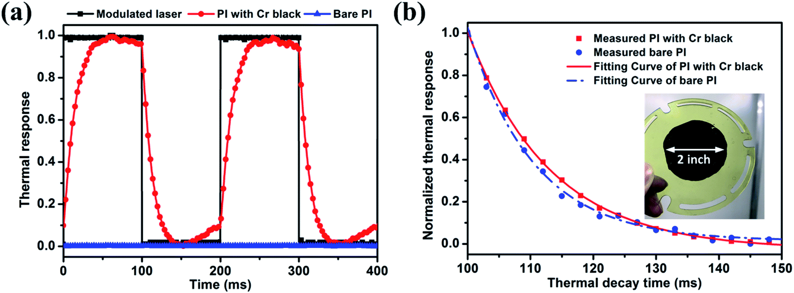 | ||
| Fig. 10 (a) Optical thermal response of Cr black/PI composite film and bare PI film under a 5 Hz intensity modulated 532 nm laser excitation. (b) Thermal decay of composite film and bare PI film. The inset in (b) is a 2 inch free-standing Cr black/PI composite film. | ||
The thermal decay curves are shown in Fig. 10(b) and were fitted by
| ΔI = exp(t0 − t)/τ | (5) |
Based on the working mechanization, if the Cr black absorbers with shorter wet-etching times are used, the optical thermal responsibility will decrease and the thermal decay time will increase. That is induced by the lower light absorption and higher mass density.
In conclusion, by using the Cr black absorber the high optical thermal conversion efficiency can be obtained without sacrificing the time response.
4 Conclusions
In summary, a simple and low-cost method to produce broadband porous Cr black absorber was proposed. By metal Cr film deposition and subsequent chemical wet-etching, an absorber with the thickness of no more than 400 nm was fabricated. The average absorption was higher than 93% in the range of 320–800 nm and the absorption peak located at 530 nm. Even extending to the NIR range (800–1800 nm), the absorption was still over 65%. The broadband absorption property could be explained by porous nanostructures inside the Cr black absorber, where light internal multiple reflection happened. The absorption coefficient of the black Cr absorber was as high as 6.6 μm−1. Compared to the μm-thick perfect absorbers, porous thin layer Cr absorber is more suitable for the applications demanding flexibility and quick thermal response. The black Cr absorber was fabricated on a 500 nm free-standing flexible PI thin film with 2 inch diameter. The optical thermal properties of the composite film were investigated. At the same incident laser intensity, the thermal radiation intensity of the composite film was 43.5 times higher than that of bare PI film, while the thermal decay time only increased by 24.7% (from 10.44 ms to 13.02 ms) with nearly doubled thickness. The novel properties and simple, cost-effective fabrication process make the Cr black/PI composite thin film very attractive to be used in optical thermal devices.Conflicts of interest
The authors declare no conflict of interest.Acknowledgements
This work was supported by the National Natural Science Foundation of China (Grant No. 61875011, 61835001, 61741502 and 61704166). Authors are thankful to the Analysis & Testing Center, Micro-fabrication Center and National Key Laboratory of Color Science and Engineering in Beijing Institute of Technology for providing the characterization facility for this study.References
- T. Xiao, X. Fan, D. Fan and Q. Li, Polym. Bull., 2017, 74, 1–15 CrossRef
.
- M. Haruki, J. Tada, K. Tanaka, H. Onishi and Y. Tada, Thermochim. Acta, 2018, 662, 1–7 CrossRef CAS
- T. Stieglitz, H. R. Beutel, M. Schuettler and J. U. Meyer, Biomed. Microdevices, 2000, 2, 283–294 CrossRef
- Y. Jiang, S. Yu, J. Li, L. Jia and C. Wang, Carbon, 2013, 63, 367–375 CrossRef CAS
- Q. Yuan, P. Liu and G. L. Baker, J. Mater. Chem. A, 2015, 3, 3847–3853 RSC
- Y. J. Kim, S. J. Yu and Y. G. Jeong, RSC Adv., 2016, 6, 30106–30114 RSC
- C. Xia, H. Tao, H. Jiang, B. Wei, G. Chen, X. Fang, M. Jin, R. A. Hayes, G. Zhou and L. Shui, Displays, 2015, 37, 79–85 CrossRef
- W. K. Jin, C. R. Sang, Q. H. Vu, J. Y. So, S. M. Lee, N. T. Mai and L. S. Park, Mol. Cryst. Liq. Cryst., 2009, 513, 214–226 CrossRef
- H. S. Jang, K. J. Sang and S. H. Nahm, Carbon, 2011, 49, 111–116 CrossRef CAS
- T. J. Kang, T. Kim, S. M. Seo, Y. J. Park and H. K. Yong, Carbon, 2011, 49, 1087–1093 CrossRef CAS
- I. E. Araci, V. Demir, A. Kropachev, T. Skotheim, R. A. Norwood and N. Peyghambarian, Appl. Phys. Lett., 2010, 97, 041102 CrossRef
- K. Satori, K. Fukuchi, Y. Kurosawa, A. Hongo and N. Takeda, Proc. SPIE, 2001, 4328, 285–294 CrossRef CAS
- Y. Yang, S. Nuo, L. Zhou, C. Xu, H. Wang, L. Zhang, Y. Li and Z. Li, Proc. SPIE, 2015, 9677, 967708 CrossRef
- C. M. Watts, X. Liu and W. J. Padilla, Adv. Mater., 2012, 24, OP98–OP120 CAS
- M. K. Hedayati, M. Javaherirahim, B. Mozooni, R. Abdelaziz, A. Tavassolizadeh, V. S. Chakravadhanula, V. Zaporojtchenko, T. Strunkus, F. Faupel and M. Elbahri, Adv. Mater., 2011, 23, 5409 CrossRef
- J. Z. Hao, Y. Seokho, T. Fatima, D. H. Werner and T. S. Mayer, ACS Nano, 2011, 5, 4641–4647 CrossRef PubMed
- J. A. Bossard, L. Lan, Y. Seokho, L. Liu, D. H. Werner and T. S. Mayer, ACS Nano, 2014, 8, 1517–1524 CrossRef CAS PubMed
- H. Cheng, S. Chen, H. Yang, J. Li, X. An, C. Gu and J. Tian, J. Opt., 2012, 14, 85102–85106 CrossRef
- Z. Liu, X. Liu, S. Huang, P. Pan, J. Chen, G. Liu and G. Gu, ACS Appl. Mater. Interfaces, 2015, 7, 4962–4968 CrossRef CAS PubMed
- Z. Nan, Z. Peiheng, C. Dengmu, W. Xiaolong, X. Jianliang and D. Longjiang, Opt. Lett., 2013, 38, 1125–1127 CrossRef PubMed
- C. W. Chiu, C. W. Cheng, K. T. Lai, M. H. Shih, M. N. Abbas and Y. C. Chang, Opt. Express, 2012, 20, 10376–10381 CrossRef PubMed
- Z. Bingxin, Z. Yanhui, H. Qingzhen, K. Brian, K. Iam-Choon, C. Shufen and H. Tony Jun, Opt. Express, 2011, 19, 15221–15228 CrossRef PubMed
- F. Xing, B. Zhao and W. Shi, Electrochim. Acta, 2013, 100, 157–163 CrossRef CAS
- Y. F. Wang, W. G. Fu, M. Feng and X. W. Cao, Appl. Phys. A: Mater. Sci. Process., 2008, 90, 549–553 CrossRef CAS
- H. Ye, X. J. Wang, W. Lin, C. P. Wong and Z. M. Zhang, Appl. Phys. Lett., 2012, 101, 141909 CrossRef
- H. Shi, J. G. Ok, H. W. Bacc and L. J. Guo, Appl. Phys. Lett., 2011, 99, 207402 Search PubMed
- F. Ren, H. Yu, W. Li, M. Saleem, Z. Tian and P. Ren, RSC Adv., 2014, 4, 14419–14431 RSC
- B. Zheng, W. Wang, G. Jiang and X. Mei, Appl. Phys. B: Lasers Opt., 2016, 122, 180 CrossRef
- J. Gao, M. Raad, B. P. Bowen, R. N. Zuckermann and T. R. Northen, Anal. Chem., 2016, 88, 1625 CrossRef CAS PubMed
- J. Yang, F. Luo, T. S. Kao, X. Li, G. W. Ho, J. Teng, X. Luo and M. Hong, Light: Sci. Appl., 2014, 3, e185 CrossRef CAS
- J. Wang, Y. Liang, P. Huo, D. Wang, J. Tan and T. Xu, Appl. Phys. Lett., 2017, 111, 251102 CrossRef
- F. Peixun, B. Benfeng, L. Jiangyou, J. Dafa, J. Guofan, Z. Hongjun and Z. Minlin, Nano Lett., 2015, 15, 5988–5994 CrossRef PubMed
- T. Ji, L. Peng, Y. Zhu, F. Yang, Y. Cui, X. Wu, L. Liu, S. He, F. Zhu and Y. Hao, Appl. Phys. Lett., 2015, 106, 495–520 Search PubMed
- D. Panjwani, A. Dutta, J. Nath, H. Heinrich and R. E. Peale, J. Appl. Phys., 2015, 118, 154307 CrossRef
- X. Hu, S. Qin, J. Tian and M. Hu, Sol. Energy Mater. Sol. Cells, 1988, 17, 207–215 CrossRef CAS
- D. Panjwani, M. Yesiltas, S. Singh, E. D. Barco, R. E. Peale, C. Hirschmugl and J. Sedlemair, Infrared Phys. Technol., 2014, 66, 1–5 CrossRef CAS
- N. Jiang and J. Silcox, J. Appl. Phys., 2000, 87, 3768–3776 CrossRef CAS
- J. M. Burkstrand, J. Appl. Phys., 1981, 52, 4795–4800 CrossRef CAS
- P. B. Johnson and R. W. Christy, Phys. Rev. B: Solid State, 1974, 9, 5056–5070 CrossRef CAS
- M. Steglich, D. Lehr, S. Ratzsch, T. Käsebier, F. Schrempel, E. B. Kley and A. Tünnermann, Laser Photonics Rev., 2014, 8, L13–L17 CrossRef CAS
- Z. Liu, H. Liu, X. Wang, H. Yang and J. Gao, Sci. Rep., 2017, 7, 42750 CrossRef CAS PubMed
- A. Greppmair, B. Stoib, N. Saxena, C. Gerstberger, P. Müller-Buschbaum, M. Stutzmann and M. S. Brandt, Rev. Sci. Instrum., 2017, 88, 044903 CrossRef PubMed
| This journal is © The Royal Society of Chemistry 2019 |