
 Open Access Article
 This Open Access Article is licensed under a Creative Commons Attribution-Non Commercial 3.0 Unported Licence
Novel graphene-like two-dimensional bilayer germanene dioxide: electronic structure and optical properties
Yan-Mei Dou,
Chang-Wen Zhang,
Ping Li and
Pei-Ji Wang *
*
School of Physics and Technology, University of Jinan, Jinan, Shandong 250022, People's Republic of China. E-mail: ss_wangpj@ujn.edu.cn
First published on 27th March 2019
Abstract
Using ab initio calculations, we present a two-dimensional (2D) α-2D-germanene dioxide material with an ideal sp3 bonding network which possesses a large band gap up to 2.50 eV. The phonon dispersion curves and molecular dynamics (MD) simulation under the chosen parameters suggest that the novel 2D structure is stable. The dielectric function and absorption spectrum also show the consistent band gap within the electronic structure diagram, suggesting possible application as an ultraviolet light optical detector. The calculated carrier mobility of 4.09 × 103 cm2 V−1 s−1 can be observed along the x direction, which is much higher than that of MoS2 (∼3.0 cm2 V−1 s−1). Finally, we found that α-2D-germanene dioxide could potentially act as an ideal monolayer insulator in so-called van der Waals (vdW) heterostructure devices. These findings expand the potential applications of the emerging field of 2D α-2D-germanene dioxide materials in nanoelectronics.
Introduction
Silicon dioxide (SiO2) is one of the most abundant materials on Earth.1 SiO2, normally existing in bulk crystalline and amorphous forms such as quartz (including α- and β-quartz), cristobalite (α- and β-cristobalite) and glassy silica, was recently found to possess a two-dimensional (2D) structure.1–3 In general, in all known silica compounds, the silicon has a four-fold tetrahedron configuration with sp3 hybridization. The miscellaneous phases of silica mainly originate from the space-stacking form of the Si–O tetrahedron.4–7 In recent findings, the thermal, dynamic and mechanical stabilities of some 2D silica structures are compared with typical bulk silica.8,9 Silica films can act as dielectric layers in integrated circuits and supporting substrates for catalysis because they spontaneously form on a clean silicon surface when the surface is exposed to air.Recently, Löffler et al. have experimentally grown and determined the structure of crystalline silica sheets on Ru (0001); namely a silica bilayer has recently been synthesized.10–15 Furthermore, this hexagonal quasi-2D silica can even be supported by graphene.16 In other 2D materials, including MoS2 and WS2, h-BN, silicene, germanene, MXene and phosphorene, electrons have freedom only in the 2D plane because of the quantum confinement effect, which could give rise to new phenomena in physics.17,18 Germanene dioxide has the same electronic form as silicon dioxide; therefore, as the study matured, we focused on germanene from the same main group.
Other 2D materials also have a high carrier mobility of up to 105 cm2 V−1 s−1 (ref. 19 and 20) and novel in-plane negative Poisson's ratio,21 while the excellent bandgap is also beneficial to applications in optoelectronics.22 The germanene monolayer has been found to be an insulator with a large bandgap, as well as high carrier mobility (of the order of 105 cm2 V−1 s−1) due to its linear band dispersion near the Fermi level (EF) at the K point. It has a low-buckled (0.84 Å) structure compared with silicene due to the weak p–p interactions and distinct coupling of s and p bonds between Ge atoms,23–26 giving rise to new characteristics beyond silica, such as detectable quantum spin Hall (QSH) and valley-polarized quantum anomalous Hall (QAH) states, for example.27,28 In addition, Gao et al.29 showed that it can be used for infrared materials, precision instruments and catalysts. Several remarkable features of germanene have been reported.26,30,31
Despite the extensive efforts of 2D germanene dioxide monolayers,32 we investigate the electronic structure, dynamic mechanical stabilities and carrier mobilities of germanene dioxide bilayer as a noninteracting dielectric in van der Waals (vdW) electronics employing density functional theory (DFT) in this work. A number of low-energy structures had been investigated based on the of DFT optimization combined with the particle-swarm optimization (PSO) algorithm, and only the bilayer structure with space groups of P6/mmm of the most stable several 2D structures were obtained in our computations.33–36 The supercell in the α-2D-germanene dioxide structure is shown in Fig. 1. The optimized lattice constant a is 4.00 Å for α-2D-germanene dioxide in a hexagonal unit cell, as enclosed in the gray dashed lines in Fig. 1a. α-2D-germanene dioxide has an ideal sp3 bonding network, which means that all O atoms are connected to Ge atoms with same solid angles 109°28′; i.e., Ge is in a perfect O tetrahedron. The new α-2D-germanene dioxide structure is dynamic and mechanical stabilities. Meanwhile, α-2D-germanene dioxide has good stability, and can be stable up to 300 K. These fantastic properties make α-2D-germanene dioxide more attractive for electric and optical applications.
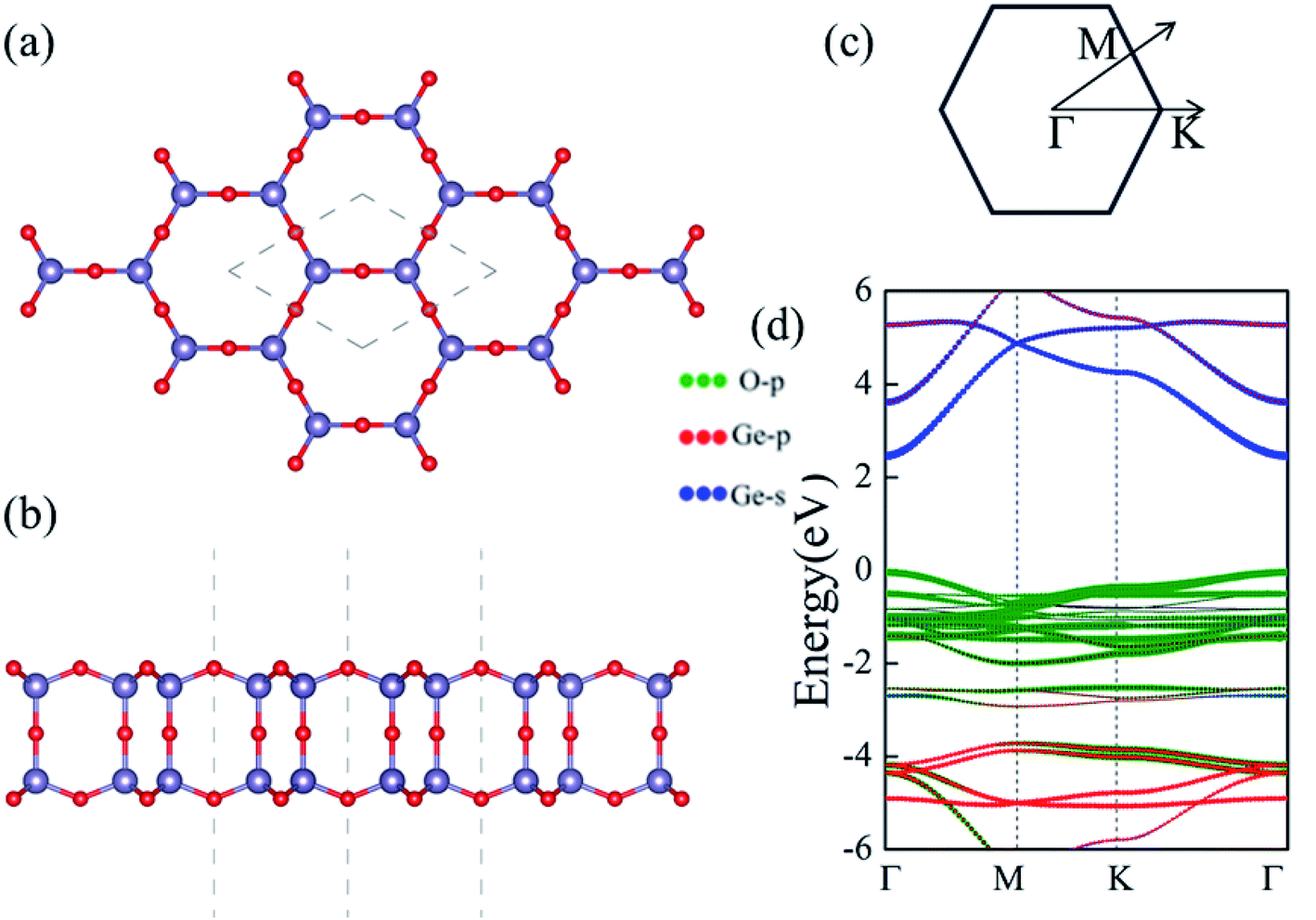 | ||
| Fig. 1 Structure schematics of α-2D-germanene dioxide monolayer in a 2 × 2 supercell from the top (a) and side (b) views; the hexagonal primitive cells are enclosed in the gray dashed line. (d) Band structure of α-2D-germanene dioxide monolayer computed at the PBE level. (c) Schematic diagram of the first Brillouin zone. | ||
Methods
In the framework of DFT,37 the Vienna Ab initio Simulation Package (VASP)37,38 was used to optimize the initial structure using the method of projector augmented wave (PAW).39 In the general gradient approximation (GGA) around the optimization process, the exchange–correlation function for selecting Perdew–Burke–Ernzerhof (PBE)40,41 was used to relax the force of atoms in the system, until the force of each atom in the system was less than 0.1 eV nm−1. The cut-off kinetic energy is set to 360 eV. At the time of calculation, the doped systems were modeled with periodic geometry, growing along the Y-axis. Respectively, the Brillouin zone (BZ) was sampled using a 9 × 9 × 1 gamma-centered Monkhorst–Pack grid, and the vacuum space was set to 30 Å to minimize artificial interactions between neighboring slabs.42 All structures were fully optimized, including cell parameters and atomic coordinates. Phonon dispersion curves were obtained using the Phonopy package.43Results and discussion
Intrinsic structural and electronic properties
We first present the geometric and electronic structures of the α-2D-germanene dioxide, as shown in Fig. 1. The α-2D-germanene dioxide has a hexagonal honeycomb structure, and the relaxed lattice parameter is found to be a = 5.75 Å. The band structure is plotted in Fig. 1d. In the top view, α-2D-germanene, like graphene, has a hexagonal crystal structure and an electronic performance like indirect-gap semiconductors. The α-2D-germanene dioxide monolayer exhibits (quasi) direct-gap semiconducting character with a PBE-Eg of 2.50 eV (see Fig. 1d). It has a larger band gap than MoS2 (bandgap = 1.9 eV), and is more easily used as short-wavelength light-emitting devices, ultraviolet detection and high-temperature, and high-power electronic devices. The valence band maximum (VBM) is based on the hybridized O 2p orbitals, while the conduction band minimum (CBM) derives from the hybridized Ge 4s orbitals.Stability
First, α-2D-germanene dioxide was considered to determine its energetic stabilities. Fig. 2 shows the formation energy with area per Ge atom for germanene dioxide (α-2D-germanene dioxide). The formation energy of the α-2D-germanene dioxide configuration with respect to its constituent atoms is calculated as:| Eform = (Etotal − NGeEGe − NOEO)/(NGe + NO) |
 | ||
| Fig. 2 (a) Variations of the free energy from 1 to 5 ps during AIMD at the temperature of 300 K. (b) Calculated formation energy vs. area/Ge atom for α-2D-germanene dioxide. (c) Phonon dispersion curves. (d) Deformation charge density (with isosurface of 0.01 e Å−3). | ||
Next, the thermal stabilities of the germanene dioxide configurations are calculated by ab initio molecular dynamics (AIMD) simulations in Fig. 2a. The MD simulations selected the supercell of 4 × 4 × 1 based on the Nośe thermostat at 500 K.45 The phonon dispersion (based on Vibra of SIESTA utility46) curves show the dynamic stability of α-2D-germanene dioxide (Fig. 2c). The deformation charge density shown in Fig. 2d suggests the charge transfer from Ge to O yielding the charge of Si to be 3.52e by Bader analysis. The same structure of the silica sheet in Russia (0001) (i.e. double silicon layer) was recently synthesized.14 This indicates that our material is likely to be prepared.
Carrier mobility
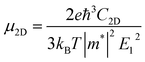
The carrier mobility (μ) of α-2D-germanene dioxide is calculated based on the deformation potential (DP)47 theory as proposed by Bardeen and Shockley, which has been proven to be reasonable in estimating μ of 2D materials. Thus, the carrier mobility (μ) of α-2D-germanene dioxide, as predicted using the DP theory, is calculated as:where e is the electron charge, ℏ is reduced Planck, kB is Boltzmann's constant and T is the temperature which set to 300 K, while m*, E1, and C2D are the effective mass, deformation potential constant, and in-plane stiffness, which will appear in the next calculation. The effective masses (m* = ℏ2(∂2E/∂K2)−1) of electrons and holes associated with the direct semiconducting α-2D-germanene dioxide are computed. Interestingly, the effective mass of electrons in the ka direction (0.05 me) is much smaller than that in the kb direction (0.07 me), indicating the easy drift of electrons in the ka direction. However, the holes entail an effective mass of ∼0.41/0.053 me (ka/kb), suggesting the easy drift of holes in the kb direction. In addition, the small effective mass in a direction could promise high carrier mobility for α-2D-germanene dioxide in this direction. By fitting the change of total energy (E) versus the uniaxial strain (ε), as shown in Fig. 3a, the in-plane stiffness C2D = [∂2E/∂δ2]/S0. S0, the area of α-2D-germanene dioxide along a and b directions, are evaluated to be 96.73 and 99.21 N m−1, respectively, as shown in Table 1. The absolute DP constant E1(= dEedge/dδ) for electrons along a and b directions is calculated to be 16.11 and 14.53 eV, respectively, as shown in Table 1. According to the calculated effective mass m*, C2D and E1, the electron mobility can be evaluated based on Table 1. Interestingly, the holes mobility in the ka direction can be as high as 4.09 × 103 cm2 V−1 s−1, which is much higher than that of MoS2 (∼3.0 cm2 V−1 s−1)48 at room temperature. Therefore, the high carrier mobility found in the study is of great significance to the study of electron transport.
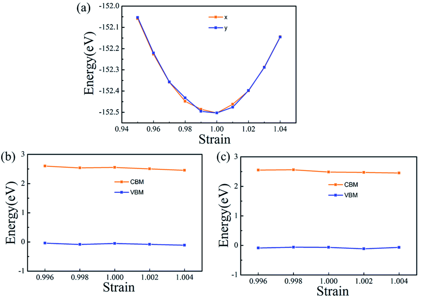 | ||
| Fig. 3 (a) Energy difference between the total energy of the monolayer under uniaxial strain and that of monolayer under no strain as a function of strain along ka and kb directions. The in-plane stiffness C2D can be obtained after fitting the parabola. The energy of VBM and CBM shift with respect to the lattice dilation and compression along x (b) and y (c) directions. The slopes of the straight lines correspond to the DP constant along different directions for electrons and holes. | ||
| Direction | Carrier type | |m*| (me) | |E1| (eV) | C2D (N m−1) | μ (cm2 (V−1 s−1)) | τ (fs) |
|---|---|---|---|---|---|---|
| ka | Holes | 0.41 | 11.08 | 96.73 | 4.09 × 10³ | 83.55 |
| Electrons | 0.05 | 16.11 | 2.12 × 10³ | 43.31 | ||
| kb | Holes | 0.05 | 11.56 | 99.21 | 3.76 × 10³ | 76.81 |
| Electrons | 0.07 | 14.53 | 1.36 × 10³ | 27.78 |
Optical properties
The optical properties are tied closely to the dielectric function which can be calculated by:| ε(ω) = ε1(ω) + iε2(ω) |
In addition, the absorption coefficient I(ω) was obtained by:
The properties of materials are also directly reflected in the optical properties. The wide bandgap of α-2D-germanene dioxide means that it can more easily be used in short-wavelength light-emitting devices and ultraviolet detection compared with MoS2. Attracted by the proper band gap and excellent electronic properties of α-2D-germanene dioxide, we further explored the light absorption of α-2D-germanene dioxide. As shown in Fig. 4b, α-2D-germanene dioxide shows absorption starting at ∼2.5 eV, with two main absorption peaks from ∼5.5 to ∼7.5 eV, corresponding to significant light absorption at the ultraviolet region of the solar spectrum. The incident light can be effectively absorbed in three directions, with the adsorption coefficients increasing up to the order of 4.5 a.u., as shown in Fig. 4a. As shown in Fig. 4b, the plot of dielectric functions versus energy shows the same trend. Therefore, α-2D-germanene dioxide seems rather attractive for efficient light harvesting and may have promising applications in optoelectronics.
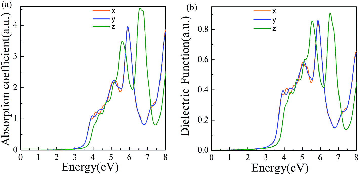 | ||
| Fig. 4 (a) Computed imaginary absorption coefficient for α-2D-germanene dioxide along different incident light directions. (b) Computed imaginary dielectric functions versus energy. | ||
Conclusions
In conclusion, based on first-principles calculations, we show that α-2D-germanene dioxide has an appropriate band gap and excellent electronic and optical properties, attracting great attention as a possible candidate for electronic devices. α-2D-germanene dioxide shows semiconductor properties, with a gap reaching up to 2.50 eV. To our delight, α-2D-germanene dioxide is fairly stable according to calculations of formation energy, MD simulation and phonon dispersion curves. α-2D-germanene dioxide possesses a very high electron mobility of 4.09 × 103 cm2 V−1 s−1 along the ka direction, which is much higher than that of MoS2 (∼3.0 cm2 V−1 s−1). Furthermore, the excellent optical properties makes α-2D-germanene dioxide an excellent optical device. Prominent stability, appropriate band gap, high carrier mobility and remarkable light absorption render the studied materials highly suitable for applications in electronics and optoelectronics.Conflicts of interest
There are no conflicts to declare.Acknowledgements
This work was supported by the National Natural Science Foundation of China (Grant Nos. 61571210, 61172028, and 11434006), and Shandong Provincial Natural Science Foundation of China (Grant No. ZR2018QA006).References
- S. Shaikhutdinov and H.-J. Freund, Ultrathin silica films on metals: the long and winding road to understanding the atomic structure, Adv. Mater., 2013, 25, 49–67 CrossRef CAS PubMed.
- T. Demuth, Y. Jeanvoine, J. Hafner and J. Angyan, Polymorphism in silica studied in the local density and generalized-gradient approximations, J. Phys.: Condens. Matter, 1999, 11, 3833 CrossRef CAS.
- X. Q. Chen, H. Y. Niu, D. Li and Y. Li, Modeling hardness of polycrystalline materials and bulk metallic glasses, Intermetallics, 2011, 9, 1275–1281 CrossRef.
- S. Stishov and N. Belov, Crystal structure of a new dense modification of silica SiO2, Dokl. Akad. Nauk SSSR, 1962, 143, 951 CAS.
- E. Chao, J. Fahey, J. Littler and D. S. Milton, SiO2, a very high pressure new mineral from Meteor Crater, Arizona, J. Geophys. Res., 1962, 67, 419–421 CrossRef CAS.
- D. M. Teter, R. J. Hemley, G. Kresse and J. Hafner, High pressure polymorphism in silica, Phys. Rev. Lett., 1998, 80, 2145 CrossRef CAS.
- S. R. Shieh, T. S. Duffy and B. Li, Strength and elasticity of SiO2 across the stishovite−CaCl2 -type structural phase boundary, Phys. Rev. Lett., 2002, 89, 255507 CrossRef PubMed.
- G. X. Wang, G. C. Loh, R. Pander and S. P. Karna, Novel Two-Dimensional Silica Monolayers with Tetrahedral and Octahedral Configurations, J. Phys. Chem. C, 2015, 119, 15654–15660 CrossRef.
- V. Prakapenka, G. Shen, L. Dubrovinsky, M. Rivers and S. Sutton, High pressure induced phase transformation of SiO2 and GeO2: difference and similarity, J. Phys. Chem. Solids, 2004, 65, 1537–1545 CrossRef CAS.
- T. K. Todorova, M. Sierka, J. Sauer, S. Kaya, J. Weissenrieder, J. Lu, H. J. Gao, S. Shaikhutdinov and H. J. Freund, Erratum: atomic structure of a thin silica film on a Mo(112) substrate: a combined experimental and theoretical study, Phys. Rev. B: Condens. Matter Mater. Phys., 2006, 73, 165414 CrossRef.
- J. Weissenrieder, S. Kaya, J.-L. Lu, H.-J. Gao, S. Shaikhutdinov, H.-J. Freund, M. Sierka, T. K. Todorova and J. Sauer, Atomic structure of a thin silica film on a Mo(112) substrate: a two-dimensional network of SiO4 tetrahedra, Phys. Rev. Lett., 2005, 95, 076103 CrossRef CAS PubMed.
- T. Schroeder, M. Adelt, B. Richter, M. Naschitzki, M. Bäumer and H.-J. Freund, Growth of well-ordered silicon dioxide films on Mo(1 1 2), Surf. Rev. Lett., 2000, 7, 7–14 CrossRef CAS.
- J. Seifert, D. Blauth and H. Winter, Evidence for 2D-Network Structure of Monolayer Silica Film on Mo(112), Phys. Rev. Lett., 2009, 103, 017601 CrossRef CAS PubMed.
- D. Löffler, J. J. Uhlrich, M. Baron, B. Yang, X. Yu, L. Lichtenstein, L. Heinke, C. Büchner, M. Heyde, S. Shaikhutdinov, H.-J. Freund, R. Włodarczyk, M. Sierka and J. Sauer, Growth and structure of crystalline silica sheet on Ru(0001), Phys. Rev. Lett., 2010, 105, 146104 CrossRef PubMed.
- M. Heyde, S. Shaikhutdinov and H.-J. Freund, Two-dimensional silica: crystalline and vitreous, Chem. Phys. Lett., 2012, 550, 1–7 CrossRef CAS.
- P. Y. Huang, S. Kurasch, A. Srivastava, V. Skakalova, J. Kotakoski, A. V. Krashenin-nikov, R. Hovden, Q. Mao, J. C. Meyer, J. Smet, D. A. Muller and U. Kaiser, Direct imaging of a two-dimensional silica glass on grapheme, Nano Lett., 2012, 12, 1081–1086 CrossRef CAS PubMed.
- A. K. Geim, I. V. Grigorieva, A. K. Geim and I. V. Grigorieva, Nature, 2013, 499, 419–425 CrossRef CAS PubMed.
- P. Miro, M. Audiffred and T. Heine, An atlas of two-dimensional materials, Chem. Soc. Rev., 2014, 43, 6537–6554 RSC.
- K. Zheng, X. Yang, H. Cui, Q. Yang, H. Ye, D. Xiong, S. Ingebrandt and X. Chen, Intriguing Electronic Insensitivity and High Carrier Mobility in Monolayer Hexagonal, J. Mater. Chem. C, 2018, 6, 4943 RSC.
- S. Guo, Z. Zhu, X. Hu, W. Zhou, X. Song, S. Zhang, K. Zhang and H. Zeng, Tailored design of functional nanoporous carbon materials toward fuel cell applications, Nanoscale, 2018, 10, 8397 RSC.
- Z. Gao, X. Dong, N. Li and J. Ren, Controllable Electrochemical Synthesis of Hierarchical ZnO Nanostructures on FTO Glass, Nano Lett., 2017, 17, 772 CrossRef CAS PubMed.
- J. Jiang, Q. Liang, R. Meng, Q. Yang, C. Tan, X. Sun and X. Chen, Exploration of new ferromagnetic, semiconducting and biocompatible Nb3X8 (X = Cl, Br or I) monolayers with considerable visible and infrared light absorption, Nanoscale, 2017, 9, 2992 RSC.
- P. Vogt, P. D. Padova, C. Quaresima, J. Avila, E. Frantzeskakis, M. C. Asensio, A. Resta, B. Ealet and G. L. Lay, Silicene: compelling experimental evidence for graphene like two-dimensional silicon, Phys. Rev. Lett., 2012, 108, 155501 CrossRef PubMed.
- A. K. Geim and K. S. Novoselov, Giant nonlocality near the dirac point in graphene, Nat. Mater., 2007, 6, 183 CrossRef CAS PubMed.
- J. Zhang, L. Wang, Q. Liu, H. Li, D. Yu, W. Mei, J. Shi, Z. Gao and J. Lu, Sub-10 nm Gate Length Graphene Transistors: Operating at Terahertz Frequencies with Current Saturation, Sci. Rep., 2013, 3, 1314 CrossRef PubMed.
- C. W. Zhang and S. S. Yan, First-principles Study of Ferromagnetism in Two-Dimensional Silicene with Hydrogenation, J. Phys. Chem. C, 2012, 116, 4163 CrossRef CAS.
- R. W. Zhang, C. W. Zhang, S. S. Li, W. X. Ji and P. J. Wang, Tunable electronic properties in the van der waals heterostructure of germanene/germanene, Phys. Chem. Chem. Phys., 2015, 17, 12194–12198 RSC.
- R. W. Zhang, C. W. Zhang, W. X. Ji and S. S. Yan, Silicane as an Inert Substrate of Silicene: A Promising Candidate for FET, J. Phys. Chem. C, 2014, 118, 25278–25283 CrossRef CAS.
- Z. Gao, X. Dong, N. Li and J. Ren, Novel Two-Dimensional Silicon Dioxide with in-plane Negative Poisson's Ratio, Nano Lett., 2017, 17, 772–777 CrossRef CAS PubMed.
- P. Vogt, P. P. De, C. Quaresima, J. Avila, E. Frantzeskakis, M. C. Asensio, A. Resta, B. Ealet and G. Le Lay, Silicene: Compelling experimental evidence for graphene like two-dimensional silicon, Phys. Rev. Lett., 2012, 108, 489–492 Search PubMed.
- L. C. L. Y. Voon, E. Sandberg, R. S. Aga and A. A. Farajian, Hydrogen compounds of group-IV nanosheets, Appl. Phys. Lett., 2010, 97, 163114 CrossRef.
- Y. M. Dou, W. X. Ji, S. F. Zhang, C. W. Zhang, P. Li and P. J. Wang, Novel 2D Germanene Dioxide Monolayers: Mechanical Properties, Hole-Mobility Values, and Carrier Mobility, Ann. Phys., 2018, 9, 1800214 CrossRef.
- Y. Wang, J. Lv, L. Zhu and Y. Ma, Crystal structure prediction via particle-swarm optimization, Phys. Rev. B: Condens. Matter Mater. Phys., 2010, 82, 094116 CrossRef.
- Y. Wang, J. Lv, L. Zhu and Y. Ma, CALYPSO: a method for crystal structure prediction, Comput. Phys. Commun., 2012, 183, 2063–2070 CrossRef CAS.
- G. Kresse and J. Furthmüller, Efficiency of ab-initio total energy calculations for metals and semiconductors using a plane-wave basis set, Comput. Mater. Sci., 1996, 6, 15–50 CrossRef CAS.
- G. Kresse and D. Joubert, From ultrasoft pseudopotentials to the projector augmented-wave method, Phys. Rev. B: Condens. Matter Mater. Phys., 1999, 59, 1758–1775 CrossRef CAS.
- M. Houssa, B. Van den Broek, E. Scalise, G. Pourtois, V. V. Afanas'ev and A. Stesmans, An electric field tunable energy band gap at silicene/(0001) ZnS interfaces, Phys. Chem. Chem. Phys., 2013, 15, 3702–3705 RSC.
- G. Kresse and J. Furthmuller, Efficient iterative schemes for ab initio total-energy calculations using a plane-wave basis set, Phys. Rev. B: Condens. Matter Mater. Phys., 1996, 54, 11169–11186 CrossRef CAS.
- G. Kresse and D. Joubert, From Ultrasoft Pseudopotential to the Projector Augmented-Wave Method, Phys. Rev. B: Condens. Matter Mater. Phys., 1999, 59, 1758–1775 CrossRef CAS.
- J. P. Perdew, A. Ruzsinszky, G. I. Csonka, O. A. Vydrov and G. E. Scuseria, Erratum: Restoring the Density-Gradient Expansion for Exchange in Solids and Surfaces, Phys. Rev. Lett., 2008, 100, 136406 CrossRef PubMed.
- J. P. Perdew, K. Burke and M. Ernzerhof, Erratum: Generalized Gradient Approximation Made Simple, Phys. Rev. Lett., 1996, 77, 3865 CrossRef CAS PubMed.
- H. J. Monkhorst and J. D. Pack, Special points for Brillouin-zone integrations, Phys. Rev. B: Solid State, 1976, 13, 5188–5192 CrossRef.
- A. Togo, F. Oba and I. Tanaka, First-principles calculations of the ferroelastic transition between rutile-type and CaCl2-type SiO2 at high pressures, Phys. Rev. B: Condens. Matter Mater. Phys., 2008, 78, 134106 CrossRef.
- Q. Li, D. Zhou, W. Zheng, Y. Ma and C. Chen, Global structural optimization of tungsten borides, Phys. Rev. Lett., 2013, 110, 136403 CrossRef PubMed.
- S. Nosé, A unified formulation of the constant temperature molecular dynamics methods, J. Chem. Phys., 1984, 81, 511 CrossRef.
- A. Postnikov, O. Pagès and J. Hugel, Lattice dynamics of the mixed semiconductors (Be, Zn) Se from first-principles calculations, Phys. Rev. B: Condens. Matter Mater. Phys., 2005, 71, 115206 CrossRef.
- A. Togo, F. Oba and I. Tanaka, First-principles calculations of the ferroelastic transition between rutile-type and CaCl2-type SiO2 at high pressures, Phys. Rev. B: Condens. Matter Mater. Phys., 2008, 78, 134106 CrossRef.
- H. Zhang, Y. Ma and Z. Chen, Quantum spin hall insulators in strain-modified arsenene, Nanoscale, 2015, 7, 19152 RSC.
| This journal is © The Royal Society of Chemistry 2019 |