
 Open Access Article
 This Open Access Article is licensed under a Creative Commons Attribution-Non Commercial 3.0 Unported Licence
Flash memory devices and bistable nonvolatile resistance switching properties based on PFO doping with ZnO
Jiahe Huanga,
Xiaofeng Zhaob,
Hongyan Zhanga,
Ju Baia,
Shuhong Wang *a,
Cheng Wang*ac,
Dongge Mad and
Yanjun Houa
*a,
Cheng Wang*ac,
Dongge Mad and
Yanjun Houa
aSchool of Chemical Engineering and Materials, Heilongjiang University, Harbin 150080, P. R. China. E-mail: openair@163.com; wangc_93@163.com
bSchool of Electronic Engineering, Heilongjiang University, Harbin 150080, P. R. China
cKey Laboratory of Functional Inorganic Material Chemistry, Heilongjiang University, Ministry of Education, Harbin 150080, P. R. China
dSchool of Materials Science and Engineering, South China University of Technology, Guangzhou 510640, P. R. China
First published on 27th March 2019
Abstract
In this study, poly(9,9-dioctylfluorene-2,7-diyl) (PFO) was synthesized through the Suzuki reaction, and it was characterized. A sandwich type memory device based on PFO and PFO:ZnO, was fabricated using rotary-coating technology. I–V characteristics of the device were studied, and the effects of ZnO nanoparticle (NP) doping content on the performances of the device were discussed. The best doping content of ZnO NPs was found by processing the experimental results (4.76 wt%). Also, the stability of the device was tested, and it was found that the device remained stable after a long testing period. Furthermore, the switching mechanism of the device was discussed.
1. Introduction
With the advancement of time, information technology has taken up a vital role in our lives, including, mobile phones, personal computers, fax machines, and media players. With the increase in the complexity of mobile devices, miniaturization and data storage become important problems. All information technologies require data storage as a support. Conventional memories are implemented on semiconductor-based integrated circuits, e.g., transistors and capacitors. Since the main driving force of memory technology and devices is the demand for mobile applications, the demand continues to grow for higher capacity, better system performance, smaller form factor and lower cost.1,2 However, physical and economic factors hinder the development of inorganic semiconductor memories. Accordingly, the development of next-generation storage devices is of huge importance.These days, organic memory devices (OMD)3 have become a rapidly developing novel electrical storage device because of its advantages of easy processing,4 low power consumption,5 high storage density6 and low cost.7 It has aroused the wide attention from scientists. In general, OMD changes the conductive state of organic thin films with external voltage, and the high conductive state and the low conductive state represent the “1” and “0” of digital storage, respectively.8
In recent years, the major field of OMD research is to employ organic/inorganic nanomaterials as substrate to fabricate devices. Since inorganic nanoparticles exhibit excellent electrical and optical properties, the doping of inorganic nanoparticles significantly improves the performance of the devices,9–12 e.g., poly(vinylidene fluoride-hexafluoropropylene) (PVDF-HFP):Ag,13 polyimide (PI):GO,14 poly(9-vinylcarbazole) (PVK):TiO2,15 polyvinylpyrrolidone (PVP):MoS2,16 and polyvinyl alcohol (PVA):CNTs.17 These studies mixed inorganic nanoparticles with organic thin films and analyzed the effects of inorganic nanoparticles with different concentrations on device performance. For instance, T. W. Kim et al.15 reported that the TiO2 weight ratio is 0.26 wt%, and the switching current ratio reaches 105. Besides, Song et al. found that the material fabricated by doping Au NPs into polyvinyl carbazole (PVK) shows a higher switch ratio, and the switch ratio reaches 105. The current switch ratio of the device is 103, and the device remains stable after multiple cycles. The electrical bistability of the device can be repeated.18 Among the numerous inorganic nanoparticles, ZnO NPs are favored by researchers because of its excellent dispersion, easy preparation and excellent electrical properties.19 It has been reported in the literature, including PVP:ZnO,20 poly(3-hexylthiophene) (P3HT):ZnO,21 and polymethylmethacrylate (PMMA):ZnO.22 After the addition of ZnO NPs, these devices exhibit better performance.
In this study, poly(9,9-dioctylfluorene-2,7-diyl) (PFO) was synthesized by Suzuki reaction. Polyfluorene refers to a typical conjugated polymer photoelectric material exhibiting excellent photoelectric properties. The storage performance of devices fabricated by pure PFO and PFO:ZnO was compared. It was found that after the addition of the ZnO NPs, the performance of polymer device was obviously improved.
2. Experimental
2.1. Material
All reagents were purchased at Sinopharm Co. Ltd, with no further purification. ZnO NPs were stored in a dry nitrogen environment, with a particle size of 10–30 nm and the specific surface area equal to or over 110 m2 g−1.2.2. Synthesis of poly(9,9-dioctylfluorene-2,7-diyl) (PFO)
The synthetic route of the polymer is presented in Scheme 1. 9,9′-Dioctyfluorene-2,7-dibornic acid bis(1,3-propanediol), ester (0.5000 g, 0.8954 mmol), 9,9-dioctyl-2,7-dibromofluorene (0.4911 g, 0.8954 mmol), Pd (PPh3)4 (0.0310 g) and methylbenzene (15 mL) were added to Schlenk in turn. Once they were dissolved, Na2CO3 solution (3 M, 15 mL) was added. The solution was stirred continuously in nitrogen atmosphere, slowly heated up to 105 °C and reacted for 48 h. When the reaction was completed, the solution was cooled to normal temperature. The organic phase was washed by distilled water. Subsequently, the organic phase was slowly dropped into methanol. By Soxhlet extraction for two days, the extractant was acetone. The final product was dried for 48 h in a vacuum and underwent characterization analysis under 1H-NMR, 13C-NMR and FT-IR spectroscopy.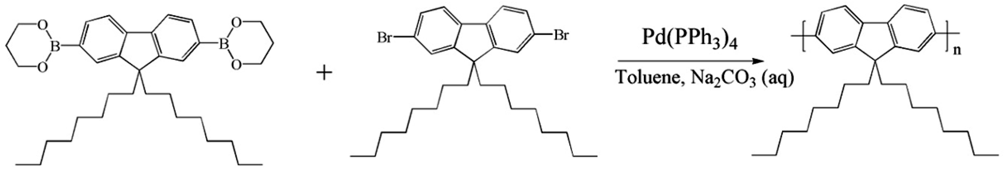 | ||
| Scheme 1 Synthetic route of PFO. | ||
2.3. Preparation of sandwich type memory device
The indium tin oxide (ITO) 2 cm × 2 cm in size was washed with detergent and deionized water, and then it underwent ultrasonic treatment for 30 min in acetone and ethanol, respectively. The finished ITO conductive glass was stored in ethanol. The synthesized polymer was dissolved in toluene with the concentration of 3 mg mL−1. The solution was sealed at normal temperature for 24 h under magnetic stirring. The solution was filtered with a polytetrafluoroethylene film (0.22 μm in diameter), and a homogeneous solution was obtained. We have surface-modified ZnO NPs before doping to make them have a certain lipophilicity. The oleic acid (1.7355 g, 6.14 mmol) was dissolved in 100 mL of absolute ethanol, ZnO NPs (0.5000 g, 6.14 mmol) were added, sonicated at 50 °C for 1 h, centrifuged and dried under vacuum.ZnO NPs were treated with chloroform as solvent and then with ultrasonic degradation for 1 h. Subsequently, the treated ZnO NPs solution was mixed with the pretreated PFO solution and continuously stirred for 1 h. Different proportions of ZnO NPs and PFO solution are listed in Table 1. ITO was covered with different concentrations of the solution by spin-coating method at the rotate speed of 1000 rpm for 20 s and then 3000 rpm for 40 s. Thereafter, the sample was covered with a copper sheet with a pore diameter of 200 μm, and the Al electrode was plated on the surface of the active layer by vacuum evaporation. The thickness of the electrode was controlled by a crystal oscillator to be about 300 nm.
| ZnO content in trichloromethane (mg mL−1) | Volume of ZnO trichloromethane solution (mL) | Volume of PFO toluene solution (3 mg mL−1) (mL) | ZnO content in the doping film (wt%) | |
|---|---|---|---|---|
| A | 0.00 | 0 | 1 | 0.00 |
| B | 0.10 | 1 | 1 | 3.23 |
| C | 0.12 | 1 | 1 | 3.85 |
| D | 0.15 | 1 | 1 | 4.76 |
| E | 0.18 | 1 | 1 | 5.66 |
| F | 0.22 | 1 | 1 | 6.83 |
3. Results and discussion
3.1. Characterization of the PFO
The yield was 72.38%. The FT-IR is shown in Fig. 1. The absorption characteristic peak at 2925 cm−1 was led to by the C–H stretching in octyl, and the tensile strength of the C![[double bond, length as m-dash]](https://www.rsc.org/images/entities/char_e001.gif) C was shown at 1457 cm−1. The absorption peak at 812 cm−1 was attributed to the tensile vibration of Ar–H.
C was shown at 1457 cm−1. The absorption peak at 812 cm−1 was attributed to the tensile vibration of Ar–H.
 | ||
| Fig. 1 The FT-IR of PFO. | ||
1H-NMR is shown in Fig. 2: 1H-NMR (400 MHz, CDCl3) δH (ppm): δ 7.82 (dd, J = 9.5, 5.6 Hz, 2H, Ha), 7.67 (d, J = 6.9 Hz, 4H, Hb, Hc), 2.07 (d, J = 37.7 Hz, 4H, Hd), 1.15 (d, J = 12.9 Hz, 24H, He, Hf, Hg, Hh, Hi, Hj), 0.80 (d, J = 7.0 Hz, 6H, Hk).
 | ||
| Fig. 2 The 1H-NMR of PFO. | ||
13C-NMR is shown in Fig. 3: 13C-NMR (100 MHz, CDCl3), δ C (ppm): 151.85 (C1), 140.55 (C6), 140.04 (C3), 126.19 (C2), 121.54 (C5), 120.00 (C4), 55.37 (C7), 40.42 (C8), 31.82 (C13), 30.06 (C10), 29.25 (C12), 23.95 (C9), 22.63 (C11), 14.08 (C14), 1.04 (C15).
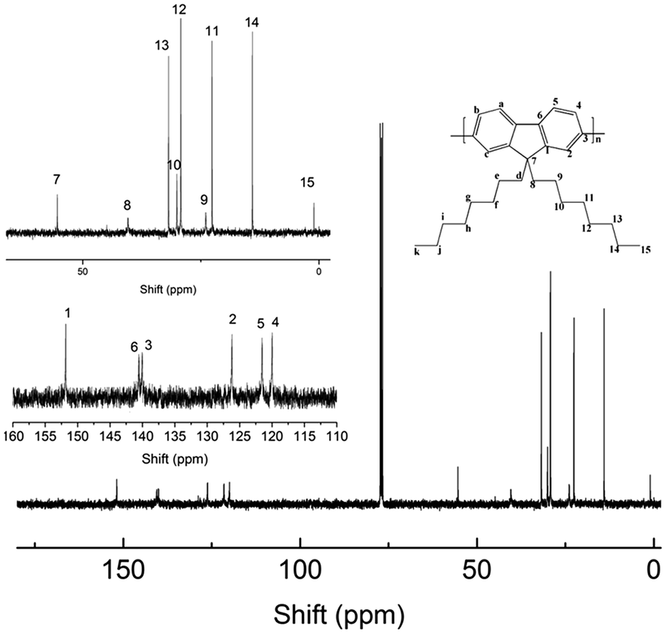 | ||
| Fig. 3 The 13C-NMR of PFO. | ||
3.2. X-ray diffraction (XRD) of ZnO NPs and microphotographs of devices
The XRD pattern of the ZnO NPs is given in Fig. 4(b). ZnO NPs with peaks correspond to (100), (002), (101), (102), (110), (103), (200), (112), (201) and (202) planes. All the peaks could be indexed to hexagonal ZnO (JCPDS. 36-1451). The transmission electron microscopy (TEM) images of ZnO NPs dispersed in the PFO toluene solution are shown in Fig. 4(c). The TEM image verifies that ZnO NPs can be better dispersed in the polymer toluene solution. Fig. 4(d) shows the cross-section scanning electron microscope (SEM) image of ITO/PFO:ZnO/Al device. This diagram suggests that the thickness of these devices is nearly 275 nm.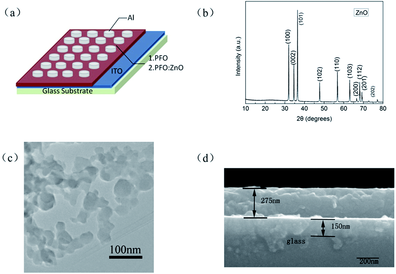 | ||
| Fig. 4 (a) Device structure; (b) XRD of ZnO NPs; (c) TEM image of ZnO NPs dispersed in the PFO toluene solution; (d) cross-section SEM image of ITO/PFO:ZnO/Al device. | ||
3.3. Characterization of the memory devices
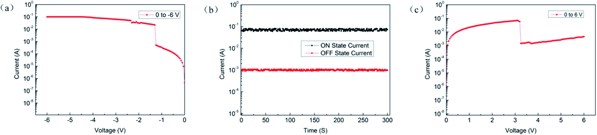
The current–voltage characteristic curve can be used to test the conductive behavior and memory performance of the polymer. To study the effects of the doping level of the mixture on the memory properties of the polymer, an independent ITO/PFO/Al sample A was tested as shown in Fig. 5(a). The 4 scanning steps constitute a current–voltage characteristic curve, the voltage changes of the 4 steps are 0 to −6 V, −6 to 0 V, 0 to 6 V and 6 to 0 V. In the first step, the current increases slowly as the voltage changes, and the current increases suddenly (3.08 × 10⁻⁵ A to 8.23 × 10⁻³ A) when the voltage reaches −1.2 V. Also, the device is switched from low conductivity state to high conductivity state. This step corresponds to the “write” course in the digital storage, and voltage of this step is named threshold voltage. At this time, the device is in the “ON” state, the ON/OFF current ratio is 267, and the low resistance state of the device is kept in the second step. The voltage change of the second step is −6 to 0 V, corresponding to the “read” process. When the voltage is up to 0 V, a reverse voltage will be applied from 0 to 6 V, which is known as step 3. When the voltage reaches 3.15 V, the device suddenly turns back to the high resistance state from the low resistance state, and this process corresponds to “erasure”. The fourth step is applied to the voltage of 6 to 0 V, in which the device displays a low electrical state (“Rereading” progress). These four steps make up a cycle of “write”–“read”–“erasure”–“reread”, indicating that it is a flash type memory device.23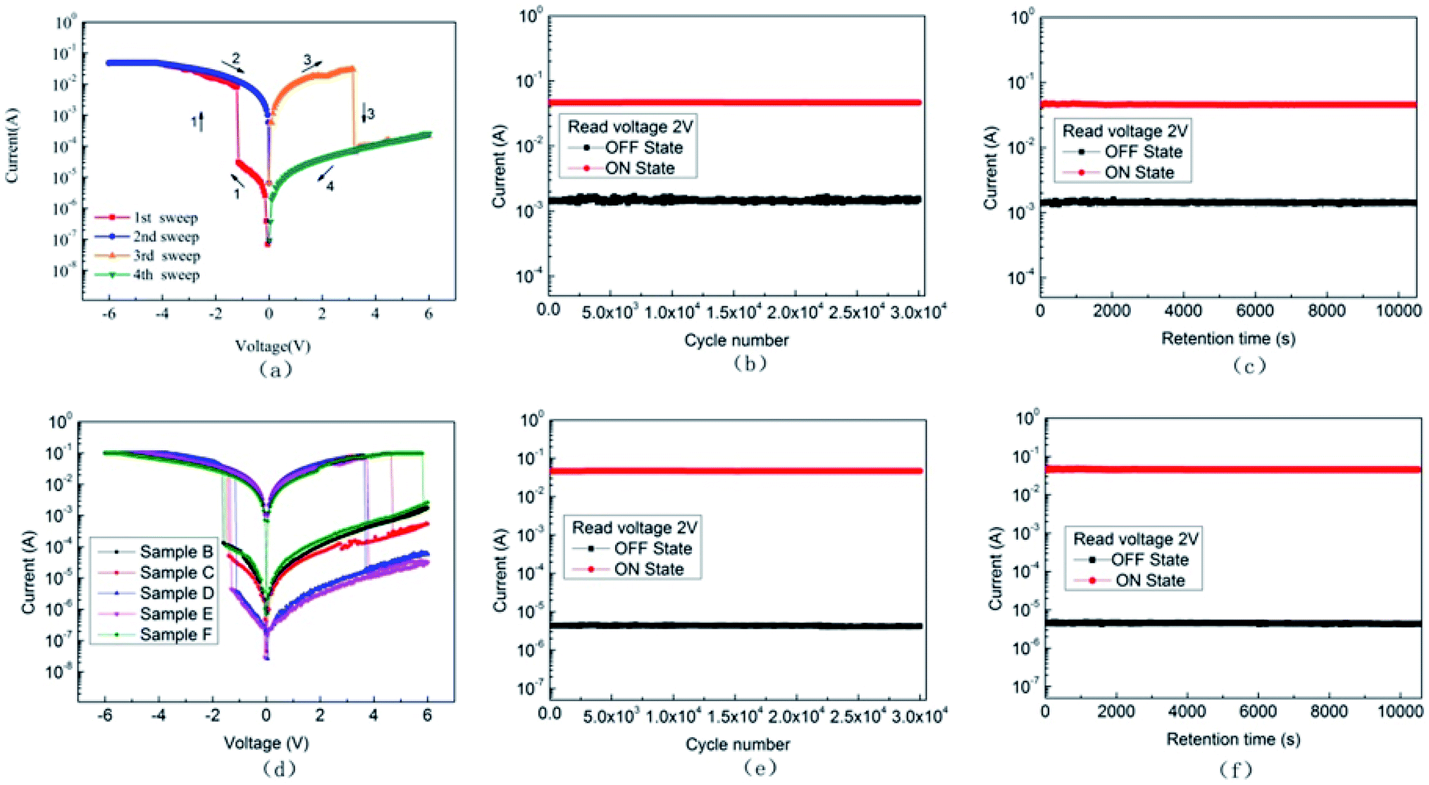 | ||
| Fig. 5 (a) I–V curves, (b) endurance performance and (c) retention performance of ITO/PFO/Al; (d) I–V curves of ITO/PFO:ZnO/Al with different ZnO NPs doping content; (e) endurance performance and (f) retention performance of sample D. | ||
The stability of memory device is a crucial parameter. Thus, to confirm its retention and persistence performance, two different tests were performed, and the test data are shown in Fig. 5(b) and (c). Fig. 5(b) shows that the current remains stable in 3 × 10⁴ cycles under a 2 V pulses (pulse period = 2 ms, pulse width = 1 ms). In Fig. 5(c), the current remained stable near the initial value for more than 3 h without attenuation, suggesting that the device has excellent stability and the ability to read multiple times.
Based on the above research on pure PFO thin film devices, researchers tried to add ZnO NPs into polymers. To clarify the effects of ZnO NPs on the performance of memory devices, PFO:ZnO mixtures with different concentrations were prepared. The current voltage curves of ITO/PFO:ZnO/Al devices doped with different proportions of ZnO NPs are shown in Fig. 5(d). Similar to the process of sample A, the threshold voltage of sample B, C, D, E, F are −1.6, −1.4, −1.1, −1.3 and −1.5 V, respectively. The ON/OFF current ratio are 3 × 10², 5 × 10², 6 × 10³, 3 × 10³ and 3 × 10², respectively. Fig. 5(e) and (f) the endurance performance and retention performance of sample D. The cycle numbers of the device were more than 3 × 10⁴, and the current did not decay for more than 3 h, showing good stability. By these tests, it was found that the memory behavior of PFO is consistent with previous reports, and both exhibited flash-type non-volatile memory features. It was also found that the polymer film doped with ZnO NPs has a higher the ON/OFF current ratio than the film reported in the literature (this study was 6000, while 500 was reported in the literature). Also, the stability is better, which can reduce the misreading rate of the file.24
In order to ensure that the device could remain the ON state, we did a segmented scan test. First, we applied a scan voltage from 0 to −6 V, and the device switches from the OFF state to the ON state, as shown in Fig. 6(a). After that, the voltage was turned off and a 3 V reverse constant voltage was applied for 5 min. We find that the current was kept at around 6.3 × 10⁻² A without significant attenuation. Next, we applied a scan voltage from 0 to 6 V, as shown in Fig. 6(c), to switch the device from the ON state to the OFF state, turn off the voltage, and then applied a constant voltage of 3 V for 5 min. The current had no obvious attenuation at around 1.02 × 10⁻³ A and the device remains OFF state. Above that, it could be inferred that the device can remain in a highly conductive state after being turned ON state until it is artificially switched to the OFF state.
 | ||
| Fig. 6 (a) Device from OFF state to ON state; (b) current of the device at constant voltage; (c) device from ON state to OFF state. | ||
In addition, we selected 30 test results of IV characteristic curve randomly, and did the processing data of each sample, and the statistical results as shown in Fig. 7(a) and (b). The standard deviation of these data was little, therefore, these results could be used as a basis for discussion. The devices with different doping concentrations exhibited different threshold voltages and switching ratios. Thus, the addition of ZnO NPs significantly affected the performance of devices. These statistics suggested that the current switch ratio increases with the increase in ZnO NPs concentration, also it shows a downward trend once reaching its peak. This was probably because the ZnO NPs dispersed on the surface of polymer films to form electron transfer paths. With the increase in doping concentration, more ZnO NPs will be formed in the effective distance, leading to more electron transfer paths. When the voltage reaches the threshold voltage, a lot of electrons will pass through the film, thereby increasing current switching ratio. At the same time, the threshold voltage is reduced gradually until a minimum occurs at the same level because the smaller the spacing of ZnO NPs, the lower the activation energy required for effective carrier transitions.25
 | ||
| Fig. 7 (a) The threshold voltage and (b) the ON/OFF current ratio of ITO/PFO:ZnO/Al devices with different concentration of ZnO NPs; (c) the ON/OFF current ratio of ITO/PFO/Al device and ITO/PFO:ZnO/Al device. | ||
However, it was found that excessive concentration of doping will decrease the ON/OFF current ratio of the device. This was because the excess of ZnO NPs will lead to a smaller distance between isolated nanoparticles, so the transport of carriers required to overcome the obstacles becomes smaller. To reduce the ON/OFF current ratio, the switching behavior will disappear when the doping concentration is further increased.26 Fig. 6(c) shows that the flash window of the device with 4.76 wt% (sample D) doping level is significantly improved compared with ITO/PFO/Al (sample A).
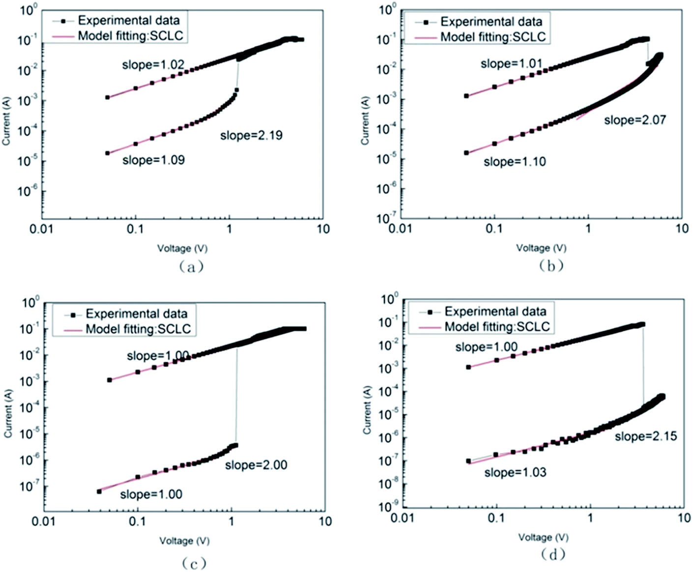
Fig. 8 shows the slope of the fitting curve of ITO/PFO/Al and ITO/PFO:ZnO/Al non-volatile memory devices exhibiting high resistance and low resistance. As shown in Fig. 8(a) and (b), the slope of fitting curves of ITO/PFO/Al devices in ON state was 1.02 and 1.01 respectively. This reflects that the conduction principle of the device is consistent with Ohm's law, and the current and voltage are linear. At the OFF state, the slope of the curve approaches to “1” at the lower voltage (1.09 and 1.10). Subsequently, a steep slope appears at high voltage (the slope is 2.19 and 2.07), and the current is proportional to the square of the voltage. This suggests that the conduction behavior is consistent with Child's law. It is therefore inferred that the switching memory behavior of ITO/PFO/Al may be guided by space charge limited current (SCLC).27
 | ||
| Fig. 8 Linear fitting and corresponding slopes for ITO/PFO/Al (a) set, (b) reset and ITO/PFO:ZnO/Al device based on sample D (c) set, (d) reset. | ||
Furthermore, the same conclusion can be drawn by the double logarithmic curve of ITO/PFO:ZnO/Al as shown in Fig. 8(c) and (d). In the ON state, the current has a linearly relation to the voltage, and the slopes are 1.00 and 1.00, respectively, also following Ohm's law. In the OFF state, the same situation appears at low voltage (slope = 1.00 and 1.03) and then at high voltage to Child's law (slope = 2.00 and 2.15). Likewise, it is inferred that the conduction behavior of ITO/PFO:ZnO/Al devices is also dominated by SCLC.
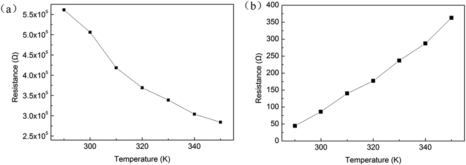
It is shown in Fig. 9 that the resistance temperature dependent of the device in HRS and LRS. It can be observed from Fig. 9(a) that the resistance of the HRS decreases with increasing temperature and it is a nonlinear relationship, which it could be inferred that it is a semiconductor characteristic rather than a metal behavior. However, the resistance of the LRS decreases as the temperature increases, and it shows a linear relationship and metallicity. This result is in accordance with the ohmic conduction with a slope of “1” in the open state fitted in Fig. 8. These results indicate that the conduction mechanisms of HRS and LRS are SCLC and ohmic properties respectively.
 | ||
| Fig. 9 (a) HRS and (b) LRS resistance temperature dependent. | ||
3.4. Stored process of the devices
The molecular orbital and energy levels of the polymer can be calculated. To investigate the electronic structure and transfer process of polymers, the HOMO and LUMO of PFO by DFT (B3LYP/6-31G) were calculated. The reaction of EHOMO refers to the ability of molecule to give electrons. The higher the HOMO level, the greater the propensity will be for molecules to provide electrons to receptors in low energy molecular orbitals. Also, the LUMO level represents the ability of the molecule to accept electrons. The lower the value of the LUMO level, the more likely it will be to accept electrons. These two together determine the way of molecular interaction, which can be represented by the energy band gap. The larger energy band gap (ΔE = ELUMO − EHOMO) reveals that the polymer has good carrier transport capability. The calculation of this study was theoretically estimated as listed in Table 2. The EHOMO, ELUMO and ΔE are −5.76 eV, −0.74 eV and 5.02 eV, respectively. The electron clouds of HOMO and LUMO are primarily distributed on the conjugated chain of fluorene, indicating that PFO itself exhibits the ability of electron donor and electron acceptor. The high energy band gap indicates that carriers can be transported along the polymer backbone.| Frontier molecular orbital | Energy level (eV) | |
|---|---|---|
| HOMO |  |
−5.76 |
| LUMO |  |
−0.74 |
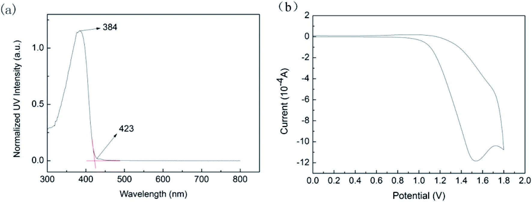
In addition, we tested the optical properties of the PFO by UV-vis. As shown in Fig. 10(a), the absorption peak of the PFO in solution was located at 423 nm. This may be due to π–π* on the PFO backbone.28 The optical band gap (Eoptg) of the PFO is 2.95 eV, which was obtained by the eqn (1).
| Eoptg = 1240/λonset | (1) |
 | ||
| Fig. 10 (a) UV-vis absorption of PFO; (b) CV curve of PFO films. | ||
The results of cyclic voltammetry (CV) as shown in Fig. 10(b). The oxidation onset potential (Eonset) is 1.53 V. Based on these data, we estimate the HOMO and LUMO energy levels of PFO. EHOMO and ELUMO were obtained by eqn (2) and (3), respectively.
| EHOMO = −(Eonset − Eox (ferrocene) + 4.80) eV, 2(Eox (ferrocene) = 0.38 V versus Ag/AgCl) | (2) |
| ELUMO = EHOMO + Eoptg | (3) |
From this, we can deduce the Eoptg, EHOMO and ELUMO were 2.93 eV, −5.95 eV and −3.02 eV, respectively. These are bias with the results of theoretical calculations, which may be due to theoretical calculations from molecular units, and the test results are derived from long chains of polymers. In addition, solvents and electrolytes may have an impact on test results. Therefore, below we use experimental data to discuss the storage process of the devices.
When the negative voltage is scanned, ITO serves as anode (−4.80 eV) and an Al as cathode (−4.27 eV).29 As shown in Fig. 11(a), the energy barrier between the cathode and the LUMO of PFO is 1.25 eV, much greater than the minimum energy barrier between the escape work of ITO and the HOMO of PFO (−5.95 eV). This suggests that it is a favorable process to inject from the metal electrode to HOMO of PFO, and the conductive course could be dominated by hole injection. After the increase in voltage, the holes move from ITO to HOMO and pass through the polymer chain. At low voltage, the initial current increases slowly as the energy barrier between Al electrode and LUMO prevents electron migration. When the voltage reaches threshold voltage, the electrons obtains energy to surmount the energy barrier will enter the films so that there is a sudden increase in current. In addition, the storage process can also be explained by the formation of conductive filaments. When a voltage is applied, a charge is injected into the active layer of the polymer. The charge trapping point in the polymer causes accumulation of charges, which it leads to redistribution of the electric field. When the voltage reaches a certain value, the charges are filled with holes, and the charges have high mobility. Afterwards, it forms the conductive filament, which can make the device switched from the OFF state to the ON state.30 These charges are conducted through the conductive filaments and keep the device in an ON state. With the progress of the voltage sweep, a reverse current occurs when a reverse voltage is applied, and considerable charges are transferred by the conductive filaments. When the voltage continues to increase, the charge will surpass the conductivity of the filament and produce Joule heat. In the meantime, excessive current will cause the charge to accumulate and electrostatic repulsion. The extra Joule heat and electrostatic repulsion generated can cause the filament to break, causing the device to return to the OFF state.31
 | ||
| Fig. 11 Energy level diagram of the (a) ITO/PFO/Al and (b) ITO/PFO:ZnO/Al device. | ||
Since the charge conduction ability of the polymer was limited, ZnO NPs could be introduced into the polymer film as the electron capture center to facilitate the injection and capture of the charge. As shown in Fig. 11(b), the work function of the surface modified ZnO NPs is generally −4.4 eV,29 a data far below the LUMO of PFO, suggesting that the Al electrode contacts ZnO NPs to form ohmic contact. It is easier to inject electrons from the cathode into the ZnO NPs than the injection of holes from the anode into the HOMO. First, electrons were injected from Al electrode to ZnO NPs and transported along the axis of ZnO NPs.24 At a certain voltage, hole injection was made, and carriers were injected to films and trapped by ZnO NPs to form a space charge layer. When the threshold voltage was reached, carriers were injected to the LUMO through the ZnO NPs axes, which suddenly increased the current. The concentration of ZnO NPs in the films affected the effective distance between adjacent ZnO NPs and promoted the charge trapping ability of the device, thereby changing the conductance behavior of the device.32 The formation of the conductive filament is similar to that above. And, by doping ZnO NPs, the carrier can be transferred along the ZnO NPs axis and also can increase the capacity of the conductive filament, which can reduce the threshold voltage of the device and increase the ON/OFF current ratio.
4. Conclusion
To sum up, conjugated polymer PFO was successfully prepared by Suzuki reaction, and it was applied in flash storage devices. Besides, devices based on PFO doping with ZnO were also assembled as active layers by spin-coating technology. Moreover, different bistable flash type electrical storage devices were developed, and the effects of different ZnO NPs content on the performance of the devices were investigated at the same time. After doping ZnO NPs, the ITO/PFO:ZnO/Al achieved excellent electrical storage performance (the best ZnO NPs content up to 4.76 wt%, sample D), the ON/OFF current ratio increased (267 to 6 × 10³), and the threshold voltage of the device was reduced (VSET from −2 to −1.1 V). In the meantime, the current is stable for more than 3 h at 2 V voltage, and the number of cycles is 3 × 10⁴ at the read pulse of 2 V. With low threshold voltage, high ON/OFF current ratio and good stability, PFO:ZnO materials exhibit a potential as a new generation of electric memristor.Conflicts of interest
The authors declare no conflict of interest.Acknowledgements
The work was financially supported by the National Natural Science Foundation of China(NSFC 51527804, 51473056, 51503058, 51573015, 61471159). Natural Science Foundation of Heilongjiang Province of China (grant number B2017010).Notes and references
- C. U. Pinnow and T. Mikolajick, J. Electrochem. Soc., 2004, 151, K13–K19 CrossRef CAS
.
- M. George, Mater. Today, 2003, 6, 38–43 Search PubMed
- C. C. Wei, J. Y. Ouyang, J. H. Tseng and Y. Yang, Adv. Mater., 2005, 17, 1440–1443 CrossRef
- J. Scott and L. Bozano, Adv. Mater., 2007, 19, 1452–1463 CrossRef CAS
- Y. Yang, J. Y. Ouyang, L. Ma, J. H. Tseng and C. C. Wei, Adv. Funct. Mater., 2006, 16, 1001–1014 CrossRef CAS
- B. Lee, H. Bae, H. Seong, D. Lee, H. Park, Y. Choi, S. Gapim, S. Kim and Y. K. Choi, ACS Nano, 2015, 9, 7306–7313 CrossRef CAS PubMed
- R. Tseng, J. Huang and Y. Yang, Nano Lett., 2005, 5, 1077–1080 CrossRef CAS PubMed
- W. Lin, S. Liu, T. Gong, Q. Zhao and W. Huang, Adv. Mater., 2014, 26, 570–606 CrossRef CAS PubMed
- G. Khurana, P. Misra and R. Katiyar, J. Appl. Phys., 2013, 114, 124508 CrossRef
- J. Shim, J. Jung, M. Lee, T. Kim, D. Son, A. Han and S. Kim, Org. Electron., 2011, 12, 1566–1570 CrossRef CAS
- B. Zhang, G. Liu, Y. Chen, L. Zeng, C. Zhu, K. Neoh, C. Wang and E. Kang, Chem.–Eur. J., 2011, 17, 13646–13652 CrossRef CAS PubMed
- C. Shih, W. Lee, Y. Chiu, H. Hsu, H. Chang, C. Liu and W. Chen, Sci. Rep., 2016, 6, 20129 CrossRef CAS PubMed
- K. Rajan, S. Bocchini, A. Chiappone, I. Roppolo, D. Perrone, K. Bejtka, C. Ricciardi, C. Pirri and A. Chiolerio, Microelectron. Eng., 2017, 168, 29 CrossRef
- J. Y. Choi, H. C. Yu, J. Lee, J. Jeon, J. Im, J. Jang, S. W. Jin, K. K. Kim, S. Cho and C. M. Chung, Polymers, 2018, 10, 901 CrossRef
- B. Cho, T. Kim, M. Choe, G. Wang, S. Song and T. Lee, Org. Electron., 2009, 10, 474 Search PubMed
- J. Liu, Z. Zeng, X. Cao, G. Lu, L. Wang, Q. Fan, W. Huang and H. Zhang, Small, 2012, 8, 3517–3522 CrossRef CAS PubMed
- S. Kishore and A. Pandurangan, RSC Adv., 2014, 4, 9905 RSC
- Y. Song, Q. Ling, S. Lim, E. Teo, Y. Tan, L. Li, E. Kang, D. Chan and C. Zhu, IEEE Electron Device Lett., 2007, 28, 107–110 CAS
- T. Dao, T. Tran, K. Higashimine, H. Okada, D. Mott, S. Maenosono and H. Murata, Appl. Phys. Lett., 2011, 99, 233303 CrossRef
- C. Lin, T. Pan, M. Chen, Y. Yang, Y. Tai and Y. Chen, Appl. Phys. Lett., 2011, 99, 023303 CrossRef
- F. Verbakel, S. C. Meskers and R. A. Janssen, J. Appl. Phys., 2007, 102, 083701 CrossRef
- D. Ick Son, C. You, W. T. Kim, J. Jung and W. Tae, Appl. Phys. Lett., 2009, 94, 132103 CrossRef
- G. Liu, X. Zhuang, Y. Chen, B. Zhang and J. Zhu, Appl. Phys. Lett., 2009, 95, 253301 CrossRef
- L. Seunghoon, O. Seunghwan, J. Yongsung, K. Juhwan, K. Rira and K. Dongyoon, Org. Electron., 2014, 15, 1290–1298 CrossRef
- G. Liu, Q. Ling, C. Zhu, S. Chan, K. Neoh and E. Kang, ACS Nano, 2009, 3, 1929–1937 CrossRef CAS PubMed
- X. Huang, B. Zheng, Z. Liu, C. Tan, J. Liu, B. Chen, H. Li, J. Chen, X. Zhang, Z. Fan, W. Zhang, Z. Guo, F. Huo, Y. Yang, L. H. Xie, W. Huang and H. Zhang, ACS Nano, 2014, 8, 8695–8701 CrossRef CAS PubMed
- Q. D. Ling, Y. Song, S. L. Lim, Y. P. Tan, C. Zhu, D. Chan, D. Kwong, E.-T. Kang and K. G. A. Neoh, Angew. Chem., Int. Ed., 2006, 118, 3013–3017 CrossRef
- C. N Chuang, C. Y. Chang, C. L. Chang, Y. X. Wang, Y. S. Lin and M. K. Leung, Eur. Polym. J., 2014, 56, 33–44 CrossRef
- D. C. Guo, Z. Y. Sun, S. H. Wang, X. D. Bai, L. D. Xu, Q. Yang, Y. Xin, R. R. Zheng, D. G. Ma, X. F. Zhao and C. Wang, RSC Adv., 2017, 7, 10323–10332 RSC
- B. Hu, F. Zhuge, X. Zhu, S. Peng, X. Chen, L. Pan, Q. Yan and R. W. Li, J. Mater. Chem., 2012, 22, 520 RSC
- Y. J. Lee, J. Wang, S. Cheng and W. Julia, ACS Appl. Mater. Interfaces, 2013, 5, 9128–9133 CrossRef CAS PubMed
- W. Zhang, C. Wang, G. Liu, X. Zhu, X. X. Chen, L. Pan, H. W. Tan, W. H. Xue, Z. H. Ji, J. Wang, Y. Chen and R. W. Li, Chem. Commun., 2014, 50, 11856–11858 RSC
| This journal is © The Royal Society of Chemistry 2019 |