
 Open Access Article
 This Open Access Article is licensed under a Creative Commons Attribution-Non Commercial 3.0 Unported Licence
The charge regulation of electronic structure and optical properties of graphitic carbon nitride under strain†
Hengshuai Li *abc,
Haiquan Huc,
Chenglin Baic,
Chunjiang Baob,
Feng Guoc,
Zhenbao Fengc and
Yongjun Liu*a
*abc,
Haiquan Huc,
Chenglin Baic,
Chunjiang Baob,
Feng Guoc,
Zhenbao Fengc and
Yongjun Liu*a
aSchool of Chemistry and Chemical Engineering, Shandong University, Jinan 250100, China. E-mail: yongjunliu_1@sdu.edu.cn
bSchool of Mechanical & Automotive Engineering, Liaocheng University, Liaocheng, 252000, China. E-mail: lihengshuai@lcu.edu.cn; Tel: +86-13475895656
cShandong Key Laboratory of Optical Communication Science and Technology, School of Physics Science and Information Technology, Liaocheng University, Liaocheng, 252000, China
First published on 6th March 2019
Abstract
The electronic structure of the graphitic carbon nitride (g-C6N6) under strain was obtained using the hybrid density functional HSE06 with a larger computational workload. The g-C6N6 could withstand 12% of the applied tensile strain. The electronic structure of g-C6N6 could be changed effectively under the tensile force. The band gap changed from direct to indirect under the strain and could be tuned in the range of 3.16 eV to 3.75 eV. At approximately 4% of the applied strain, there was a transition of the valence band maximum (VBM). A wider range of light absorption could be obtained under the strain. Our results provide a prospect for the future applications of two-dimensional materials in electronic and optoelectronic devices.
1. Introduction
In 2004, the team of Geim obtained a typical two-dimensional material, graphene.1 Since then, two-dimensional materials have attracted wide attention for their unique structures and superior properties.2–11 Exploring the properties of two-dimensional materials and regulating their properties have increasingly become an important research topics.Cao et al. synthesized a graphitic carbon nitride (g-C6N6) through the reaction of cyanuric chloride (C3N3Cl3) with sodium using NiCl2 as a catalyst.12,13 The material presented an ideal bandgap and faster carrier moving speed, indicating its potential for application in electronics and optoelectronic devices.
In order to realize its application in electronic and optoelectronic devices, it is necessary to regulate its electronic structure reasonably. It is known that application of a strain is a very effective way to adjust the electronic structure of two-dimensional materials.14,15 Two-dimensional materials can withstand greater strain than bulk materials. In previous studies, it has been proven that many two-dimensional materials present good mechanical strain properties, for example graphene, MoS2, and phosphorene.16–22 As a result, strain has become a common way to regulate the properties of two-dimensional materials effectively.23–28
In this study, the strain force was applied to g-C6N6, and the changes of its electronic structure and optical properties were analysed. To obtain more accurate results, the calculations were based on the hybrid density functional theory (HSE06).29,30 It was found that g-C6N6 could sustain of up to 12% of the applied strain. In the range of tolerable strain, with the increasing in tensile force, the band gap of energy band increased gradually. Moreover, a wider range of light absorption could be obtained under strain.
2. Method and computational details
Our first-principles calculations were performed within the framework of density-functional theory (DFT), which is implemented in the Vienna ab initio simulation package known as VASP.31–33 The electron–electron interactions were treated using a generalized gradient approximation (GGA) in the form of Perdew–Burke–Ernzerhof (PBE) for the exchange–correlation functional.34 The energy cut-off employed for the plane-wave expansion of the electron wavefunctions was set to 600 eV. The electron–ion interactions were described by the projector-augmented-wave (PAW) potentials.35,36 Four electrons for carbon (2s22p2) and five electrons for nitrogen (2s22p3) were treated as valence electrons. The supercells were repeated periodically on the x–y plane, while a vacuum region of 15 Å was applied along the z-direction to avoid mirror interactions between neighboring images. The BZ integration was sampled on a grid of 7 × 7 × 1 k-points. Structural optimizations were performed using a conjugate gradient (CG) method until the remaining force on each atom was less than 0.001 eV Å−1. A more accurate Heyd–Scuseria–Ernzerhof (HSE) screened potential method was used to calculate the band gap.29,30 Using the Kramers–Kronig dispersion relation,37 optical absorption spectra of the 2D-CTFs were computed from the imaginary part of the dielectric function.3. Results and discussion
The structure of the as-synthesized g-C6N6 is shown in Fig. 1(a). The lattice constant of the primitive cell is 7.127 Å, and the lengths of the C–C and C–N bonds are 1.510 Å and 1.341 Å, respectively. Unlike many carbon nitrides, the s-triazines ing-C6N6 is linked by C–C bonds and not by C–N bond. It has a hexagonal symmetrical planar honeycomb structure, and the chemical composition of its primitive cell is C6N6. The length of C–N bond of the g-C6N6 is 1.340 Å, which is longer than that of g-C3N4 (1.327 Å). The angle of C–N–C bond is 114.4°, and the length of C–C bond between two linked s-triazines is 1.509 Å. | ||
| Fig. 1 (a) The atomic structure diagram of g-C6N6, where the read area represents unit cell. (b) Strain–stress relation for g-C6N6. | ||
In general, the application of a strain has been regarded as an effective mechanism for regulating semiconductor performance. For two-dimensional materials this effect is more obvious because two-dimensional materials can withstand greater strain. Thus, the use of tensile strain is an effective method to adjust the properties of these materials. Next, we applied the strain to the g-C6N6 to observe the change of its properties. Tensile strain is defined as
 | (1) |
First, in order to measure the maximum borne strain force of g-C6N6, we applied biaxial strain force to the material and calculated the strain–stress relationship.38,39 As shown in Fig. 1(b), it is observed that g-C6N6 exhibits a linear elastic response when the strain is less than 7%, and a smooth curve change when the strain ranges from 7% to 12%. The maximum biaxial strain is 12%. Due to the existence of some defects,3,18,40 the tensile force of g-C6N6 is smaller than that of graphene. However, it is much larger than that of most three-dimensional materials.
In order to analyze the variation of system energy during tensile strain process, the relationship between energy and tensile strain was obtained, as shown in Fig. 2(a). With the increase in strain, the energy of the system increases gradually. When the tensile strain is less than 12%, the process of change is uniform, indicating that it is still a stable structure. The results obtained from this experiment are consistent with those obtained in Fig. 1(b).
 | ||
| Fig. 2 (a) The energy of g-C6N6 under strain. (b) The variation of two bond-lengths under strain. | ||
The variation of bond length of C–C and C–N bonds under tensile strain was obtained (Fig. 2(b)). It was found that the C–C bond length varied greatly. The extension of g-C6N6 was mainly attributed to the stretching of C–C bond; since, the bonding properties of C–C bond and C–N bond are different, the reaction to tensile strain is different, which led to the change in band structure after stretching.
Next, we studied the variation in energy band with tensile force. The band with no tensile force applied is shown in Fig. 3(a). It can be seen that there is a direct band gap of about 3.16 eV near K point using the HSE06 functional, which is consistent with previous results.41 The band gap calculated by PBE functional is 1.53 eV, which is very different from the HSE06 value and the experimental value.12,13,41 Obviously, the band gap using PBE functional is underestimated. Moreover, this band gap, using the HSE hybrid functional, is slightly different from the results obtained by the experiment. The reasons include, but are not limited to the following: experimental error, measurement error, exciton effect, and impurity defect.
 | ||
| Fig. 3 Band structures of g-C6N6 with strains (a) ε = 0%, (b) ε = 4%, (c) ε = 8%, and (d) ε = 12%. | ||
Fig. 3(b), (c) and (d) show the band structures of the materials at tensile strains ε = 4%, 8% and 12%, respectively. The energy band under the Fermi surface increases gradually at point Γ and decreases at point K, which leads to the shift of the valence band maximum (VBM) from point K to point Γ. At approximately ε = 4%, VBM is also located at two points in this band, which is a transition. After the transition, VBM remains at the Γ point of the band. It is found that the material changes from a direct band gap semiconductor to an indirect band gap semiconductor, and the band gap increases gradually. With the increase of tensile strain, the shape of the conduction band is almost unchanged; however, its position is slightly upward. From Fig. 4, the band gap of g-C6N6 increases equably from 3.16 eV to 3.75 eV, indicating that tensile force can effectively change the size of the band gap.42
 | ||
| Fig. 4 Band gap of monolayer g-C6N6 as a function of strain. | ||
To further understand the variation of the band below Fermi surface, we drew the charge–density diagram of the 27th band at Γ and K points, as is shown in Fig. 5. It can be seen that the electron cloud at K point is mainly composed of electrons around N atom, while the electron cloud at Γ point is composed of electrons around N and C atoms. That is to say, the transition probability of the electrons around N atom is high before stretching; however, the transition probabilities of the electrons around N atom and C atom are all high after stretching.43 This is also the reason why the direct band gap semiconductor changes to the indirect band gap semiconductor.
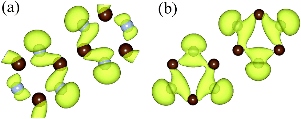 | ||
| Fig. 5 The charge density of the 27th energy band under Fermi level at point Γ (a) and at point K (b). The isosurface value is set to 0.003 Å−3. | ||
Next, we analyzed the effect of strain on optical properties. To obtain the optical absorption properties of g-C6N6, frequency-dependent dielectric matrix was calculated using HSE06 function.44 The complex dielectric constants were given as
| ε(ω) = ε1(ω) + iε2(ω) | (2) |
The absorption coefficient I(ω) was defined as45
 | (3) |
The absorption coefficient was above zero, when only if the imaginary part
| ε2(ω) > 0 | (4) |
The imaginary part was determined by a summation over empty states using the equation19
 | (5) |
 is the cell periodic part of the orbitals at the K point. A large number of empty conduction band states, which is almost twice higher than the number of valence band, were included for the summation of eqn (5).
The imaginary part of the dielectric function for the g-C6N6 was calculated using HSE06 hybrid function. The Fig. 6 shows the absorption spectra of the g-C6N6 with strains ε = 0%, ε = 4%, ε = 8%, and ε = 12%. As the tension increased, the range of the light absorption changed from 260 nm to 220 nm, where 220 nm is the down limit. When the strain reached 12%, the number of absorption peaks is clearly higher than for that without tensile strain. This results show that the tensile strain effectively changes the optical absorption property of the material, which is consistent with many previous studies.46–50 The change of optical absorption properties by tensile strain will be useful in the application of two-dimensional materials in optoelectronic devices.
 | ||
| Fig. 6 The absorption spectra of the g-C6N6 with strains ε = 0%, ε = 4%, ε = 8%, and ε = 12%. | ||
4. Conclusions
All the results in this study were obtained using the hybrid density functional HSE06 with a larger computational workload. The g-C6N6 could withstand 12% of the applied tensile strain. The electronic structure and optical absorption properties of g-C6N6 could be changed effectively by the tensile force. The band gap changed from direct band gap to indirect band gap under strain, which could be tuned in the range of 3.16 eV to 3.75 eV. At almost ε = 4%, there was a transition of VBM. A wider range of light absorption could be obtained under strain. Our results provide a prospect for the future applications of two-dimensional materials in electronic and optoelectronic devices.Conflicts of interest
There are no conflicts to declare.Acknowledgements
This study was supported by the National Natural Science Foundation of China (No. 11504153, 11504386), Science and Technology Planning Project of Higher School in Shandong Province (No. J18KA243) and Liaocheng University High-level Talents & PhD Research Start-up Foundation (No. 318051619).References
- K. S. Novoselov, A. K. Geim, S. V. Morozov, D. Jiang, Y. Zhang, S. V. Dubonos, I. V. Grigorieva and A. A. Firsov, Science, 2004, 306, 666–669 CrossRef CAS PubMed
.
- J. S. Bunch, A. M. Van Der Zande, S. S. Verbridge, I. W. Frank, D. M. Tanenbaum, J. M. Parpia, H. G. Craighead and P. L. McEuen, Science, 2007, 315, 490–493 CrossRef CAS PubMed
- C. Lee, X. Wei, J. W. Kysar and J. Hone, Science, 2008, 321, 385–388 CrossRef CAS PubMed
- J. C. Meyer, A. K. Geim, M. I. Katsnelson, K. S. Novoselov, T. J. Booth and S. Roth, Nature, 2007, 446, 60 CrossRef CAS PubMed
- K. S. Novoselov, Nature, 2005, 438, 197 CrossRef CAS PubMed
- A. Geim, Nat. Mater., 2007, 6, 183 CrossRef CAS PubMed
- H. Li, H. Hu, C. Bao, X. Zhang, A. Wang, H. Zhou and M. Zhao, Phys. B, 2014, 441, 28–32 CrossRef CAS
- M. Xu, T. Liang, M. Shi and H. Chen, Chem. Rev., 2013, 113, 3766–3798 CrossRef CAS PubMed
- H. Li, H. Hu, C. Bao, Z. Feng, F. Guo, G. Tian and Y. Liu, Diamond Relat. Mater., 2018, 87, 50–55 CrossRef CAS
- S. Guan, Y. Cheng, C. Liu, J. Han, Y. Lu, S. A. Yang and Y. Yao, Appl. Phys. Lett., 2015, 107, 231904 CrossRef
- H. Li, H. Hu, C. Bai, C. Bao, Z. Feng and F. Guo, Phys. B, 2019, 555, 91–95 CrossRef CAS
- C. Cao, F. Huang, C. Cao, J. Li and H. Zhu, Chem. Mater., 2004, 16, 5213–5215 CrossRef CAS
- J. Li, C. Cao, J. Hao, H. Qiu, Y. Xu and H. Zhu, Diamond Relat. Mater., 2006, 15, 1593–1600 CrossRef CAS
- H. Li, H. Hu, C. Bao, J. Hua, H. Zhou, X. Liu, X. Liu and M. Zhao, Phys. Chem. Chem. Phys., 2015, 17, 6028–6035 RSC
- Q.-F. Deng, L. Liu, X.-Z. Lin, G. Du, Y. Liu and Z.-Y. Yuan, Chem. Eng. J., 2012, 203, 63–70 CrossRef CAS
- G. Brunetto, P. Autreto, L. Machado, B. Santos, R. P. Dos Santos and D. S. Galvao, J. Phys. Chem. C, 2012, 116, 12810–12813 CrossRef CAS
- E. Perim, R. Paupitz, P. Autreto and D. Galvao, J. Phys. Chem. C, 2014, 118, 23670–23674 CrossRef CAS
- K. S. Kim, Y. Zhao, H. Jang, S. Y. Lee, J. M. Kim, K. S. Kim, J.-H. Ahn, P. Kim, J.-Y. Choi and B. H. Hong, Nature, 2009, 457, 706 CrossRef CAS PubMed
- H. Li, H. Hu, C. Bao, F. Guo, X. Zhang, X. Liu, J. Hua, J. Tan, A. Wang and H. Zhou, Sci. Rep., 2016, 6, 29327 CrossRef CAS PubMed
- A. Castellanos-Gomez, M. Poot, G. A. Steele, H. S. Van der Zant, N. Agraït and G. Rubio-Bollinger, Nanoscale Res. Lett., 2012, 7, 233 CrossRef PubMed
- S. Bertolazzi, J. Brivio and A. Kis, ACS Nano, 2011, 5, 9703–9709 CrossRef CAS PubMed
- X. Peng, Q. Wei and A. Copple, Phys. Rev. B: Condens. Matter Mater. Phys., 2014, 90, 085402 CrossRef
- N. Levy, S. Burke, K. Meaker, M. Panlasigui, A. Zettl, F. Guinea, A. C. Neto and M. Crommie, Science, 2010, 329, 544–547 CrossRef CAS PubMed
- F. Guinea, M. Katsnelson and A. Geim, Nat. Phys., 2010, 6, 30 Search PubMed
- J. Feng, X. Qian, C.-W. Huang and J. Li, Nat. Photonics, 2012, 6, 866 CrossRef CAS
- Q. Zhang, Y. Cheng, L.-Y. Gan and U. Schwingenschlögl, Phys. Rev. B: Condens. Matter Mater. Phys., 2013, 88, 245447 CrossRef
- A. Rodin, A. Carvalho and A. C. Neto, Phys. Rev. B: Condens. Matter Mater. Phys., 2014, 112, 176801 CAS
- R. Fei and L. Yang, Nano Lett., 2014, 14, 2884–2889 CrossRef CAS PubMed
- J. Heyd, G. E. Scuseria and M. Ernzerhof, J. Chem. Phys., 2003, 118, 8207–8215 CrossRef CAS
- J. Heyd, G. E. Scuseria and M. Ernzerhof, J. Chem. Phys., 2006, 124, 219906 CrossRef
- G. Kresse, Phys. Rev. B: Condens. Matter Mater. Phys., 1993, 47, 558 CrossRef CAS
- G. Kresse and J. Hafner, Phys. Rev. B: Condens. Matter Mater. Phys., 1994, 49, 14251 CrossRef CAS
- G. Kresse, Phys. Rev. B: Condens. Matter Mater. Phys., 1996, 54, 11169 CrossRef CAS
- J. P. Perdew, Phys. Rev. Lett., 1996, 77, 3865 CrossRef CAS PubMed
- P. Blöchl, Phys. Rev. B: Condens. Matter Mater. Phys., 1994, 50, 17953 CrossRef
- G. Kresse, Phys. Rev. B: Condens. Matter Mater. Phys., 1999, 59, 1758 CAS
- M. Gajdoš, K. Hummer, G. Kresse, J. Furthmüller and F. Bechstedt, Phys. Rev. B: Condens. Matter Mater. Phys., 2006, 73, 045112 Search PubMed
- D. Roundy and M. L. Cohen, Phys. Rev. B: Condens. Matter Mater. Phys., 2001, 64, 212103 CrossRef
- W. Luo, D. Roundy, M. L. Cohen and J. Morris Jr, Phys. Rev. B: Condens. Matter Mater. Phys., 2002, 66, 094110 Search PubMed
- J. Wu, B. Wang, Y. Wei, R. Yang and M. Dresselhaus, Mater. Res. Lett., 2013, 1, 200–206 CrossRef CAS
- K. Srinivasu, B. Modak and S. K. Ghosh, J. Phys. Chem. C, 2014, 118, 26479–26484 CAS
- X. Xue, Y. Feng, L. Liao, Q. Chen, D. Wang, L. Tang and K. Chen, J. Phys.: Condens. Matter, 2018, 30, 125001 CrossRef PubMed
- F. Ning, D. Wang, L. Tang, Y. Zhang and K. Chen, J. Appl. Phys., 2014, 116, 094308 CrossRef
- F. Ning, D. Wang, Y. Feng, L. Tang, Y. Zhang and K. Chen, J. Mater. Chem. C, 2017, 5, 9429–9438 RSC
- H. Zhang, D. Wu, Q. Tang, L. Liu and Z. Zhou, J. Mater. Chem. A, 2013, 1, 2231–2237 RSC
- R. R. Nair, P. Blake, A. N. Grigorenko, K. S. Novoselov, T. J. Booth, T. Stauber, N. M. Peres and A. K. Geim, Science, 2008, 320, 1308 CAS
- K. Mak and C. Lee, Phys. Rev. Lett., 2010, 105, 136805 CrossRef PubMed
- Q. H. Wang, K. Kalantar-Zadeh, A. Kis, J. N. Coleman and M. S. Strano, Nat. Nanotechnol., 2012, 7, 699 CAS
- Q. Li, L. Tang, C. Zhang, D. Wang, Q. Chen, Y. Feng, L. Tang and K. Chen, Appl. Phys. Lett., 2017, 111, 171602 CrossRef
- L. Tang, L. Tang, H. Geng, Y. Yi, Z. Wei, K. Chen and H. Deng, Appl. Phys. Lett., 2018, 112, 012101 CrossRef
Footnote |
| † Electronic supplementary information (ESI) available. See DOI: 10.1039/c9ra00396g |
| This journal is © The Royal Society of Chemistry 2019 |