
 Open Access Article
 This Open Access Article is licensed under a Creative Commons Attribution-Non Commercial 3.0 Unported Licence
Bioinspired transfer method for the patterning of multiple nanomaterials
Xuan Wanga,
Bingbing Gao *b and
Zhongze Gu*c
*b and
Zhongze Gu*c
aCollege of Safety Science and Engineering, Nanjing Tech University, Nanjing, 210009, China
bSchool of Pharmaceutical Sciences and School of Biotechnology and Pharmaceutical Engineering, Nanjing Tech University, Nanjing 211816, China. E-mail: kobin1989@foxmail.com
cState Key Laboratory of Bioelectronics, School of Biological Science and Medical Engineering, Southeast University, Nanjing, 210096, China. E-mail: gu@seu.edu.cn
First published on 4th February 2019
Abstract
Patterned nanomaterials have promising applications in various fields, particularly for microfluidic analysis and functional surfaces. Studies on such materials have focused on developing effective methods for fabricating patterns with various nanomaterials. Here, inspired by pollen transfer by bees, we present a simple and effective method for patterning multiple functional materials onto flexible substrates by using adhesive tapes. With the advantages of high alignment accuracy, high pattern resolution and not requiring additional etching or harsh processes, the proposed method can easily be applied to diverse nanomaterials that would not be tolerant of physical, thermal, or chemical treatments, as such treatments could deform the thin film and alter its functionalities. Patterned devices were fabricated and showed excellent performance, demonstrating the applicability of this simple and practical transfer printing technique. The proposed patterning method possesses the distinct advantages of a short operating time and high patterning yield, which highlight the considerable potential for the application of this method for optical and biomedical devices.
1 Introduction
Recently, the patterning of functional structures has attracted much attention from the scientific community and is being exploited in a wide range of applications, such as nanophotonics, point-of-care testing, environmental monitoring, biosensors, and energy storage.1–7 Several methods, including plasma etching, direct laser writing, photolithography, and focused ion beam patterning, have been reported for preparing patterns on the surfaces of supporting substrates.8–11 However, these methods suffer from various limitations, e.g., high cost, insufficient resolution, requiring sophisticated instruments, and complex or inconvenient patterning processing steps, hindering their practicality and applicability. Hence, facile, effective and low-cost patterning methodologies are attractive. The current trend is to pattern using specialized, commercially available printers. These printers offer good resolution and allow fast prototyping.As one of the most promising fabrication techniques, transfer printing can be used for the development of optical and biomedical devices because it enables the formation of functional materials on a wide range of substrates, such as plastics and planar surfaces.12,13 Typically, transfer printing involves three main steps: (1) preparation of the film on a donor substrate, (2) transfer of the film from the donor substrate to a stamp, and (3) transfer of the film on the stamp to a receiving substrate.14 The conventional transfer printing method requires a complicated and high-cost etching process, which frequently damages the material. Therefore, a new transfer method that is simple, nondestructive and compatible with printing techniques is required.
In nature, touching-sensing/transferring is the most basic but also the most important way that organisms interact with the world; by simply touching objects, organisms gain information or essential nutrients from the outside word. Among such interactions, insect pollination via the touching and transferring system offers nutrients for the insects and helps plants reproduce. Insect pollination is a key ecosystem service that is critical for the fruit set of many crop species.15 Up to 75% of the crops used for human food require insect pollination.16 As selective and efficient pollinators, bees facilitate food production and plant breeding by enabling or improving fruit and seed set. During flower visitation, bees always carry some amount of pollen on their bodies to facilitate pollen transfer. When they fly away, they can transfer the pollen on their bodies to other flowers. Thus, inspired by pollen transfer by bees, we present a facile method of transfer different materials to produce inexpensive and precise patterns by combining common printing with transfer printing. As a soft contact method, this system is well suited for the generation of patterns. Patterns based on transfer printing could allow convenient and low-cost fabrication while avoiding harsh fabrication conditions, additional etching processes, complex operations and drastic temperature changes. Thus, this method can simplify the process of obtaining patterned functional structures on flexible substrates. Moreover, transfer printing can be widely used with different materials to generate different patterning devices.
Commercial adhesive tape has been widely applied in a variety of methods for fabricating microstructured device due to its fine adhesion ability and flexibility. Therefore, in this study, tapes were chosen as substrates for the fabrication of patterns because of their ease of use, low cost and broad availability. Cellulose, Morpho menelaus (M. menelaus) wings, photonic crystals (PhCs) and graphenes are selected as model materials. Cellulose is naturally abundant, environmentally benign, renewable, and biodegradable, and its biocompatibility allows it to serve as a surface for biological reagents without hindering their activity.17–19 The M. menelaus butterfly is famous for its iridescent wing scales, and it has gradually found multiple functions. Due to its unique structural and optical properties, various technologies, e.g., in infrared sensors, gas sensors, and surface-enhanced Raman spectroscopy substrates, have been inspired by M. menelaus wings.20–22 PhCs are highly ordered materials that have been used in many different research fields due to their unique optical properties and structures.23–27 Hence, there is great interest in patterning structures for use in PhCs materials. Graphenes have attracted widespread attention owing to their fascinating physical properties, such as high electrical conductivity, ultrahigh mobility, and high elasticity.28–30 With its high conductivity, patterned graphene could be utilized as a conductive pad or connector for graphene-based electronic devices.31
Herein, we report a simple and effective approach for patterning different materials with feature with controllable sizes and shapes on tapes using transfer printing. Material-coated glass substrates were contacted with a patterned tape. The patterned tape can easily be fabricated by printing, which may enable cost-effective production. The tape is then contacted with the material. As the binding energy of the Si/SiO2 substrate for the material is weaker than that of tape, the material can easily be transferred from the Si/SiO2 substrate to the tape at room temperature without intense mechanical or chemical treatments. The fabrication of patterned structures involves several simple steps, as illustrated in Scheme 1. A tape was treated in a plasma cleaner to increase its surface hydrophilicity. Then, toners were printed on the tape to form the pattern template. Due to the simplicity and convenience of printing procedures, patterned tapes have low processing costs (cost-efficient) and a short processing times (time-efficient). After blade coating of the suspension onto the Si/SiO2 substrate to fabricate the film of the material, the tape was contacted with the film of the material on the Si/SiO2 substrate and peeled off. Owing to the adhesive interaction between the material and the tape, the target material can be transferred to the patterned tape. Finally, patterned structures were fabricated on the substrate of the pattern template on the tape by transfer printing. This method of patterning functional structures using transferring printing has several advantages, including being (1) simple and efficient, (2) low cost, and (3) applicable to various kinds of materials. The presented research will be useful for the generation of designed patterns. The proposed method provides a feasible route for patterning and thus allows the low-cost, rapid fabrication of functional structures on flexible substrates without the need for costly equipment and time consuming procedures. Our inexpensive transfer printing technique may have great potential for applications in electronic circuits, biosensors and detection devices.
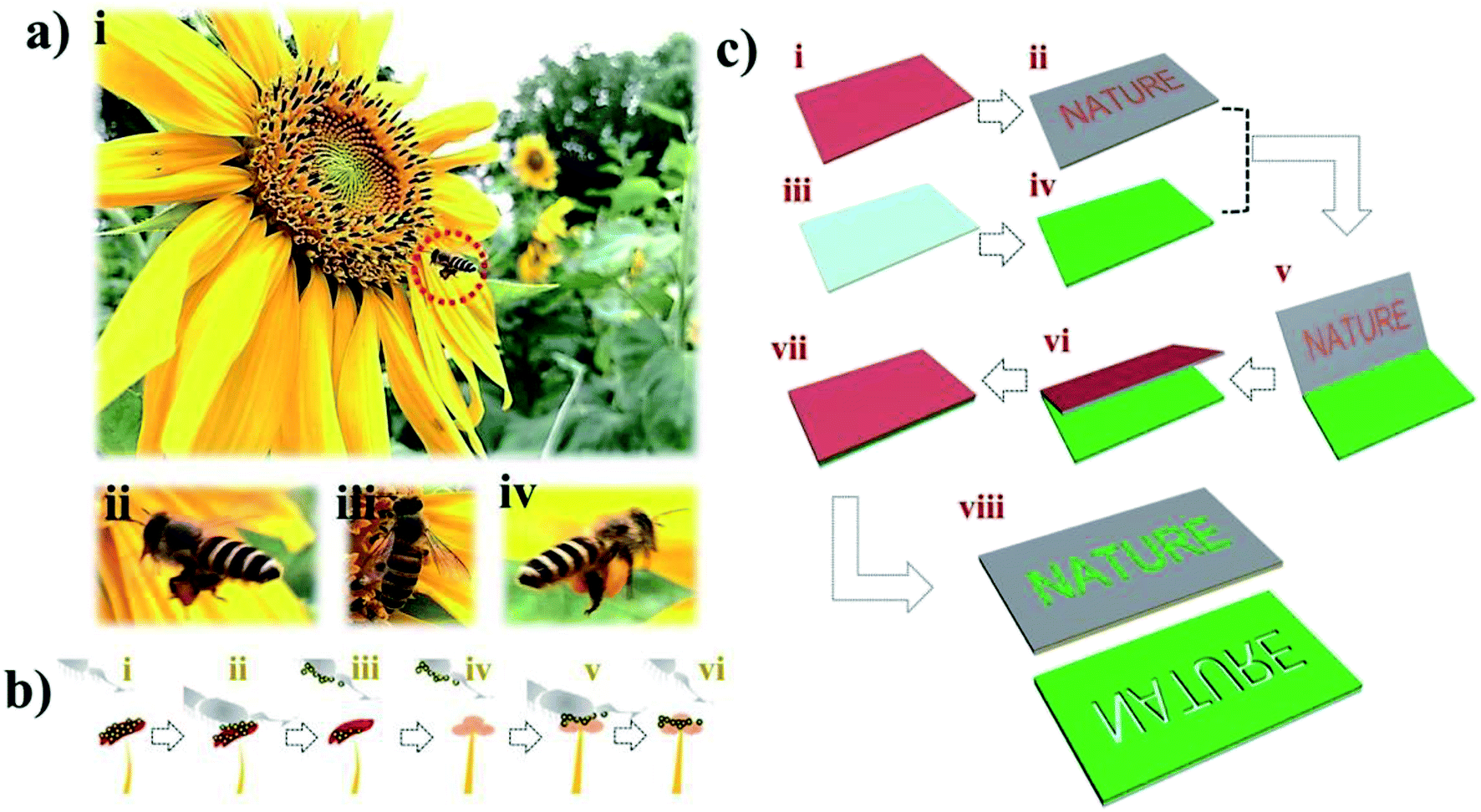 | ||
| Scheme 1 Schematic illustrations of the transfer printing method inspired by bees transferring pollens among flowers. (a) Photographs of the transfer process by bees. (i) A bee collects pollen from a sunflower. (ii) It flies to the first sunflower. (iii) Pollen was collected from the flower (the pollen adhered to its feet). (iv) This bee then flies to another sunflower. (b) Schematic illustration of the process of transferring pollen by bees. (i) A bee flies to a sunflower. (ii) It collects pollen from this flower. (iii) It flies away with pollen adhered to its feet. (iv) The bee then flies to another sunflower. (v) It transfers the pollen on its feet to this second sunflower. (vi) After finishing the pollen transfer process, the bee flies away. (c) Schematic illustration of our proposed transferring method. (i) A tape was treated in a plasma cleaner to increase its surface hydrophilicity. (ii) Toners were printed on the tape to form the pattern template. (iii) A hydrophilic Si/SiO2 substrate was acquired. (iv) Blade coating of the suspension on the Si/SiO2 substrate was used to fabricate the film of the material. (v) and (vi) The patterned tapes and material films were bound and attached to each other. (vii) The tape was contacted with the film of material on the Si/SiO2 substrate and peeled off. (viii) The pattern was fabricated on the substrate of the pattern template on the tape by transfer printing. | ||
2 Experimental section
2.1 Materials
Microcrystalline cellulose, the colorimetric protein assay kit was obtained from Sinopharm Chemical Reagent Co., Ltd. (Shanghai, China). The colorimetric glucose assay kit was purchased from Sigma-Aldrich. Rhodamine B was purchased from Aladdin Bio-Chem Technology Co., Ltd. An oily slurry of conductive graphene was purchased from Nanjing XFNANO Materials Tech Co., Ltd. The monodisperse silica nanoparticles with diameters of 215, 225 and 288 nm were obtained from Nanjing Nanorainbow Biotechnology Co., Ltd. All reagents were of the best grade available and were used as received. All solutions were prepared with deionized water, which was prepared using a Millipore Milli-Q system (resistivity of 18.0 MΩ cm−1).2.2 Experimental procedures
First, suspensions of cellulose, PhCs and graphene were prepared to fabricate the films on the surface of the Si/SiO2 substrate. Each suspension was drop cast onto the Si/SiO2 substrate, and a smooth blade of hard rubber was used to coat the suspension onto the substrate. The suspension was selectively deposited onto the Si/SiO2 surface after blade coating. Next, the tapes were treated in a plasma cleaner (DT-01, Opsplasma, China) to increase their surface hydrophilicity (2 min, 100 W). Toners were printed on the tape substrate to form the pattern template using an office laser printer (CP105b, Fuji Xerox). Then, the tape was contacted with the film of material on the Si/SiO2 substrate and torn off. Finally, the film on the Si/SiO2 substrate was easily transferred onto the patterned tape using the transfer printing method. Due to the hydrophobicity of the toner printed on the substrate, the transferred film of material was restricted to the hydrophilic wells surrounded by the printed toner. Patterned devices were obtained, and SEM (Hitachi S-3000N, Japan) was used to determine their microstructure.Patterned structures were prepared by using the transfer printing method to form defined hydrophilic areas separated by regions of hydrophobic toner. Tape was selected as the substrate, and it was treated with plasma to form hydrophilic areas, and then patterns were printed on the top of the treated tape. After transfer printing, these patterns provide spatial control of the fluids. Moreover, due to capillary action in the millimeter-sized channels, fluid transport can be achieved without pumping. For the cellulose pattern, the glucose and total protein assays were selected to highlight the applicability of the method. All of the reagents from the assay kits were prepared according to the instructions of the kit manufacturer. For the pattern of PhCs, rhodamine B was utilized to show the fluorescence enhancement property of the photonic material. For the graphene pattern, an electronic circuit was fabricated to demonstrate its practical applicability. The recommended peel strength was ranged from 20N/M (conventional transparent tape) to 500N/M (3M VHB tape), since lower peel strength failed to attach nano/micro materials efficiently and higher peel strength caused tape stuck in printers. The thickness of substrates should lower than 200 μm since thicker substrates also caused printer jams.
3 Results and discussion
In this work, we fabricated different patterned devices based on the transfer printing method. A schematic illustration of the fabrication processes is shown in Scheme 1. In detail, the fabrication process includes the following steps. (i) A tape was treated in a plasma cleaner to increase its surface hydrophilicity. (ii) Toners were printed on the tape to form the pattern template. (iii) The suspension was blade coated on the hydrophilic Si/SiO2 substrate. (iv) The tape was contacted with the material film on the Si/SiO2 substrate and peeled off. The material film was transferred onto the substrate of the pattern template. (v) The pattern of the functional material was fabricated on the tape by transfer printing. In our study, we demonstrate the patterning of different materials into different shapes on the tape using the transfer printing method. Successful patterning is based on the adhesion force between the material and the tape being larger than the binding energy between the Si/SiO2 substrate and material. Thus, if they adhere firmly to the tape, then not only cellulose but also PhCs, M. menelaus butterfly wing and graphene can be patterned using this methodology. We can fabricate high-quality printed patterns with this method. In this experiment, a laser printer was used to print the patterns on the tape substrates.32 As shown in Fig. 1, high-quality patterns (hollow circles and channels) with excellent continuity and uniformity can be fabricated on the tapes. As shown in Fig. 1, the diameters of the hollow circles (i, ii, ii and iv) are 305, 400, 503 and 1015 μm, respectively, while the widths of the hollow channels (v, vi, vii and viii) are 232, 310, 417, 494 and 1002 μm, respectively. The hydrophilic hollow circles and channels were defined by hydrophobic barriers comprised of toners. Circle patterns with diameters down to 305 μm and line widths down to 232 μm can easily be achieved with good resolution.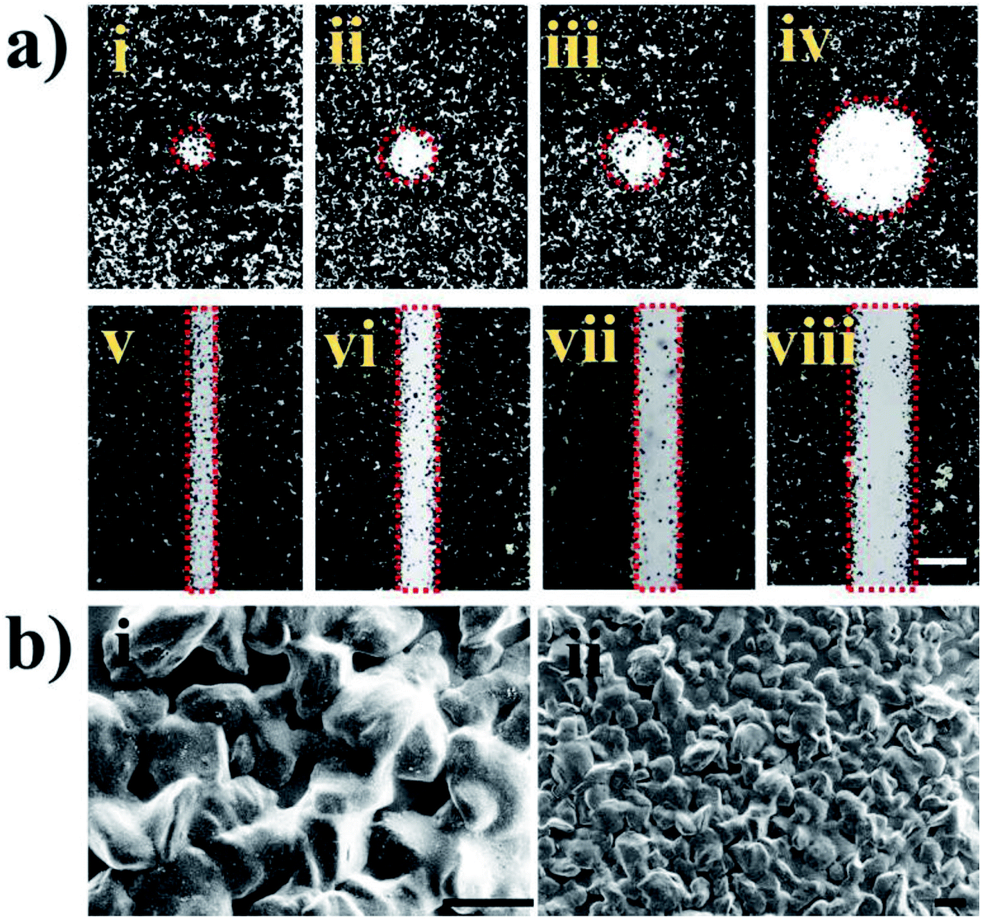 | ||
| Fig. 1 (a) Optical micrographs of the hollow circles (diameters of i, ii, ii and iv are 305, 400, 503 and 1015 μm, respectively) and channels (widths of v, vi, vii and viii are 232, 310, 417, 494 and 1002 μm, respectively) printed on the tape substrates (scale bar: 500 μm). (b) SEM images of the toners printed on the tape substrates under different magnifications (scale bar: 20 μm). | ||
PhC materials, which are created by the self-assembly of monodispersed silica nanoparticles, have many unique optical properties, e.g., a photonic band gap (PBG), a fluorescence enhancement effect, photon localization, and a “slow photon” effect. Due to the extraordinary fluorescent enhancement effect endowed by the slow photon effect, PhCs with controlled micro/nanostructures have shown great potential for applications in many different fields.33,34 As shown in Fig. 2a, silica nanoparticles self-assembled into PhC films and displayed the corresponding colors (blue, green and red), which originated from the periodic photonic structure. Optical photographs and reflection peaks measured for these self-assembled PhCs are shown in Fig. 2a and b. Under normal incidence, the reflection peak positions can be estimated by the Bragg equation, λ = 1.633dnavg, where d is the center-to-center distance between two neighboring silica nanoparticles and navg is the average refractive index of the PhC structure. Using different sizes of silica nanoparticles, PhC films with different reflection peaks and corresponding colors could be obtained by blade coating. In this work, we printed toner onto a tape substrate, which generated the pattern template. Then, the film of the PhCs on the Si/SiO2 substrate was transferred to the pattern template. Finally, the PhCs patterned into different shapes were obtained. As shown in Fig. 2a(iv–vi), the PhC patterns displayed different characteristic colors, which can be generated by self-assembly using silica nanoparticles of different sizes.
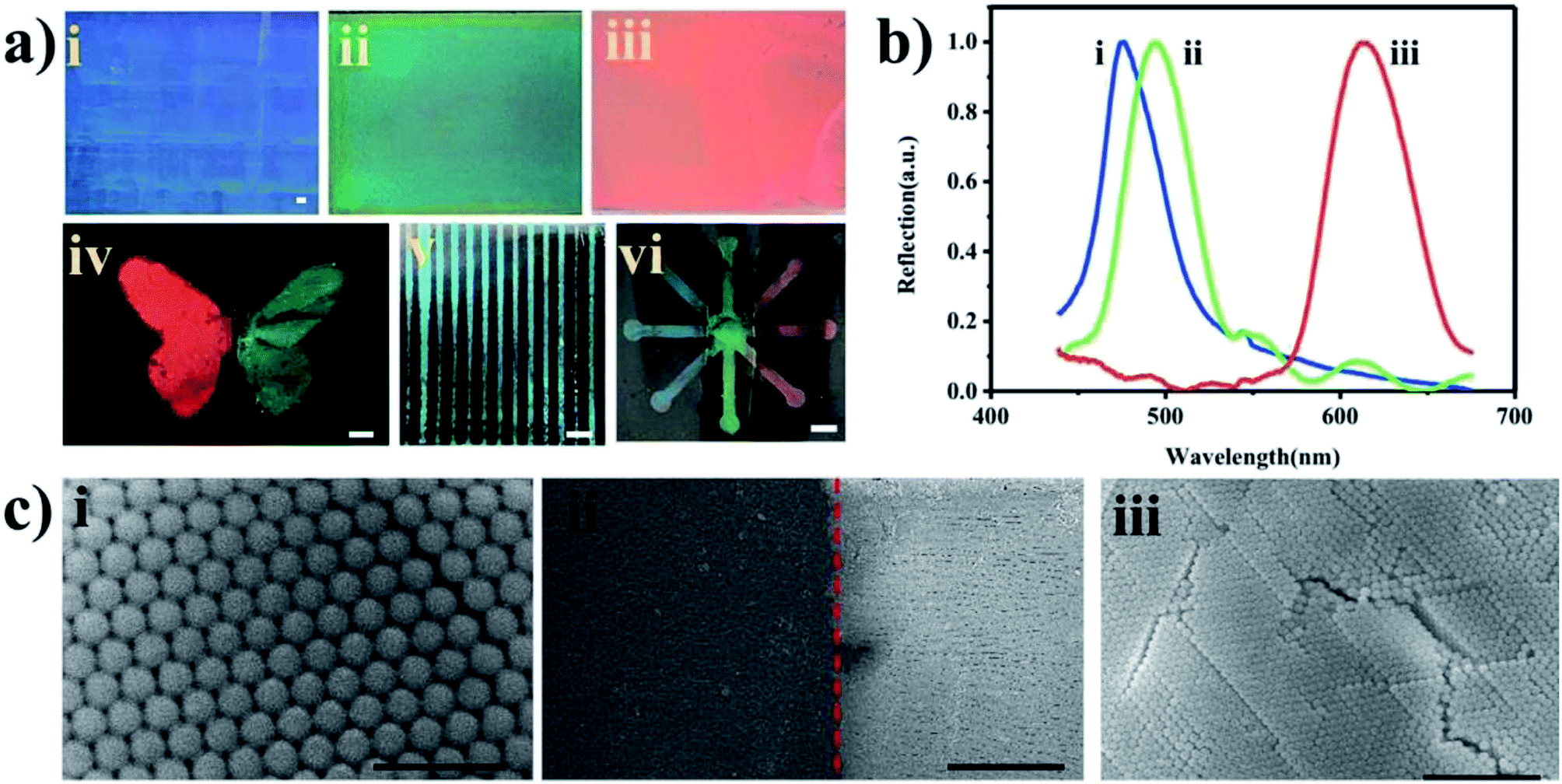 | ||
| Fig. 2 (a) Optical photographs of the PhC films using monodisperse silica nanoparticles with diameters of 215 (i), 225 (ii), and 288 nm (iii) and different patterns (the patterns of iv, v and vi are butterfly, parallel channels and eight channels) fabricated by our developed transfer printing method (scale bar: 20 mm). (b) Reflectance spectra of the PhC films using monodisperse silica nanoparticles with diameters of 215 (i), 225 (ii) and 288 nm (iii). (c) SEM images of the PhCs films (i and iii) and the edge (ii) between the printed toner and the PhC films of the pattern fabricated by the developed transfer printing method (scale bars of i, ii and iii are 1, 500 and 3 μm, respectively). | ||
To demonstrate the applicability of the PhC patterned device, the patterned shape of the PhCs was designed and fabricated for the fluorescent enhancement experiment with rhodamine B, which is widely used in fluorescence bioassays due to its good stability. Rhodamine B has its maximum emission at 590 nm when excited at 550 nm. The PhC microfluidic channels with three branches are shown in Fig. 3(ii). The green reservoir of region A was silica nanoparticles with a diameter of 225 nm. The blue reservoir of region B was silica nanoparticles 215 nm in diameter. The red reservoir of region C was silica nanoparticles 288 nm in diameter. The right reservoir of region D was used for the introduction of rhodamine B. As shown in Fig. 3(iii), the fluorescent image of each reservoir was taken. The fluorescence emission of the red reservoir fabricated using monodisperse silica nanoparticles (288 nm in diameter) was higher than that of the other two reservoirs. Because the maximum fluorescence emission of rhodamine B is at 590 nm, which overlaps with the reflection peak of the nanostructure assembled from silica nanoparticles (288 nm in diameter) (Fig. 3), the fluorescent enhancement was larger than those seen with self-assembled silica nanoparticles 215 nm and 225 nm in diameter. The red reservoir fabricated by monodisperse silica nanoparticles (288 nm in diameter) showed fluorescent signal enhancements of 140-fold and 3-fold compared with the blank and PhC 215 nm reservoirs, respectively. The fluorescence signal can be significantly amplified as a result of the slow photon effect. This amplification mainly occurs because the slow photon effect, which causes the group velocity of photons near the band edge of the photonic stop band in the PhCs to slow down, can improve the effective optical path length of the light, enhancing the interactions between the light and matter.35,36
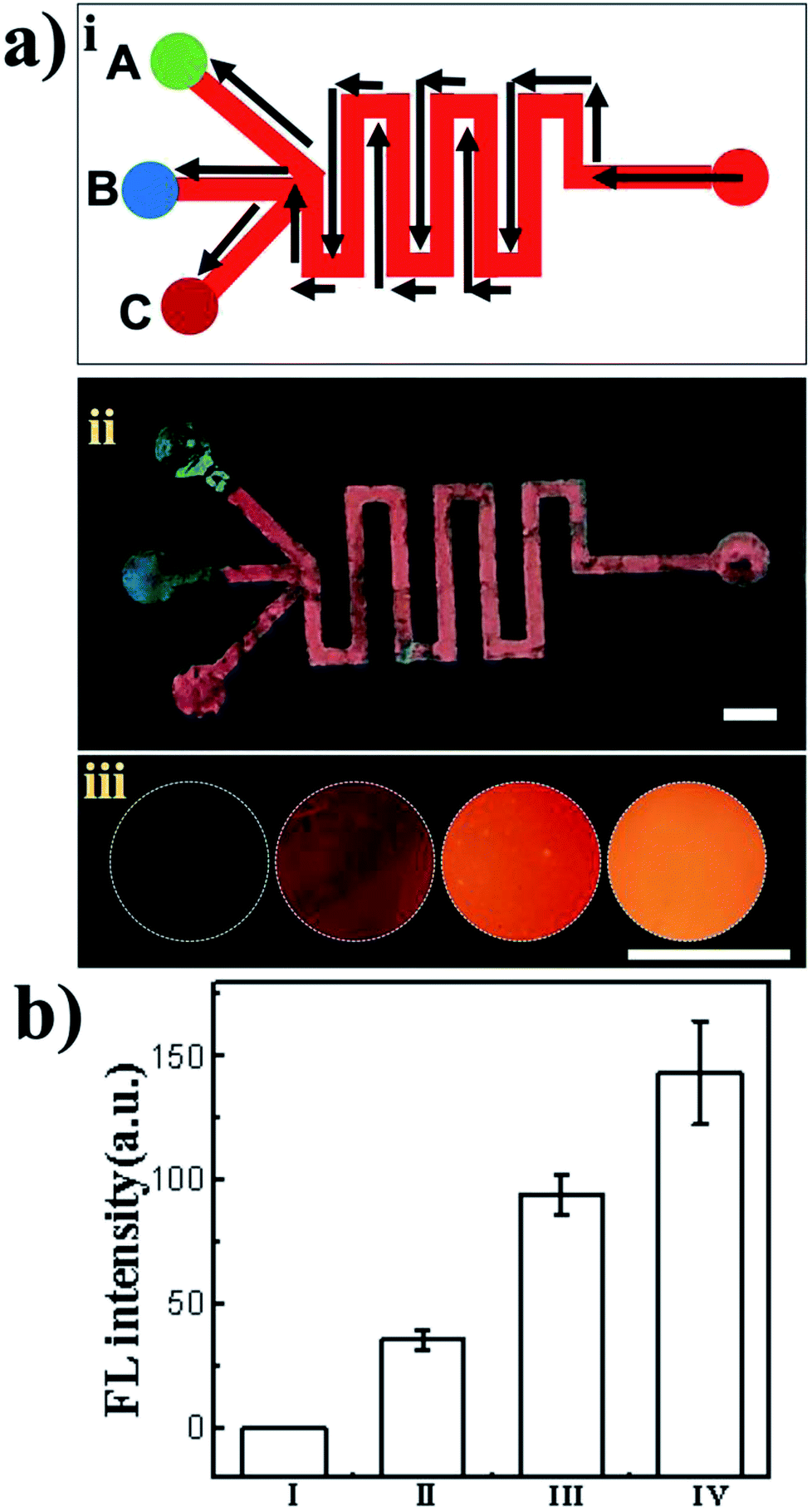 | ||
| Fig. 3 (a) (i) Schematic diagram of the PhC microfluidic channels with three branches (the flow directions in the channels are indicated by black arrows). (ii) Optical image of the PhC microfluidic channels. Channels, region C and region D were fabricated by monodisperse silica nanoparticles with diameters of 288 nm. Region A and region B were fabricated using monodisperse silica nanoparticles with diameters of 215 and 225 nm, respectively (scale bar: 2 mm). (iii) Fluorescence images and fluorescent signals obtained by introduction of rhodamine B (scale bar: 2 mm). Error bars represent the standard deviation for three replicate tests. (b) (I) Blank control, no fluorescent signal. (II) PhC 215, low fluorescent signal. (III) PhC 225, high fluorescent signal. (IV) PhC 288, higher fluorescent signal. | ||
We made patterned cellulose analytical devices based on the transfer printing method. The Y-shaped toner pattern was first printed on a hydrophilic tape as a hydrophobic template. Then, the film of cellulose microfibers was transferred onto the tape template. Due to capillary action in the millimeter-sized channels, the cellulose transfer pattern provided spatial control of fluids and enabled fluid transport without pumping. Moreover, the patterned device allowed multiple assays to be run using a single sample. To demonstrate the applicability of the fabricated analytical device for multiplexed colorimetric assays, the Y-shaped pattern was designed as an analytical device for assaying glucose and protein. The principle of the glucose assay is as follows: first, glucose oxidase catalyzes the oxidation of glucose to release H2O2; second, horseradish peroxidase catalyzes and the oxidation of o-dianisidine by H2O2 to produce brown compounds.37 The detection of BSA is based on a bicinchoninic acid assay, in which peptide bonds present in BSA reduce Cu2+ to Cu+ resulting in a purple-colored chelate complex. The measurement of total proteins is based on a bicinchoninic acid assay. Peptide bonds in proteins can reduce Cu2+ to Cu+ and generate purple chelate complexes. When loading samples on A, liquid flow separately from A to BCD as they are three branched channels with same materials in channels.
As shown in Fig. 4a(ii and iii), the inlet of the sample is the central reservoir (region A), which was used to introduce analytes containing glucose and protein. The reservoirs of region B, region C and region D were the detection areas for the control, glucose and total protein, respectively. Specifically, 0.8 μL of standard solution containing glucose and protein at known concentrations was injected into region A and flow into the detection areas. When eject sample containing glucose and BSA was injected in A, BSA and glucose flow together to BCD separately, C and D presented different color because they were loaded with specific reagents for BSA and glucose sensing before sampling. Then, the colors were observed after 10 min. As the glucose concentration increased, the color changed from colorless to brown, and the intensity of the color change was related to the glucose concentration. For the total protein assay, the color changed from green to purple, and the intensity of the color change was related to the concentration of total proteins. The images in Fig. 4c and d were recorded and transmitted to Adobe Photoshop CS5 to instantly analyze the color data, and the color intensities were obtained from the histogram of the colors in the detection reservoir. As depicted in Fig. 4c and d, the detection ranges for glucose and total protein were from 2.5 to 200 mM and 5 to 75 μM, respectively.
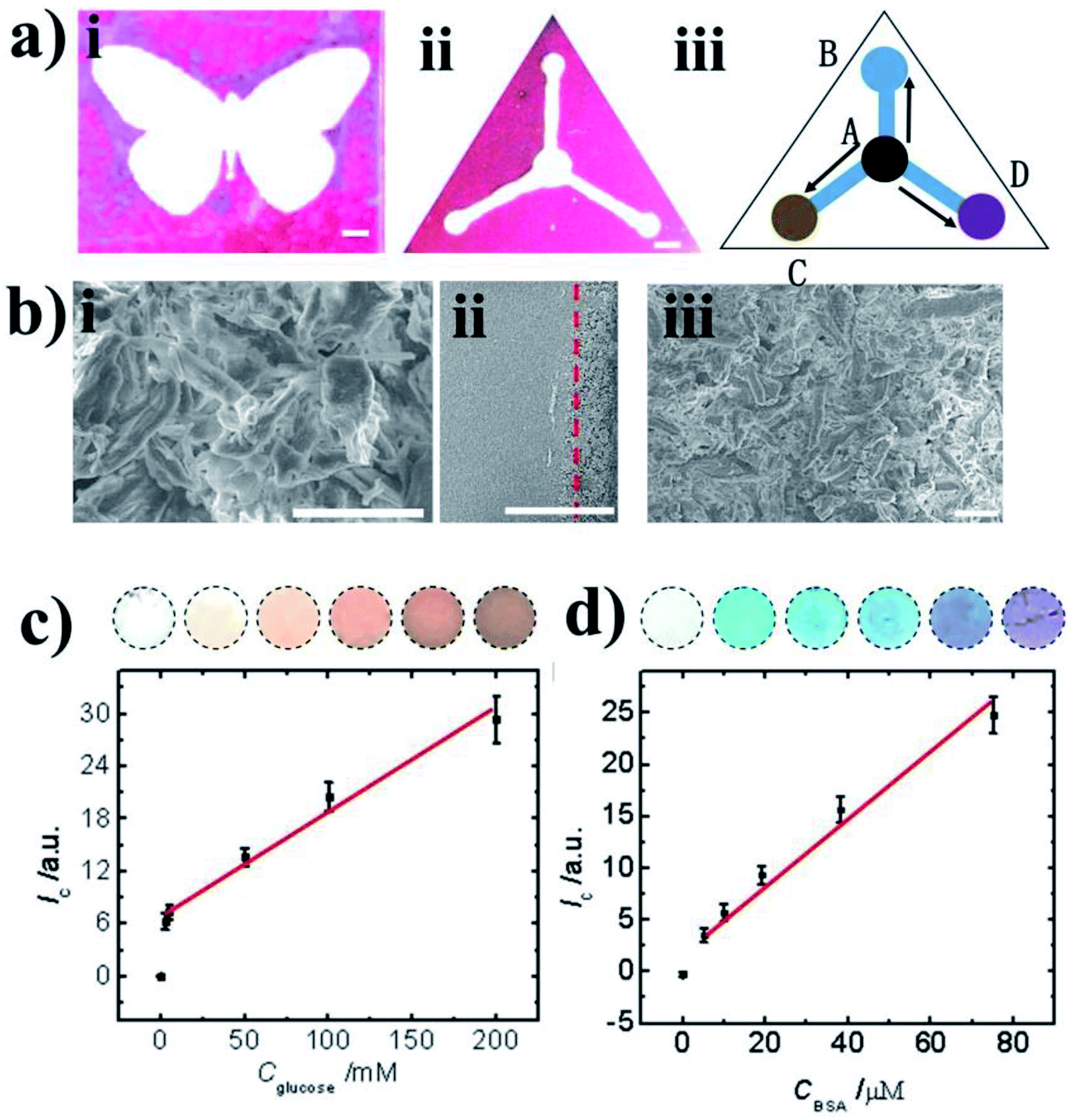 | ||
| Fig. 4 (a) Optical image ((i), (ii), scale bar: 2 mm) and schematic diagram (iii) of cellulose transfer patterns; (A) reservoir as an inlet for sample introduction, (B) reservoir for blank control, (C) detection area for the glucose assay, (D) detection area for the total protein assay. The flow directions in the channels are indicated by black arrows. (b) SEM images of the cellulose films ((i) before transfer, (iii) after transfer, scale bar: 20 μm) and the edge ((ii) scale bar: 1 mm) between the printed toner and the cellulose films of the pattern fabricated by the developed transfer printing method. (c) Colorimetric signals as a function of glucose concentration. (d) Colorimetric signals as a function of protein concentration. Error bars represent the standard deviation for three replicate tests. | ||
In the biological world, the brilliant colors exhibited by butterfly wings are derived from multilayered micro/nanostructures, which can be used as templates for fabricating a rich variety of photonic-related structures or devices. There are a wide variety of applications, such as gas sensors, surface-enhanced Raman spectroscopy, microfluidics, and surface plasmon resonance technologies, inspired by butterfly wings with bright colors and natural periodic structures.38,39 The multifunctional nature of M. menelaus butterfly wings, which are lightweight, hydrophobic, mechanically strong, photoresponsive and thermoresponsive, is achieved due to the elaborated photonic nanostructures in the ridges of the scales. As shown in Fig. 5a, M. menelaus wing can be successfully transferred onto the patterned tape, which can then be used to fabricate detection devices as our group previously reported.40 Scanning electron microscopy (SEM) images (Fig. 5b) show the structure of the M. menelaus wing ((i) – before transfer, (iii) – after transfer). The directions of the M. menelaus butterfly wings on the left and right sides (Fig. 5a(ii)) are different, indicating that the butterfly wings can be transferred onto the pattern in different directions.
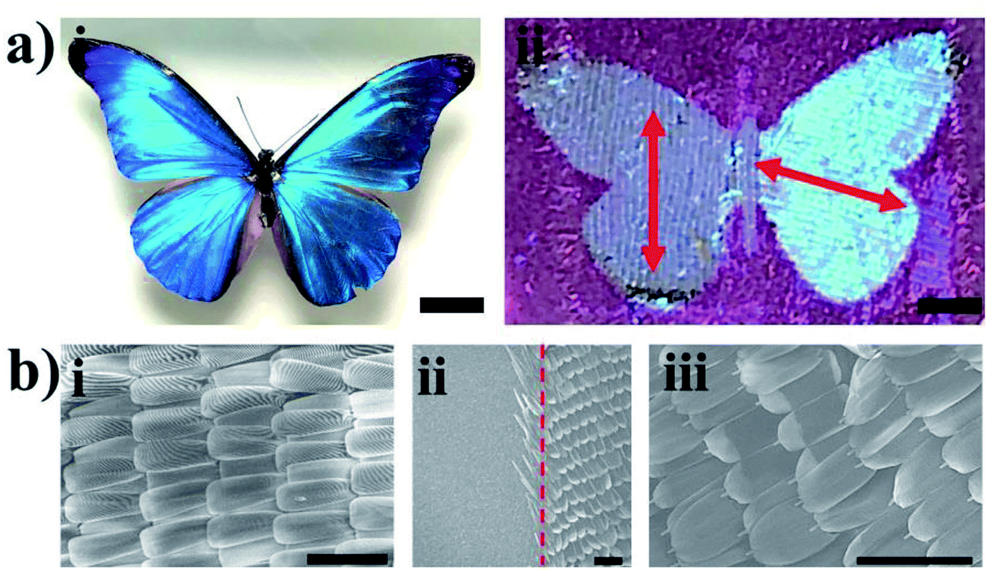 | ||
| Fig. 5 (a) An optical photograph of M. menelaus ((i) scale bar: 2 cm) and the butterfly pattern prepared by transferring the wing of M. menelaus in different directions ((ii) scale bar: 2 mm). (b) SEM image of the M. menelaus wing ((i) before transfer and (iii) after transfer). Panel (ii) shows the edge between the printed toner (left side of the red line) and the M. menelaus wing (right side of the red line) (scale bar: 200 μm). | ||
With the office laser printer we used, the designed patterns could be printed on tapes with excellent continuity and uniformity. The graphene film can be precisely transferred onto the tape template to form high-quality graphene patterns. Fig. 6a shows the optical images of the graphene patterns. The morphology of the patterned graphene is displayed in the SEM images in Fig. 6b. Moreover, these patterns can be used to make a variety of functional circuits and devices. As a demonstration of the practical applications of such patterns, a simple electronic circuit using patterned graphene was prepared, as shown in Fig. 6c. The circuit was composed of a 5.0 V battery, patterned graphene and an LED. The patterned graphene worked rather well as a normal electronic circuit connected in series with a battery and an LED. Fig. 6c shows photographs of the graphene circuit in the ON/OFF states of the LED, which demonstrated that this is an effective approach for creating high-conductivity graphene patterns.
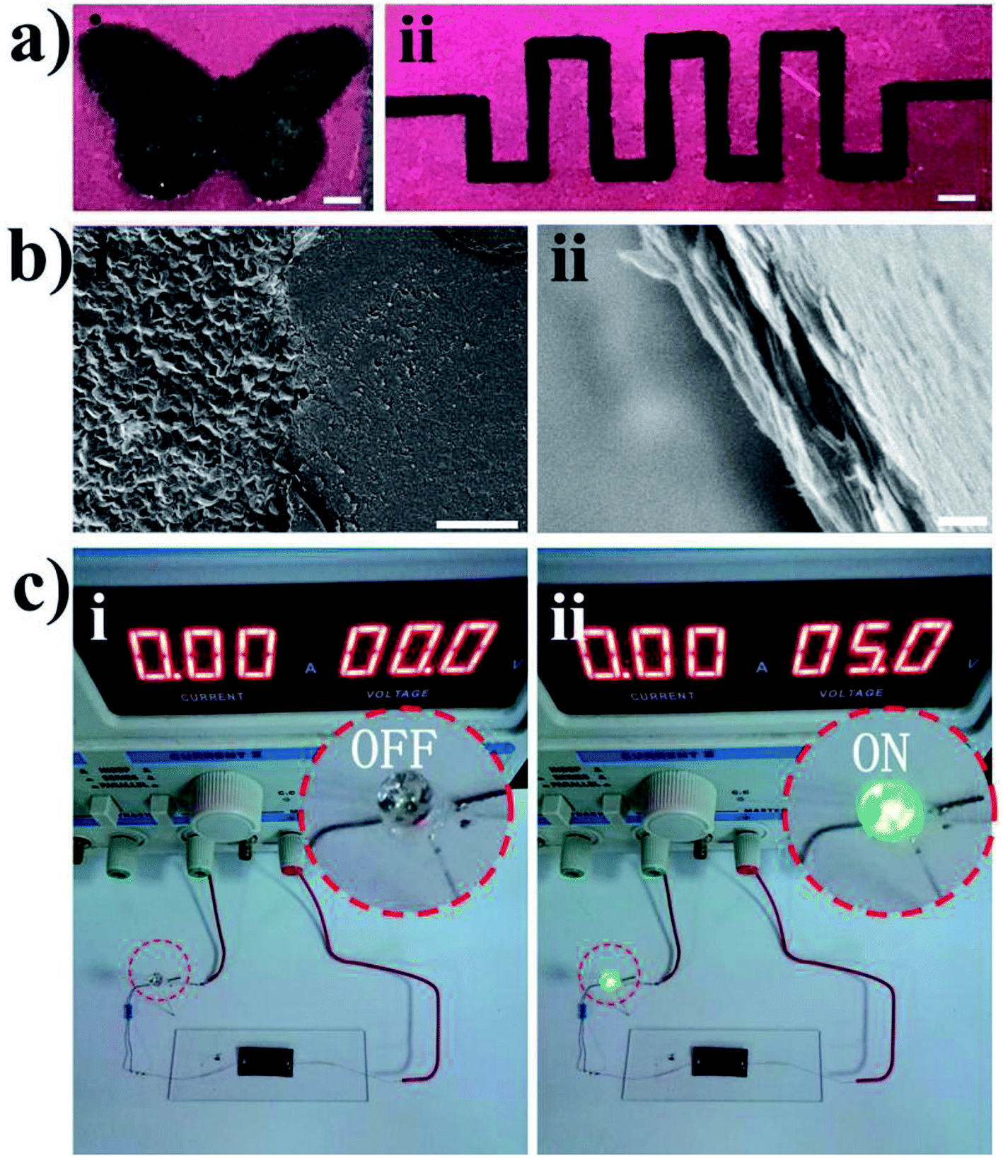 | ||
| Fig. 6 (a) Optical photographs of different graphene patterns fabricated by our developed transfer printing method ((i) pattern of a butterfly, (ii) pattern of a wavy line). (b) SEM images of the graphene film (i) and cross section of the graphene film (ii). (c) Optical photographs of the circuit with the battery showing the ON/OFF states of the LED. | ||
4 Conclusion
In summary, we report a simple, reliable, low-cost and practical patterning method to transfer different materials onto tapes with the transfer printing method. Using this method, various patterned templates can be printed on the tapes, and different materials (cellulose, PhCs, M. menelaus wing and graphene) can be transferred. The proposed technique is a simple and controllable methodology with many advantages, including being both less expensive and less destructive. These advantages make this approach very useful for creating different patterns, and we expect these patterns to have broad applications in biomedical devices and biosensors. We believe that these patterned structures will prove promising for a wide variety of applications.Conflicts of interest
There are no conflicts to declare.Acknowledgements
We gratefully acknowledge financial support from the Natural Science Foundation of Jiangsu Province of China (Grant No. BK20171025 and BK20150954), the National Natural Science Foundation of China (Grant No. 51506081, 81803274 and 21635001), the University Natural Science Research Project in Jiangsu Province (Grant No. 16KJB330001), the Postdoctoral Science Foundation of China and Jiangsu Province (Grant No. 2016M601797, 2017M621597, 2018T110428 and 1701182C), the Key Research and Development Plan of Jiangsu Province (BE2016002), the Project of Special Funds of Jiangsu Province for the Transformation of Scientific and Technological Achievements (BA2015067), the 111 Project (B17011, Ministry of Education of China).References
- K. Zhong, J. Li, L. Liu, S. V. Cleuvenbergen, K. Song and K. Clays, Instantaneous, Simple, and Reversible Revealing of Invisible Patterns Encrypted in Robust Hollow Sphere Colloidal Photonic Crystals, Adv. Mater., 2018, 30, 1707246 CrossRef PubMed.
- L. Zhang, H. Liu, Y. Zhao, X. Sun, Y. Wen, Y. Guo, X. Gao, C. A. Di, G. Yu and Y. Liu, Inkjet Printing High-Resolution, Large-Area Graphene Patterns by Coffee-Ring Lithography, Adv. Mater., 2012, 24, 436–440 CrossRef CAS PubMed.
- B. Gao, H. Liu and Z. Gu, Bottom-Up Fabrication of Paper-Based Microchips by Blade Coating of Cellulose Microfibers on a Patterned Surface, Langmuir, 2014, 30, 15041–15046 CrossRef CAS PubMed.
- C. Ingrosso, V. Fakhfouri, M. Striccoli, A. Agostiano, A. Voigt, G. Gruetzner, M. L. Curri and J. Brugger, An Epoxy Photoresist Modified by Luminescent Nanocrystals for the Fabrication of 3D High-Aspect-Ratio Microstructures, Adv. Funct. Mater., 2007, 17, 2009–2017 CrossRef CAS.
- Y. Zhou and K. P. Loh, Making Patterns on Graphene, Adv. Mater., 2010, 22, 3615–3620 CrossRef CAS PubMed.
- Z. Huang, M. Su, Q. Yang, Z. Li, S. Chen, Y. Li, X. Zhou, F. Li and Y. Song, A general patterning approach by manipulating the evolution of two-dimensional liquid foams, Nat. Commun., 2017, 8, 14110 CrossRef CAS PubMed.
- Z. Huang, Q. Yang, M. Su, Z. Li, X. Hu, Y. Li, Q. Pan, W. Ren, F. Li and Y. Song, A General Approach for Fluid Patterning and Application in Fabricating Microdevices, Adv. Mater., 2018, 30, 1802172 CrossRef PubMed.
- L. Zhang, D. DeArmond, N. T. Alvarez, R. Malik, N. Oslin, C. McConnell, P. K. Adusei, Y. Y. Hsieh and V. Shanov, Flexible Micro-Supercapacitor Based on Graphene with 3D Structure, Small, 2017, 13, 1603114 CrossRef PubMed.
- J. Ye, H. Tan, S. Wu, K. Ni, F. Pan, J. Liu, Z. Tao, Y. Qu, H. Ji and P. Simon, Direct Laser Writing of Graphene Made from Chemical Vapor Deposition for Flexible, Integratable Micro-Supercapacitors with Ultrahigh Power Output, Adv. Mater., 2018, 30, 1801384 CrossRef PubMed.
- M. Beidaghi and C. Wang, Micro-Supercapacitors Based on Interdigital Electrodes of Reduced Graphene Oxide and Carbon Nanotube Composites with Ultrahigh Power Handling Performance, Adv. Funct. Mater., 2012, 22, 4501–4510 CrossRef CAS.
- M. S. Alias, Y. Yang, T. K. Ng, I. Dursun, D. Shi, M. I. Saidaminov, D. Priante, O. M. Bakr and B. S. Ooi, Enhanced Etching, Surface Damage Recovery, and Submicron Patterning of Hybrid Perovskites Using a Chemically Gas-Assisted Focused-Ion Beam for Subwavelength Grating Photonic Applications, J. Phys. Chem. Lett., 2015, 7, 137–142 CrossRef PubMed.
- R. F. Tiefenauer, K. Tybrandt, M. Aramesh and J. Vörös, Fast and Versatile Multiscale Patterning by Combining Template-Stripping with Nanotransfer Printing, ACS Nano, 2018, 12, 2514–2520 CrossRef CAS PubMed.
- N. Kim, H. Kang, J. H. Lee, S. Kee, S. H. Lee and K. Lee, Highly Conductive All-Plastic Electrodes Fabricated Using a Novel Chemically Controlled Transfer-Printing Method, Adv. Mater., 2015, 27, 2317–2323 CrossRef CAS PubMed.
- H. Yi, M. Seong, K. Sun, I. Hwang, K. Lee, C. Cha, T. I. Kim and H. E. Jeong, Wet-Responsive, Reconfigurable, and Biocompatible Hydrogel Adhesive Films for Transfer Printing of Nanomembranes, Adv. Funct. Mater., 2018, 28, 1706498 CrossRef.
- L. A. Garibaldi, I. Steffan-Dewenter, R. Winfree, M. A. Aizen, R. Bommarco, S. A. Cunningham, C. Kremen, L. G. Carvalheiro, L. D. Harder, O. Afik, I. Bartomeus, F. Benjamin, V. Boreux, D. Cariveau, N. P. Chacoff, J. H. Dudenhöffer, B. M. Freitas, J. Ghazoul, S. Greenleaf, J. Hipólito, A. Holzschuh, B. Howlett, R. Isaacs, S. K. Javorek, C. M. Kennedy, K. M. Krewenka, S. Krishnan, Y. Mandelik, M. M. Mayfield, I. Motzke, T. Munyuli, B. A. Nault, M. Otieno, J. Petersen, G. Pisanty, S. G. Potts, R. Rader, T. H. Ricketts, M. Rundlöf, C. L. Seymour, C. Schüepp, H. Szentgyörgyi, H. Taki, T. Tscharntke, C. H. Vergara, B. F. Viana, T. C. Wanger, C. Westphal, N. Williams and A. M. Klein, Wild Pollinators Enhance Fruit Set of Crops Regardless of Honey Bee Abundance, Science, 2013, 339, 1608–1611 CrossRef CAS PubMed.
- B. Marzinzig, L. Brünjes, S. Biagioni, H. Behling, W. Link and C. Westphal, Bee Pollinators of Faba Bean (Vicia faba L.) Differ in their Foraging Behaviour and Pollination Efficiency, Agric., Ecosyst. Environ., 2018, 264, 24–33 CrossRef.
- D. Klemm, F. Kramer, S. Moritz, T. Lindström, M. Ankerfors, D. Gray and A. Dorris, Nanocelluloses: A New Family of Nature-Based Materials, Angew. Chem., Int. Ed., 2011, 50, 5438–5466 CrossRef CAS PubMed.
- E. Lam, K. B. Male, J. H. Chong, A. C. Leung and J. H. Luong, Applications of Functionalized and Nanoparticle-Modified Nanocrystalline Cellulose, Trends Biotechnol., 2012, 30, 283–290 CrossRef CAS PubMed.
- R. J. Moon, A. Martini, J. Nairn, J. Simonsen and J. Youngblood, Cellulose Nanomaterials Review: Structure, Properties and Nanocomposites, Chem. Soc. Rev., 2011, 40, 3941–3994 RSC.
- R. A. Potyrailo, H. Ghiradella, A. Vertiatchikh, K. Dovidenko, J. R. Cournoyer and E. Olson, Morpho Butterfly Wing Scales Demonstrate Highly Selective Vapour Response, Nat. Photonics, 2007, 1, 123 CrossRef CAS.
- A. D. Pris, Y. Utturkar, C. Surman, W. G. Morris, A. Vert, S. Zalyubovskiy, T. Deng, H. T. Ghiradella and R. A. Potyrailo, Towards High-Speed Imaging of Infrared Photons with Bio-Inspired Nanoarchitectures, Nat. Photonics, 2012, 6, 195 CrossRef CAS.
- M. Zhang, J. Meng, D. Wang, Q. Tang, T. Chen, S. Rong, J. Liu and Y. Wu, Biomimetic Synthesis of Hierarchical 3D Ag Butterfly Wing Scale Arrays/Graphene Composites as Ultrasensitive SERS Substrates for Efficient Trace Chemical Detection, J. Mater. Chem. C, 2018, 6, 1933–1943 RSC.
- J. Hou, M. Li and Y. Song, Patterned Colloidal Photonic Crystals, Angew. Chem., Int. Ed., 2018, 57, 2544–2553 CrossRef CAS PubMed.
- Z. Yu, C. F. Wang, L. Ling, L. Chen and S. Chen, Triphase Microfluidic-Directed Self-Assembly: Anisotropic Colloidal Photonic Crystal Supraparticles and Multicolor Patterns Made Easy, Angew. Chem., 2012, 124, 2425–2428 CrossRef.
- T. Ding, S. K. Smoukov and J. J. Baumberg, Stamping Colloidal Photonic Crystals: A Facile Way Towards Complex Pixel Colour Patterns for Sensing and Displays, Nanoscale, 2015, 7, 1857–1863 RSC.
- K. Chen, Q. Fu, S. Ye and J. Ge, Multicolor Printing Using Electric-Field-Responsive and Photocurable Photonic Crystals, Adv. Funct. Mater., 2017, 27, 1702825 CrossRef.
- S. Ye, Q. Fu and J. Ge, Invisible Photonic Prints Shown by Deformation, Adv. Funct. Mater., 2014, 24, 6430–6438 CrossRef CAS.
- Q. Zhuo, Q. Wang, Y. Zhang, D. Zhang, Q. Li, C. Gao, Y. Sun, L. Ding, Q. Sun and S. Wang, Transfer-Free Synthesis of Doped and Patterned Graphene Films, ACS Nano, 2015, 9, 594–601 CrossRef CAS PubMed.
- A. K. Geim, Graphene: Status and Prospects, Science, 2009, 324, 1530–1534 CrossRef CAS PubMed.
- K. S. Kim, Y. Zhao, H. Jang, S. Y. Lee, J. M. Kim, K. S. Kim, J. H. Ahn, P. Kim, J. Y. Choi and B. H. Hong, Large-Scale Pattern Growth of Graphene Films for Stretchable Transparent Electrodes, Nature, 2009, 457, 706–710 CrossRef CAS PubMed.
- L. Huang, Y. Huang, J. Liang, X. Wan and Y. Chen, Graphene-Based Conducting Inks for Direct Inkjet Printing of Flexible Conductive Patterns and their Applications in Electric Circuits and Chemical Sensors, Nano Res., 2011, 4, 675–684 CrossRef CAS.
- J. Chi, B. Gao, M. Sun, F. Zhang, E. Su, H. Liu and Z. Gu, Patterned Photonic Nitrocellulose for Pseudopaper Elisa, Anal. Chem., 2017, 89, 7727–7733 CrossRef CAS PubMed.
- K. R. Phillips, G. T. England, S. Sunny, E. Shirman, T. Shirman, N. Vogel and J. Aizenberg, A Colloidoscope of Colloid-Based Porous Materials and their Uses, Chem. Soc. Rev., 2016, 45, 281–322 RSC.
- Y. Tan, T. Tang, H. Xu, C. Zhu and B. T. Cunningham, High Sensitivity Automated Multiplexed Immunoassays Using Photonic Crystal Enhanced Fluorescence Microfluidic System, Biosens. Bioelectron., 2015, 73, 32–40 CrossRef CAS PubMed.
- B. Gao, L. Tang, D. Zhang, Z. Xie, E. Su, H. Liu and Z. Gu, Transpiration-Inspired Fabrication of Opal Capillary with Multiple Heterostructures for Multiplex Aptamer-Based Fluorescent Assays, ACS Appl. Mater. Interfaces, 2017, 9, 32577–32582 CrossRef CAS PubMed.
- B. Gao, H. Liu and Z. Gu, Patterned Photonic Nitrocellulose for Pseudo-Paper Microfluidics, Anal. Chem., 2016, 88, 5424–5429 CrossRef CAS.
- H. Liu, X. Li and R. M. Crooks, Based Slippad for High-Throughput Chemical Sensing, Anal. Chem., 2013, 85, 4263–4267 CrossRef CAS PubMed.
- E. S. A. Goerlitzer, R. N. K. Taylor and N. Vogel, Bioinspired Photonic Pigments from Colloidal Self-Assembly, Adv. Mater., 2018, 30, 1706654 CrossRef PubMed.
- Q. Shen, Z. Luo, S. Ma, P. Tao, C. Song, J. Wu, W. Shang and T. Deng, Bioinspired Infrared Sensing Materials and Systems, Adv. Mater., 2018, 30, 1707632 CrossRef PubMed.
- Z. He, A. Elbaz, B. Gao, J. Zhang, E. Su and Z. Gu, Wearable Biosensors: Disposable Morpho menelaus Based Flexible Microfluidic and Electronic Sensor for the Diagnosis of Neurodegenerative Disease, Adv. Healthcare Mater., 2018, 7, 1870025 CrossRef.
| This journal is © The Royal Society of Chemistry 2019 |