
 Open Access Article
 This Open Access Article is licensed under a Creative Commons Attribution-Non Commercial 3.0 Unported Licence
First principles study for band engineering of KNbO3 with 3d transition metal substitution†
Yunting Liang abc and
Guosheng Shao*abc
abc and
Guosheng Shao*abc
aSchool of Materials Science and Engineering, Zhengzhou University, Zhengzhou 450001, China. E-mail: gsshao@zzu.edu.cn
bState Center for International Cooperation on Designer Low-carbon & Environmental Materials (CDLCEM), Zhengzhou University, 100 Kexue Avenue, Zhengzhou 450001, China
cZhengzhou Materials Genome Institute (ZMGI), Zhongyuanzhigu, Building 2, Xingyang 450100, China
First published on 6th March 2019
Abstract
First principles calculations in the framework of density functional theory (DFT) were performed to tune the electronic structures of wide gap KNbO3 through 3d transition metal substitution, using PBE and HSE06 functionals for the exchange correlation potentials. While PBE functionals are suitable for structural and energetic properties, HSE06 is more reliable for band structure calculations. Impurity bands owing to V, Mn, or Fe are present in the forbidden gap, leading to effective reduction of optical gaps via multiple wavelength absorption. It is discovered that Ti and Cr doped systems are suitable for n type transparent conducting oxide (TCO), the Ni doped system for highly desirable p type TCO, and the Cu doped system is an excellent candidate for p type optical absorber layers. This work provides a systematic and overall perspective on the effects and associated mechanisms of transition metal doping or alloying, thus helping exploitation of perovskite oxides as potential key materials for photovoltaic and transparent photonic applications.
Introduction
As a most promising renewable energy source to address the energy crisis due to limited fossil fuel resources and related environmental damage, current silicon wafer based solar cells have been extensively exploited for decades, with a maximum energy conversion efficiency of only about 25% due to the Shockley–Queisser (SQ) limit.1,2 Thin film solar cells using hybrid perovskite CH3NH3PbI3 as the optical absorbing layer were shown to be promising as a low-cost technology, with efficiency beyond 22% having been achieved over a short time since initial work in 2009, largely attributed to a suitable bandgap and high carrier mobility.3,4 However, there are two obvious setbacks for CH3NH3PbI3 solar cells, which hinder their wide application. One concern lies in material instability in the ambient environment, and the other comes from potential pollution from lead ions. It is therefore necessary to develop perovskite materials which are stable, abundant and environmentally friendly, thus making them desirable for the next generation of high-performance thin film solar cells.Recently researchers have made further efforts in exploring inorganic perovskite CsPbI3 for photovoltaic application, through tentative substitutions of Pb to avoid toxicity and iodine to address instability issues.5–7 Previous work8–27 suggested that inorganic and nontoxic multiferroic perovskite semiconductors, particularly oxide based systems, could be better alternatives for solar cell applications, owing to their high stability with adjustable bandgap and carrier concentrations through doping or alloying. Generally, a typical wide gap perovskite is based on the configuration of ABO3, with A being an alkaline-earth metal or alkali metal element and B a transition metal. Generally, d-orbitals from the B site defines the position of the conduction band minimum (CBM) and oxygen 2p states sitting at the valence band maximum (VBM). Such a rule of thumb has been widely exploited, leading to effective doping or alloying in ATiO3 (A = Ca, Sr and Ba),8–13 KNbO3 (ref. 14, 15 and 18–27) and BiFeO3.16,17
Among these oxide perovskites, effective alloying or doping effect was achieved in KNbO3 (for the sake of simplicity, we use doping to refer incorporation of impurity element in this work). As is well recognized, first principle studies can provide very useful insights on alloying or doping effects, so that effective tuning of fundamental electronic structures and associated properties can be realized cost effectively through fundamental guidance.18 Grinberg et al.19 modelled alloying effect in [KNbO3]1−x[BaNi1/2Nb1/2O3−δ]x, namely KBNNO, and then prepared materials with x = 0.1–0.5 to obtain bandgaps of 1.1–2.0 eV suitable for solar cells. Their theoretical calculations revealed that the filled Ni 3d states at the VBM played a crucial role in lowering the bandgap, which was confirmed by their experimental work. Subsequent experimental work by Zhou et al.20 showed with XRD analysis that the KBNNO crystals underwent phase transitions from orthorhombic to cubic structure with x increasing from 0 to 0.3. Their UV experiment showed the same range of reduced bandgap with Grinberg's results. They then prepared Ba(Ti0.75Ce0.125Ni0.125)O3−δ (BTCN) thin film that exhibited a cubic perovskite structure, albeit being deviated from the ideal Pm3m space group. They concluded that the Ni octahedral energy splitting in BTCN resulted in bandgap reduction.21 On the basis of the substitutional model by Grinberg et al., various co-doping efforts were then made experimentally, covering Ba + Fe,22 Ba + Co,23,24 Ba + Ni25–27 and Ba + Zn28 in KNbO3, though the impacts of the subsequent work was limited due to the lack of systematic understanding for electronic structures.
Another important component of a thin-film photovoltaic cell is a transparent conductive oxide (TCO), which is typically of a wide bandgap over 3.0 eV with effective doping to deliver high electrical conductivity without losing transmittance to visible and infrared light. As is widely recognized, the current TCO coatings are dominated by Sn-doped indium oxide (ITO), which is expensive with very limited indium resources.29,30 While FTO (F–SnO2) has rivalling TCO performance, there is toxic issue from using fluorine for doping.31 Another candidate AZO (Al–ZnO) suffers from the setback of low material stability.32 Great efforts are therefore needed to deliver alternative TCO candidates using low-cost materials with large and green resources, so that sustainable alternative materials can be used to meet the ever-increasing need of TCO coatings.33 It is envisaged that wide gap perovskite oxides could offer competitive TCO solutions, owing to the large variety of compositional choices and inherited high carrier mobility, although efforts in this regard have been rather limited.34,35
This work is dedicated to provide a fundamental road map in guiding doping oxide perovskite with 3d transition metals. The work covers doping/alloying effect though introduction of each of the 3d elements into BaNb2/3B′1/3O3, so as to obtain a perspective view on the interactive role of d-orbitals towards band engineering. We find that introduction of 3d element demonstrates three distinctive effects: (a) shifting the Fermi level towards either the CBM or the VBM for effective doping into degenerated n- or p-type semiconductors; (b) introduction of mid-gap bands to permit multi-wavelength absorption; and (c) change of bandgap values through alloying.
Method
First principles modelling was carried out in the framework of the density functional theory (DFT), using the Vienna Ab initio Simulation Package code (VASP) with a plane-wave basis set described by the projector augmented wave (PAW) method for the ionic potentials.36 It is well established that functionals from generalized gradient approximation (GGA) underestimate bandgap values for transition metal oxides due to omission of the nonlocal effect, even though they are fundamentally adequate for structure-energy investigation at the ground states (e.g. formation energy, lattice parameters, and semi-quantitatively, as well as magnetism owing to spin polarization).37–41 Here we used the PBE functional42,43 for efficient structure-energy modelling to determine the stable structures of doped/alloyed materials. For dependable band structures, we adopted the well tested HSE06 functionals.44–47 The screen parameter (w) for the HSE06 model is 0.2, which defines a short range (2/w) for mixing of a quarter of HF with PBE for reduced computational cost (no screening corresponds to PBE0). It was shown in previous work that HSE06 was adequate to predict a band gap of 3.10 eV for the orthorhombic KNbO3 perovskite phase,48 being in excellent agreement with the experimental value of 3.23 eV.49An energy cut-off of 520 eV was adopted for the PAW-PBE pseudopotentials, as recommended in the VASP manual (1.3 times of default upper cut-off energy),50 Table S1.† A criterion of 0.01 eV Å−1 per atom was chosen for adequate relaxation of the Hellmann–Feynman residual forces, together with a Gaussian smearing width of 0.05 eV to quicken convergence. The adopted high symmetry paths for cubic KNbO3 were X (0.5, 0, 0), R (0.5, 0.5, 0.5), M (0.5, 0.5, 0), G (0, 0, 0) and R (0.5, 0.5, 0.5). K mesh was defined with spacing below 0.03 Å−1 for structure-energy calculations, and a finer K-mesh was used for electronic structures (spacing below 0.04 Å−1).
The 2 × 2 × 2 super cell of KNbO3 unit cells (40 atoms) was used to study doping effect on the Nb site, with the doping model of solid solution (KNbO3)5/8-(BaNb2/3B′1/3O3)3/8, as shown in Fig. 1. In such a structural model, a transition metal dopant only replaces Nb in one of the basic KNbO3 cells, with Ba substituting half of K sites at the face and edge centres on the basal planes of the supercell, to balance charge and enhance structural stability. The corresponding doping concentration for the Nb sites is thus 12.5%.
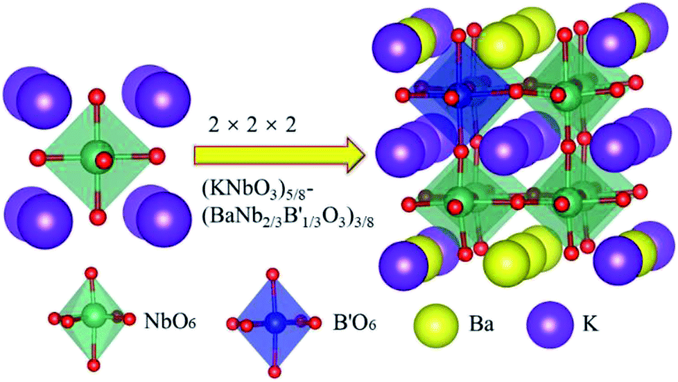 | ||
| Fig. 1 2 × 2 × 2 supercell of (KNbO3)5/8-(BaNb2/3B′1/3O3)3/8 model with 8 cubic perovskite unit cells. In the left unit cell, a centre Nb atom (green) is bonded to six O atoms (red) to form a NbO6 octahedron unit, while K atoms (purple) occupy the corners of the cube. In the right supercell, one dopant atom B′ (blue) replaces one centre Nb atom among eight NbO6 octahedron cages, with Ba atoms (yellow) substituting K atoms at half of the face and edge centred sites on the basal planes of the supercell. | ||
Results and discussion
Geometrical factors
Generally, the tolerance factor and octahedron factor are two key indices for predicting the stability of crystal structures from ionic radius aspect, which can be used as initial indicators in selecting suitable dopants or alloying elements. The tolerance factor (t) is defined by the following formula (1):51
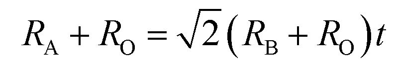 | (1) |
Here Shannon radii are adopted, with K radius being 1.64 Å and Ba 1.61 Å for the A site with 12 coordination, and Nb-0.64 Å and O-1.4 Å for sites with 6 coordination. Ionic radii for transition metals are plotted in Fig. 2. While increased filling of d-orbitals leads to an overall trend of reduced ionic diameter for the 3d transition metals, magnetostriction especially for V, Cr, Mn and Co due to unpaired 3d electrons is behind abnormal deviation from the general trends (Table 1). It is worth pointing out that while DFT with PBE has been widely used for assessment of magnetism, non-local effects in the XC functionals and associated electronic structures would need to be considered for greater accuracy. All 3d elements meet the stability request in the tolerance factor (0.91–1.10) and octahedron factor (0.414–0.732). These two factors show the corresponding trends with radius trend.
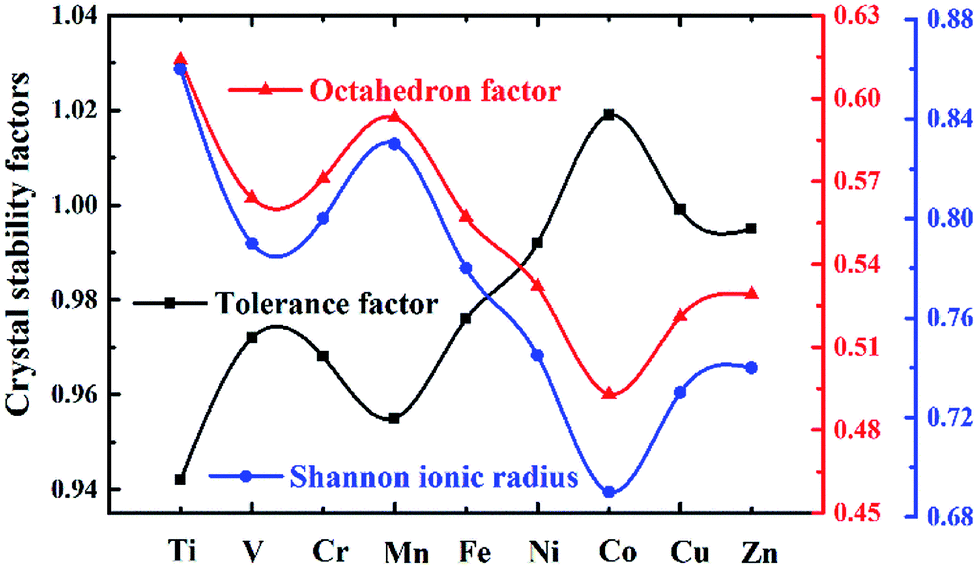 | ||
| Fig. 2 Blue line with dots symbolizes Shannon ionic radius (Å) for 3d TM cations; black line with squares for tolerance factor and red line with triangles for octahedron factor are adopted for crystal stability evaluation. | ||
| Ti | V | Cr | Mn | Fe | Co | Ni | Cu | Zn | |
|---|---|---|---|---|---|---|---|---|---|
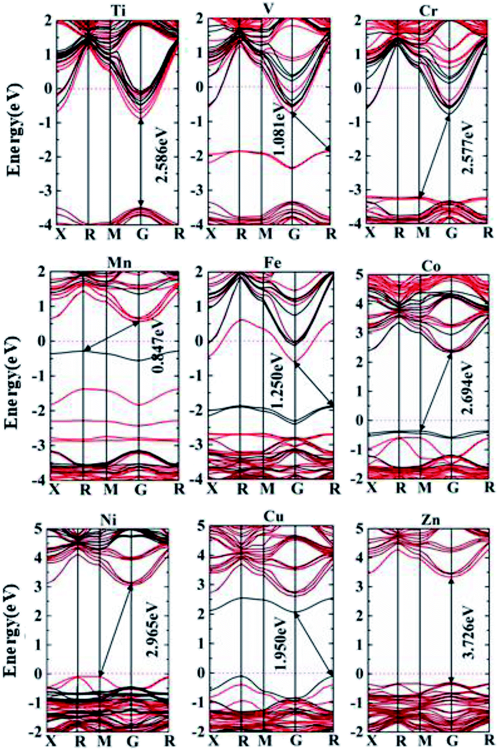
| Eg (eV) | 2.586 | 1.081 | 2.577 | 0.847 | 1.250 | 2.694 | 2.965 | 1.950 | 3.726 |
| Transition path | G → G | R → G | M → G | R → G | R → G | M → G | M → G | R→G | G→G |
| Character | n | n | n | — | n | — | p | p | — |
| Application | TCO | PV | TCO | PV | PV | — | TCO | PV | — |
| Shell | 3d24s2 | 3d34s2 | 3d54s1 | 3d54s2 | 3d64s2 | 3d74s2 | 3d84s2 | 3d104s1 | 3d104s2 |
| Orbit | 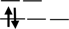 |
 |
 |
 |
 |
 |
 |
 |
 |
| μB (B. M.) | 0.494 | 2.302 | 3.497 | 4.996 | 0.002 | 0.818 | 1.998 | 0.998 | 0 |
Stable structures of doped supercells are obtained by geometric relaxation. The resultant supercell deviates from the cubic structure slightly, with c-axis being slightly larger than a (Table S2†). Overall the resultant supercells expand due to substitution of one eighth of Nb by other 3d elements, which is consistent with B′–O bond length increasing with the atomic number of the dopant, Fig. 3a. This is understandable as the electronegativity of 3d elements generally increases, thus impacting ionic interaction between B′ and O. The abnormality for Mn and Fe doped systems is associated with their rather different magnetic momentums (Table 1), as higher spin polarization causes lattice extension, and vice versa.53 Also, with increasing filling of 3d shell of dopant, the bond angle of O–B′–O chain gradually deviates from standard 180° due to lattice distortion with Mn and Zn showing the maximum 15° offset, as shown in Fig. 3b. The same situation happens in the octahedral tilt angle between NbO6 and B′O6 octahedrons with the increasing distortion, Fig. 3c.
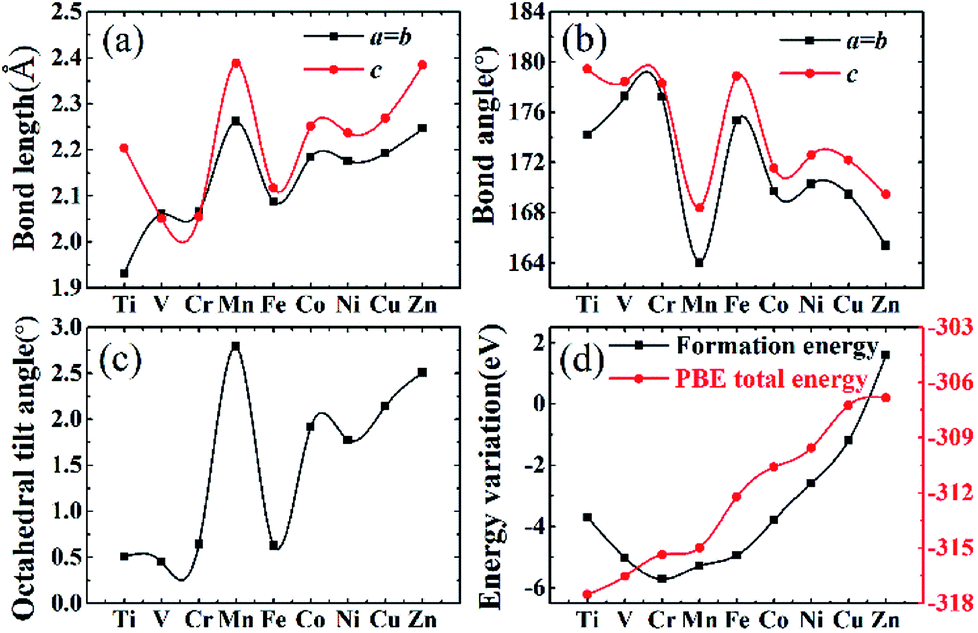 | ||
| Fig. 3 (a) and (b) refer to bond length and bond angle from B′ dopant and the nearest oxygen, black line with blocks for a and b axes variation and red line with dots for c axis. (c) Maximum tilt angle of B′O6 octahedron with respect to a neighbouring NbO6 octahedron. (d) The energy variation including formation energy and total energy. | ||
The calculated formation energy is used to predict the stability of doped systems. The formation energy for B′ substitution of one Nb is termed as:
| Ef = −(Etotal − EKNbO3 − EB′) | (2) |
Lattice parameters for all doped systems are listed in Table S2.† Because Shannon radii of all chosen transition metals are bigger than parent centre atom Nb, so that lattice parameters of doped structures are all larger than undoped KNbO3, with the maximum enlargement by 0.252 Å in Mn doped lattice. The slight tetragonality (c/a) in doped structures is consistent with acceptable geometrical factors for stabilized perovskite structures.
Electronic structures
Firstly, band structure of 2 × 2 × 2 supercells of intrinsic cubic KNbO3 (40 atoms) are calculated using the HSE06 functional to consider non-local effect typically important in metal oxides. The resultant direct band gap of 2.74 eV, Fig. 4a, which is slightly larger than the outcome from previous assessment (2.65 eV).48 Partial densities of states show that O 2p states located at around −0.3 eV define the valence band maximum (VBM), and Nb 3d states at 2.4 eV determine the conduction band minimum (CBM),55 while the states from K do not contribute to the bandgap value due to its being located at deep energy levels, as shown in Fig. 4b. For total DOS of KNbO3, the spin-up states are compensated by spin-down states, leading to zero magnetism.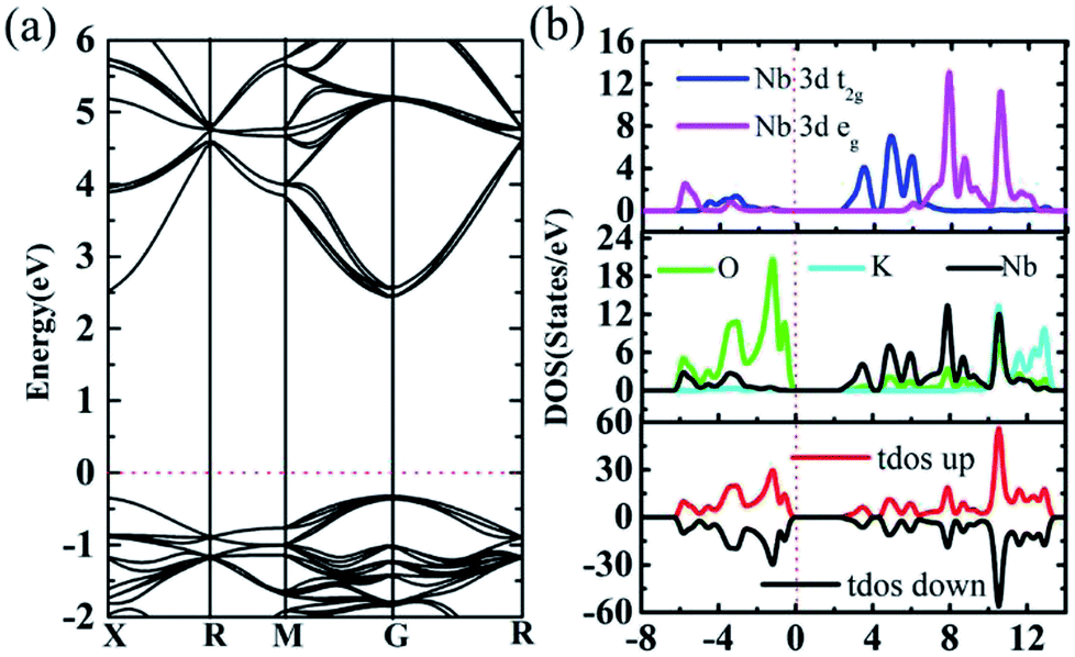 | ||
| Fig. 4 (a) KNbO3 band structure from HSE06 calculation with direct 2.74 eV band gap. (b) KNbO3 total and partial DOS from HSE06 calculation. The high symmetry paths for cubic KNbO3 are X (0.5, 0, 0), R (0.5, 0.5, 0.5), M (0.5, 0.5, 0), G (0, 0, 0) and R (0.5, 0.5, 0.5). | ||
Fig. 5 illustrates three phases for the splitting of degenerate states of the octahedral centre atom under different conditions. Here the degenerate d10 shell configuration (phase I) is taken as an example to explain the following splitting process. Each orbital is occupied by two electrons with opposite spin orientation under the Hund rule and Pauli exclusion principle. Under the impact of crystal field theory, original fivefold degenerate states split into double degenerate states eg (d2z and dx2−y2) with higher energy level and threefold degenerate states t2g (dxy, dyz and dxz) with lower energy level. Normally the stretch direction of t2g orbitals are along the diagonal directions between every two coordinate axes, resulted in t2g orbitals usually possessing lower energy with respect to these of eg orbitals. Interestingly, degenerate eg and t2g states will be further split using a hybrid functional such as HSE06, thus resulting in more independent states contributing to electronic structures, where eg states split into higher dx2−y2 and lower d2z states and t2g states develop into higher dxy and double degenerate dyz and dxz states along the c axis with lower energy. Such an effect is termed as extensive tuning from previous work on the non-degeneration states owing to anion substitution in the octahedron cage.56
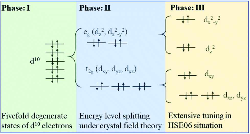 | ||
| Fig. 5 The schematic diagram of TM 3d10 fivefold degenerate states splitting under crystal field and non-local effect in HSE06. | ||
The electronic polarization is considered in the calculation of electronic structures, with bands of different spin characters presented in red and black respectively in the band structures, Fig. 6. Spin-polarized band structures and associated total and partial density of states (Fig. 7) are combined to assess the effect of impurity states on the overall electronic structures:
 | ||
| Fig. 6 Spin-polarized band structures from HSE06 calculation from Ti–Zn doped systems, red and black lines compose of spin-up bands and spin-down bands, respectively. The high symmetry paths for cubic KNbO3 are X (0.5, 0, 0), R (0.5, 0.5, 0.5), M (0.5, 0.5, 0), G (0, 0, 0) and R (0.5, 0.5, 0.5). | ||
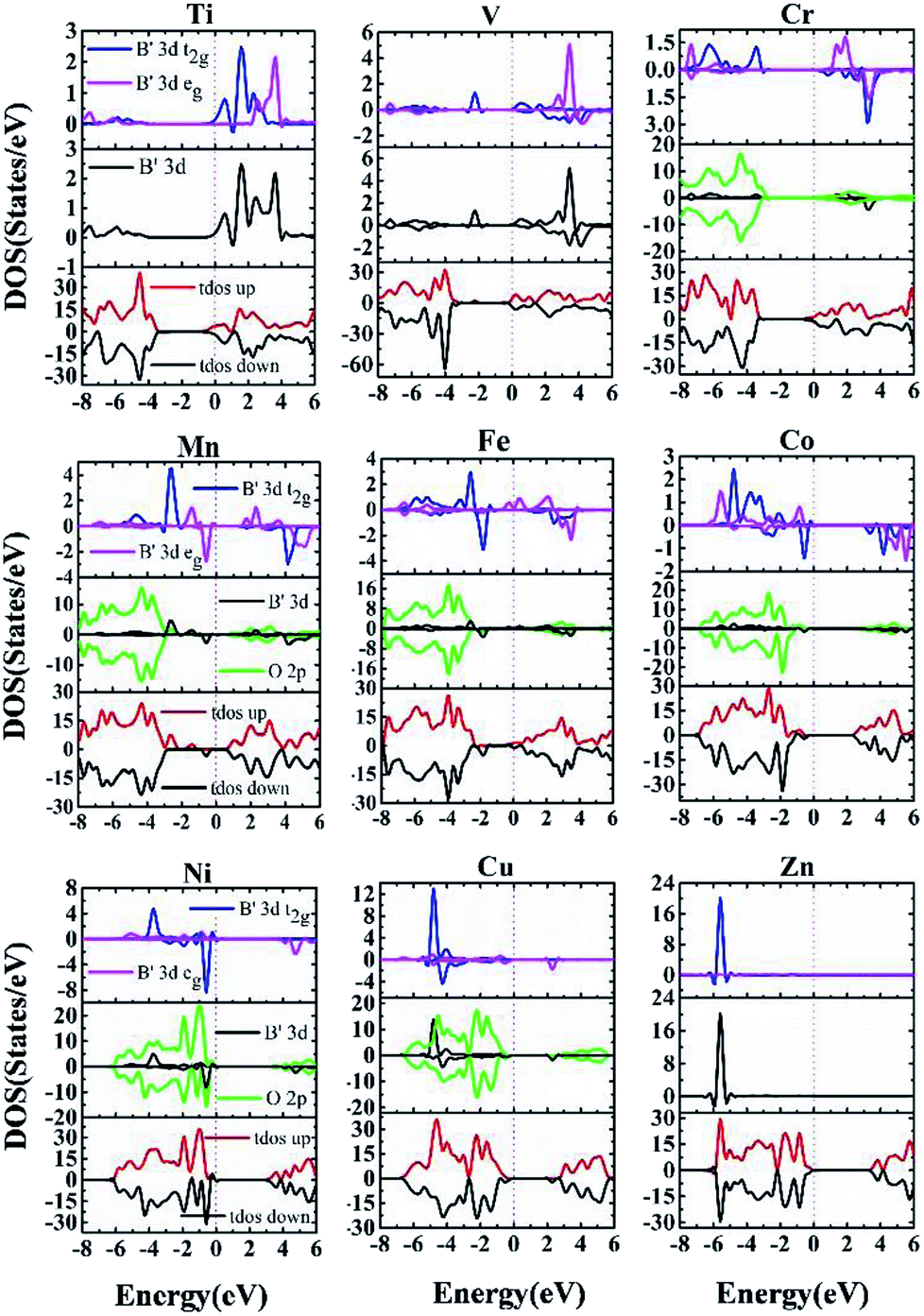 | ||
| Fig. 7 Spin-polarized total and partial DOS from HSE06 calculation from Ti–Zn doped systems. The top chart plots their spin-up and spin-down partial DOS from B′ 3d eg and t2g states; the middle chart for B′ 3d and O 2p total DOS and the last chart for total DOS from the whole system. | ||
In summary, being rather different from doping binary oxides such as TiO2,37–41,57,58 the doping effect of 3d transition metals into perovskite oxides is rather complex, owing to the presence of non-transition metals in the A sites. The overall effects on conducting characteristics and potential applications are presented in Table 1, such that early transition metal doping from Ti to V leads to n-type characteristics. The existence of mid-gap bands such as V-, Mn- and Fe-doped materials are expected to permit multi-wavelength absorption, making them potential candidates for PV or photocatalytic applications. Ni and Cu doping leads to p-type characteristics, making them quite interesting for p-type TCO and optical absorber for solar cells, respectively. Zn and Co doped materials are free of gap states, with intrinsic nature for their VBM being evidently below the Fermi energy like the host phase.
Effective carrier mass and mobility
Carrier mass and associated mobility are important for semiconductors, especially for those suitable either for TCO or effective PV materials. Here we examine their transport properties using a simple approach based on the deformation potential theory,59
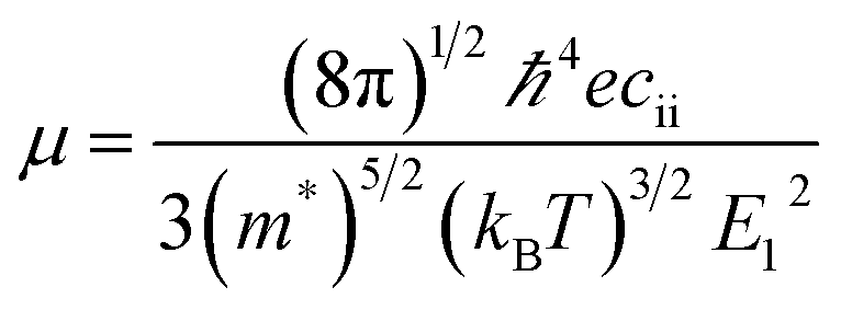 | (3) |
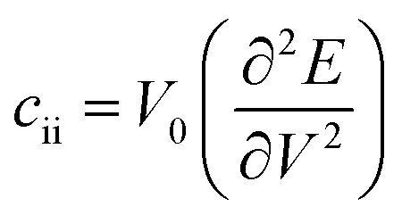 for the elastic constant, V0 is the lattice volume; m* for the carrier effective mass (inversely proportional to the band curvature at CBM or VBM for electrons and holes, respectively); kB for the Boltzmann constant; T for temperature (300 K).
 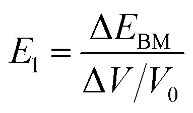 for the deformation potential, the energy shifting of the band edge with respect to the volume variation (ΔV) along the original lattice (V0).
We consider effective electron masses and mobilities for Ti and Cr doped systems for their donor characteristics (n-type), and effective masses of holes are evaluated for Ni and Cu doped systems with acceptor characteristics (p-type) in Table 2. The CBM for Ti or Cr doped materials are located at the G point, which shows remarkable curvature along the (![[1 with combining macron]](https://www.rsc.org/images/entities/char_0031_0304.gif) 0) and (111) directions in the reciprocal space, Fig. 6. Radical shift of CBM down below the Fermi energy is induced owing to replace 1/8 of the Nb species in the 2 × 2 × 2 supercell (40 atoms), making the semiconductor into degenerated metallic phases. This provides a fundamental basis for a large scope of tuning of carrier concentration, by adjusting the percentage of substituted Nb in the material, e.g. from 1% up to 12.5% (1/8). The lower percentages of Nb substitution important to practical doping levels are too big for tractable investigation using hybrid functionals such as the HSE06, e.g. 3.7% Nb substitution already involves 27 unit-cells of perovskite (135 atoms). It is worth mentioning that the overall doping effect at lower doing levels would be similar, except for lower density of states and narrower impurity bands. Such doping concentration effect was studiously demonstrated previously in Mn- or Zn-doped TiO2.38,40
0) and (111) directions in the reciprocal space, Fig. 6. Radical shift of CBM down below the Fermi energy is induced owing to replace 1/8 of the Nb species in the 2 × 2 × 2 supercell (40 atoms), making the semiconductor into degenerated metallic phases. This provides a fundamental basis for a large scope of tuning of carrier concentration, by adjusting the percentage of substituted Nb in the material, e.g. from 1% up to 12.5% (1/8). The lower percentages of Nb substitution important to practical doping levels are too big for tractable investigation using hybrid functionals such as the HSE06, e.g. 3.7% Nb substitution already involves 27 unit-cells of perovskite (135 atoms). It is worth mentioning that the overall doping effect at lower doing levels would be similar, except for lower density of states and narrower impurity bands. Such doping concentration effect was studiously demonstrated previously in Mn- or Zn-doped TiO2.38,40
| Ti (n) | Cr (n) | Ni (p) | Cu (p) | |||||||
|---|---|---|---|---|---|---|---|---|---|---|
| (0) |
(111) | (0) |
(111) | (011) | (0) |
(111) | (011) | (00) |
(111) | |
| m*/m0 | 0.02 | 0.03 | 0.02 | 0.03 | 0.24 | 0.03 | 0.17 | 0.11 | 0.05 | 0.03 |
| μ | 613.58 | 273.93 | 488.27 | 242.56 | 1.09 | 210.33 | 2.39 | 6.81 | 71.77 | 257.29 |
The effective electron masses are about the same in Cr or Ti doped materials, being 0.02 along the (0) direction and 0.03 along (111), in the reciprocal space. This leads to very high electron mobility, such that for Ti doped perovskite, the mobility in the (0) direction is over 4000 times of that in Si (1500 cm2 V−1 s−1). The direct band nature of the material provides great leverage for its use as a n-type semiconductor in diodes for various applications, when doping level is low. At heavier doping level, the material is to be highly attractive as a TCO based on sustainable materials resources, so that resource crisis due to the depletion of indium metal for ITO can be addressed with a promising alternative. For the Ni and Cu doped materials, one notes that evident lifting of the VBM with reference to the case of the host material, indicating tendency for p type characteristics. Ni doping leads to VBM to appear at the M point (0.5, 0.5, 0), with curvature towards the G point direction being much more pronounced than that towards the R point (0.5, 0.5, 0.5). The corresponding directions in the reciprocal space are (011), (0) and (111), respectively. The maximum hole mobility in the (0) direction is also over 4600 times of that in silicon. For Cu doped material, the VBM is at the R point (0.5, 0.5, 0.5). In this case, the curvatures towards both the X (0.5, 0, 0) and M (0.5, 0.5, 0) points are very high, corresponding to the directions of (011) and (00). Again, the maximum hole mobility along (111) is thousands of times bigger than that in silicon. Therefore, the Ni doped material would be expected to be a superb p-type TCO yet missing, and the Cu doped material with remarkably reduced band gap would be a potential candidate for effective photovoltaic applications.
Comparing to reported data, the carrier mobilities over ∼106 cm2 V−1 s−1 is in the same order of theoretically predicted data in superb two-dimensional materials.60 They are significantly higher than reported experimental data in hybrid perovskites. For example, measured hole mobility in CH3NH3PbI3 was 164 ± 25 cm2 V−1 s−1 and the experimentally measured electron mobility in (Ba, La)SnO3 (TCO) was 320 cm2 V−1 s−1.61,62 The theoretically reported carrier mobilities for electrons and holes in CH3NH3PbI3 are 7000–30![[thin space (1/6-em)]](https://www.rsc.org/images/entities/char_2009.gif) 000 cm2 V−1 s−1 and 1500–5500 cm2 V−1 s−1 respectively.63 It is generally observed that theoretically predicted carrier mobilities could be significantly bigger than experimentally reported values, due to existence of various structural defects in real materials.
000 cm2 V−1 s−1 and 1500–5500 cm2 V−1 s−1 respectively.63 It is generally observed that theoretically predicted carrier mobilities could be significantly bigger than experimentally reported values, due to existence of various structural defects in real materials.
Conclusion
First-principle modelling in the framework of the density functional theory has been carried out to study the effect of 3d transition metal (B′) doping to perovskite materials based on KNbO3, i.e. (KNbO3)5/8-(BaNb2/3B′1/3O3)3/8.Unlike in binary oxides such as TiO2, the doping effect into perovskite is rather complex. In the simplest case such as doping with earlier transition metals Ti and Cr, the CBM is shifted effectively downwards with electron mobilities thousands of times higher than that in silicon. This makes them remarkable candidates for TCO alternatives using sustainable resources.
The middle transition metals such as Mn and Fe tend to bring about intermediate bands within the forbidden gap. Unpaired valence electrons with associated spin polarization promotes non-degenerated orbital occupation, which in turn helps formation of gap states, so that intermediate bands appear in V, Mn and Co doped materials. The presence of curvy intermediate bands within the forbidden gap would enhance optical absorption, as multi-wavelength absorption is enabled owing to optically relaying effect. This opens potential use of the materials for photovoltaic or photocatalytic applications.
Later transition metal Ni and the noble metal Cu bring about p-type characteristics together with very large hole mobility. Ni doping is of great potential as a p-type TCO yet missing in the semiconductor family, and Cu doped materials is considered to be a potential material for high performance solar cells.
Conflicts of interest
There are no conflicts to declare.Acknowledgements
This work was funded in part by Zhengzhou Materials Genome Institute, the National Natural Science Foundation of China (No. 51001091, 111174256, 91233101, 51602094, and 11274100), and the Fundamental Research Program from the Ministry of Science and Technology of China (No. 2014CB931704). YL thanks Dr Zhuo Wang for technical training and helpful discussions.Notes and references
- W. Shockley and H. Queisser, J. Appl. Phys., 1961, 32, 510 CrossRef CAS.
- M. A. Green, Prog. Photovolt: Res. Appl., 2009, 17, 183–189 CrossRef CAS.
- A. Kojima, K. Teshima, Y. Shirai and T. Miyasaka, J. Am. Chem. Soc., 2009, 131, 6050–6051 CrossRef CAS PubMed.
- A. B. Yusoff, P. Gao and M. K. Nazeeruddin, Coord. Chem. Rev., 2018, 373, 258–294 CrossRef.
- A. Abate, Joule, 2017, 1, 659–664 CrossRef CAS.
- M. R. Filip, S. Hillman, A. A. Haghighirad, H. J. Snaith and F. Giustino, J. Phys. Chem. Lett., 2016, 7, 1254–1259 CrossRef PubMed.
- X. G. Zhao, D. W. Yang, J. C. Ren, Y. H. Sun, Z. W. Xiao and L. J. Zhang, Joule, 2018, 2, 1–12 CrossRef.
- H. J. Zhang, G. Chen, X. D. He and J. Xu, J. Alloys Compd., 2012, 516, 91–95 CrossRef CAS.
- H. J. Zhang, G. Chen, Y. X. Li and Y. J. Teng, Int. J. Hydrogen Energy, 2010, 35, 2713–2716 CrossRef CAS.
- R. B. Comes, P. V. Sushko, S. M. Heald, R. J. Colby, M. E. Bowden and S. A. Chambers, Chem. Mater., 2014, 26, 7073–7082 CrossRef CAS.
- T. Onishi, Top. Catal., 2010, 53, 566–570 CrossRef CAS.
- F. Yang, L. Yang, C. Z. Ai, P. C. Xie, S. W. Lin, C. Z. Wang and X. H. Lu, Nanomaterials, 2018, 8, 455 CrossRef PubMed.
- Z. Teng, J. J. Jiang, G. Y. Chen, C. L. Ma and F. W. Zhang, AIP Adv., 2018, 8, 095216 CrossRef.
- I. Masuda, K. I. Kakimoto and H. Ohsato, J. Electroceram., 2004, 13, 555–559 CrossRef CAS.
- J. A. Astudillo, S. A. Dionizio, J. L. Izquierdo, O. Moŕan, J. Heiras and G. Bolãnos, AIP Adv., 2018, 8, 055817 CrossRef.
- W. Cai, C. L. Fu, R. L. Gao, W. H. Jiang, X. L. Deng and G. Chen, J. Alloys Compd., 2014, 617, 240–246 CrossRef CAS.
- T. Choi, S. Lee, Y. J. Choi, V. Kiryukhin and S. W. Cheong, Science, 2009, 324, 63 CrossRef CAS PubMed.
- M. L. Cohen, Science, 1993, 261, 307–308 CrossRef CAS PubMed.
- I. Grinberg, D. V. West, M. Torres, G. Y. Gou, D. M. Stein, L. Y. Wu, G. N. Chen, E. M. Gallo, A. R. Akbashev and P. K. Davies, Nature, 2013, 503, 509–512 CrossRef CAS PubMed.
- W. L. Zhou, H. M. Deng, P. X. Yang and J. H. Chu, Appl. Phys. Lett., 2014, 105, 111904 CrossRef.
- W. L. Zhou, H. M. Deng, L. Yu, P. X. Yang and J. H. Chu, J. Phys. D: Appl. Phys., 2015, 48, 455308 CrossRef.
- W. L. Zhou, H. M. Deng, L. Yu, P. X. Yang and J. H. Chu, Mater. Lett., 2017, 202, 39–43 CrossRef.
- L. M. Yu, J. H. Jia, G. W. Yi, Y. Shan and M. M. Han, Mater. Lett., 2016, 184, 166–168 CrossRef CAS.
- S. F. Si, H. M. Deng, W. L. Zhou, T. T. Wang, P. X. Yang and J. H. Chu, Ceram. Int., 2018, 44, 14638–14644 CrossRef CAS.
- Q. F. Zhang, F. Xu, M. J. Xu, L. Li, Y. M. Lu, M. K. Li, P. Li, M. Li, G. Chang and Y. B. He, Mater. Res. Bull., 2017, 95, 56–60 CrossRef CAS.
- R. P. Tiwari, J. Shah, R. K. Kotnala and B. Birajdar, J. Alloys Compd., 2018, 753, 642–645 CrossRef CAS.
- B. Q. Song, X. J. Wang, C. Xin, L. L. Zhang, B. Song, Y. Zhang, Y. Wang, J. Wang, Z. G. Liu, Y. Sui and J. K. Tang, J. Alloys Compd., 2017, 703, 67–72 CrossRef CAS.
- F. G. Wang, I. Grinberg and A. M. Rappe, Phys. Rev. B: Condens. Matter Mater. Phys., 2014, 89, 235105 CrossRef.
- C. Lohaus, C. Steinert, G. Deyu, J. Brötz, W. Jaegermann and A. Klein, Appl. Phys. Lett., 2018, 112, 152105 CrossRef.
- I. Hamberg and C. G. Granqvist, J. Appl. Phys., 1986, 60, R123–R160 CrossRef CAS.
- G. G. Untila, T. N. Kost and A. B. Chebotareva, Sol. Energy, 2018, 159, 173–185 CrossRef CAS.
- S. Y. Liu, S. Liu, Y. Y. Zhou, Y. J. Piao, G. J. Li and Q. Wang, Appl. Phys. Lett., 2018, 113, 032102 CrossRef.
- L. Lu, M. L. Guo, S. Thornley, X. Han, J. H. Hu, M. J. Thwaites and G. S. Shao, Sol. Energy Mater. Sol. Cells, 2016, 149, 310–319 CrossRef CAS.
- B. H. Wang, W. Zhang, K. B. Yang, T. Liao, F. Z. Li, Y. Y. Cui, Y. F. Gao and B. Liu, Ceram. Int., 2018, 44, 16051–16057 CrossRef CAS.
- M. A. Riza, M. A. Ibrahim, U. C. Ahamefula, M. A. Mat Teridi, N. A. Ludin, S. Sepeai and K. Sopian, Sol. Energy, 2016, 137, 371–378 CrossRef CAS.
- G. Kresse and J. Furthmller, Comput. Mater. Sci., 1996, 6, 15–50 CrossRef CAS.
- G. Shao, J. Phys. Chem. C, 2009, 113, 6800–6808 CrossRef CAS.
- G. Shao, J. Phys. Chem. C, 2008, 112, 18677 CrossRef CAS.
- X. P. Han, K. Song, L. Liu, Q. Deng, X. Xia and G. Shao, J. Mater. Chem. C, 2013, 1, 3736 RSC.
- X. P. Han and G. Shao, Phys. Chem. Chem. Phys., 2013, 15, 9581 RSC.
- X. P. Han and G. Shao, J. Mater. Chem. C, 2011, 115, 8274 CAS.
- P. E. Blochl, Phys. Rev. B: Condens. Matter Mater. Phys., 1994, 50, 953–979 CrossRef.
- J. P. Perdew, K. Burke and M. Ernzerhof, Phys. Rev. Lett., 1996, 77, 3865–3868 CrossRef CAS PubMed.
- J. Heyd, G. E. Scuseria and M. Ernzerhof, J. Chem. Phys., 2003, 118, 8207–8215 CrossRef CAS.
- J. Heyd, G. E. Scuseria and M. Ernzerhof, J. Chem. Phys., 2006, 124, 219906 CrossRef.
- J. Paier, M. Marsman, K. Hummer, G. Kresse, I. C. Gerber and J. G. Angyan, J. Chem. Phys., 2006, 124, 154709 CrossRef CAS PubMed.
- M. Marsman, J. Paier, A. Stroppa and G. Kresse, J. Phys.: Condens. Matter, 2008, 20, 064201 CrossRef CAS PubMed.
- F. Wang and A. M. Rappe, Phys. Rev. B: Condens. Matter Mater. Phys., 2015, 91, 165124 CrossRef.
- C. L. Diao and H. W. Zheng, J. Mater. Sci.: Mater. Electron., 2015, 26, 3108–3111 CrossRef CAS.
- G. Kresse, M. Marsman, and J. Furthmuller, VASP the GUIDE, 2009, pp. 61–135 Search PubMed.
- Z. Li, M. J. Yang, J. S. Park, S. H. Wei, J. J. Berry and K. Zhu, Chem. Mater., 2016, 28, 284–292 CrossRef CAS.
- Z. W. Xiao and Y. F. Yan, Adv. Energy Mater., 2017, 7, 1701136 CrossRef.
- R. Q. Wu, J. Appl. Phys., 2002, 91, 7358 CrossRef CAS.
- W. Y. Yu, Z. L. Zhu, C. Y. Niu, C. Li, J. H. Cho and Y. Jia, Nanoscale Res. Lett., 2016, 11, 77 CrossRef PubMed.
- T. Neumann, G. Borstel, C. Scharfschwerdt and M. Neumann, Phys. Rev. B: Condens. Matter Mater. Phys., 1992, 46, 10623–10628 CrossRef CAS.
- H. Kageyama, K. Hayashi, K. Maeda, J. P. Attfield, Z. Hiroi, J. M. Rondinelli and K. R. Poeppelmeier, Nat. Commun., 2018, 9, 772 CrossRef PubMed.
- K. N. Song, X. P. Han and G. Shao, J. Alloys Compd., 2013, 551, 118–124 CrossRef CAS.
- Q. R. Deng, X. P. Han, Y. Gao and G. Shao, J. Appl. Phys., 2012, 112, 013523 CrossRef.
- J. Bardeen and W. Shockley, Phys. Rev., 1950, 80, 72–80 CrossRef CAS.
- E. H. Hwang and S. D. Sarma, Phys. Rev. B: Condens. Matter Mater. Phys., 2007, 11, 77 Search PubMed.
- Q. F. Dong, Y. J. Fang, Y. C. Shao, P. Mulligan, J. Qiu, L. Cao and J. S. Huang, Science, 2015, 347, 967–970 CrossRef CAS PubMed.
- H. J. Kim, U. Kim, T. H. Kim, J. Kim, H. M. Kim, B. G. Jeon, W. J. Lee, H. S. Mun, K. T. Hong and J. Yu, Phys. Rev. B: Condens. Matter Mater. Phys., 2012, 86, 16 Search PubMed.
- Y. W. Wang, Y. B. Zhang, P. H. Zhang and W. Q. Zhang, Phys. Chem. Chem. Phys., 2015, 17, 11516–11520 RSC.
Footnote |
| † Electronic supplementary information (ESI) available. See DOI: 10.1039/c9ra00289h |
| This journal is © The Royal Society of Chemistry 2019 |