
 Open Access Article
 This Open Access Article is licensed under a Creative Commons Attribution-Non Commercial 3.0 Unported Licence
Motion sensors achieved from a conducting polymer-metal Schottky contact†
Yang Zhou,
Jian Fang,
Hongxia Wang,
Hua Zhou,
Guilong Yan,
Hao Shao,
Yan Zhao and
Tong Lin *
*
Institute for Frontier Materials, Deakin University, Geelong, Victoria 3216, Australia. E-mail: tong.lin@deakin.edu.au
First published on 25th February 2019
Abstract
Mechanical-to-electrical energy conversion devices show potential applications in the detection of movements. Previous studies on these sensor devices are mainly based on piezoelectricity or triboelectricity, which typically generates AC signals. In this study, a movement sensor that generated DC signals based on a conducting polymer-metal Schottky diode was prepared for the first time. Using the Al|poly(3,4-ethylenedioxythiophene)|Au device as a model, we showed that the sensor device could detect the touch and sliding movements. Both the pressure of the Al electrode touching the PEDOT surface and its sliding speed affected the voltage outputs. The device showed a high response speed of 1.7 s at 39.8 kPa. The modified device can even measure the sliding speed. The DC output allows the use of electrical energy for running other electronic devices. A conducting polymer-metal Schottky contact may be useful for the development of DC output movement sensors.
Introduction
Motion detection has wide applications in the fields of robotics,1,2 automobiles,3–5 sports,6–8 health/ageing care,9 human-machine communication and manufacturing industry.10 Motion detection sensors can be prepared based on a variety of principles, including optics, acoustics, microwave, resistivity and capacitance, depending on the application purpose. For example, a passive IR sensor is able to detect people's movement according to the mid-infrared radiation emitted from the human body.11 Microwave sensors (also known as Doppler radar) can detect outdoor human activities such as walking and running.12 Resistive or capacitive sensors (e.g., touchscreens) are broadly used in computers, smartphones and other digital devices where a command is issued simply by pressing or sliding the fingers on the screen.13,14Over recent years, the rapid development in microelectronics and wireless communication has increased the demand for movement detection.15–17 Thus, highly sensitive, multifunctional motion detectors are highly desirable. Capacitive touchscreens utilize the human body as an electrical conductor to distort the electrostatic field on the screen and alter the capacitance.18–20 However, they fail to detect the insulating materials. Resistive sensors suffer from low contrast and insufficient sensitivity. Moreover, the structural complexity and high cost cause problems in their large scale production.
Recently, energy harvesters capable of converting mechanical energy into electricity have shown significant potential for motion detection applications.21,22 Movement and pressure sensors based on a triboelectric nanogenerator (TENG) and a piezoelectric nanogenerator (PENG) have been reported. TENGs generate triboelectric charges when two materials with opposite electric negative features contact and separate.23 Fan et al.24 prepared a pressure sensor using polydimethylsiloxane (PDMS) and polyester as active materials. The device was able to detect the impact from dropping water (3.6 Pa) or a falling feather (0.4 Pa) on the surface, with a low-end detection limit of ∼13 mPa. Zhu et al.25 reported a polymer nanowire TENG sensor, which showed a pressing sensitivity of up to 44 mV Pa−1 and touch sensitivity of 1.1 V Pa−1. Yang et al.9 prepared self-powered movement sensors using a single-electrode TENG mechanism, which required the moving objects to be connected with an electrode. PENGs can convert mechanical energy, vibration and hydraulic energy into electrical signals useful for the development of wearable sensors.26 Chun et al.21 prepared a self-powered sensor for the detection of motion. The sensor device consisted of piezoelectric hemispheres embedded in PDMS. It generated an output of 4.0 V and 0.13 μA cm−2. The device can sense wrist movement in various directions. Proto et al.27 compared two piezoelectric transducers, i.e., lead zirconate titanate (PZT) and polyvinylidene fluoride (PVDF), for sensing body movement. The power output generated by a single transducer in common activities was in the range of 2–46 μW cm−3, and the output signals could be further amplified using a group of devices. Wang et al.28 reported a biocompatible body movement sensor with a combination of PENG and TENG using aluminium/zinc oxide as a transparent electrode, polyvinylidene fluoride trifluoroethylene as a piezoelectric layer, and PDMS as a friction layer. This TENG–PENG hybrid device can distinguish slight body movements of the neck, finger, elbow, and ankle. However, both TENG and PENG require repeated attachment and detachment of the two active materials, and they have complex device structures.29 These issues not only narrow the application scope but also increase the fabrication difficulty. In addition, the TENG and PENG devices typically generate alternating current (AC) voltage signals, which need rectification into direct current (DC) when used for power supplying purposes (e.g. self-powered sensors). In this regard, DC sensors are promising towards self-powered applications. However, DC movement sensors based on the mechanical to electrical energy conversion principle have not been reported in the literature.
In previous studies, we have prepared a conducting polymer-metal Schottky contact energy harvester that can convert mechanical energy into DC electric signals without rectification.30 Under compressive deformation, the device can generate a DC power of 0.7 V and 62.4 μA cm−2. The devices could be used either as power suppliers or as sensors.
In this study, we report a novel movement sensor based on a conducting polymer-metal Schottky contact. Poly(3,4-ethylenedioxythiophene) (PEDOT) and aluminium were used as material models. Motion can be detected when the PEDOT-Al contact was established. The effect of Al-PEDOT mechanical interactions on electric output was examined. We showed that the PEDOT-Al Schottky contact was responsive to the touch and sliding movements. The device can sense low pressure (i.e., 4.0 kPa) and slow movement (e.g. 1.8 cm s−1). The output signals were linearly correlated to the movement speed and load. By dividing the PEDOT surface into separate segments, the device can even measure the movement speed.
Experimental
Materials
3,4-Ethylenedioxythiophene (EDOT), lithium perchlorate (LiClO4) and propylene carbonate (PC) were purchased from Sigma-Aldrich and used as received. Aluminum foils, pencils, an Al rod and a PET film were purchased from a local store. Au was deposited on one side of the PET film using the Leica EM ACE600 sputter coater.Device fabrication
The Au-coated PET film was used as a substrate. PEDOT was electrodeposited on the gold surface using a three-electrode electrochemical system (CHI760D electrochemical workstation), in which a platinum plate (2 cm × 2 cm) and the Ag/AgCl standard electrode were used as the counter and reference electrodes, respectively. The deposition was carried out in a PC solution containing 0.1 M LiClO4 and 1 M EDOT. The electrodeposition potential was set at 1.3 V for 120 s. The resulting film was rinsed three times with deionized water and dried overnight at 60 °C.Characterizations
Surface morphology was observed via scanning electron microscopy (SEM, Zeiss Supra 55VP). Surface roughness was characterized using the Bruker Multimode 8 atomic force microscope (AFM). Fourier transform infrared spectroscopy (FTIR) was conducted using the Bruker Vertex 70 FTIR spectrometer in the attenuated total reflection mode (ATR).Results and discussion
Device preparation
Fig. 1(a) illustrates the sensor setup. A PET film sputter-coated with a thin layer of Au (thickness ∼70 nm) was used as a substrate. A layer of PEDOT was deposited on the Au surface using an electrochemical method. An aluminum rod with a smooth edge tip (effective diameter: 4.0 mm) was used as a metal probe, which was mounted onto a programmable positioning system. When the Al rod was attached to the PEDOT surface, a Schottky contact was formed. The deformation of the PEDTO layer with the Al rod led to the generation of electrical signals.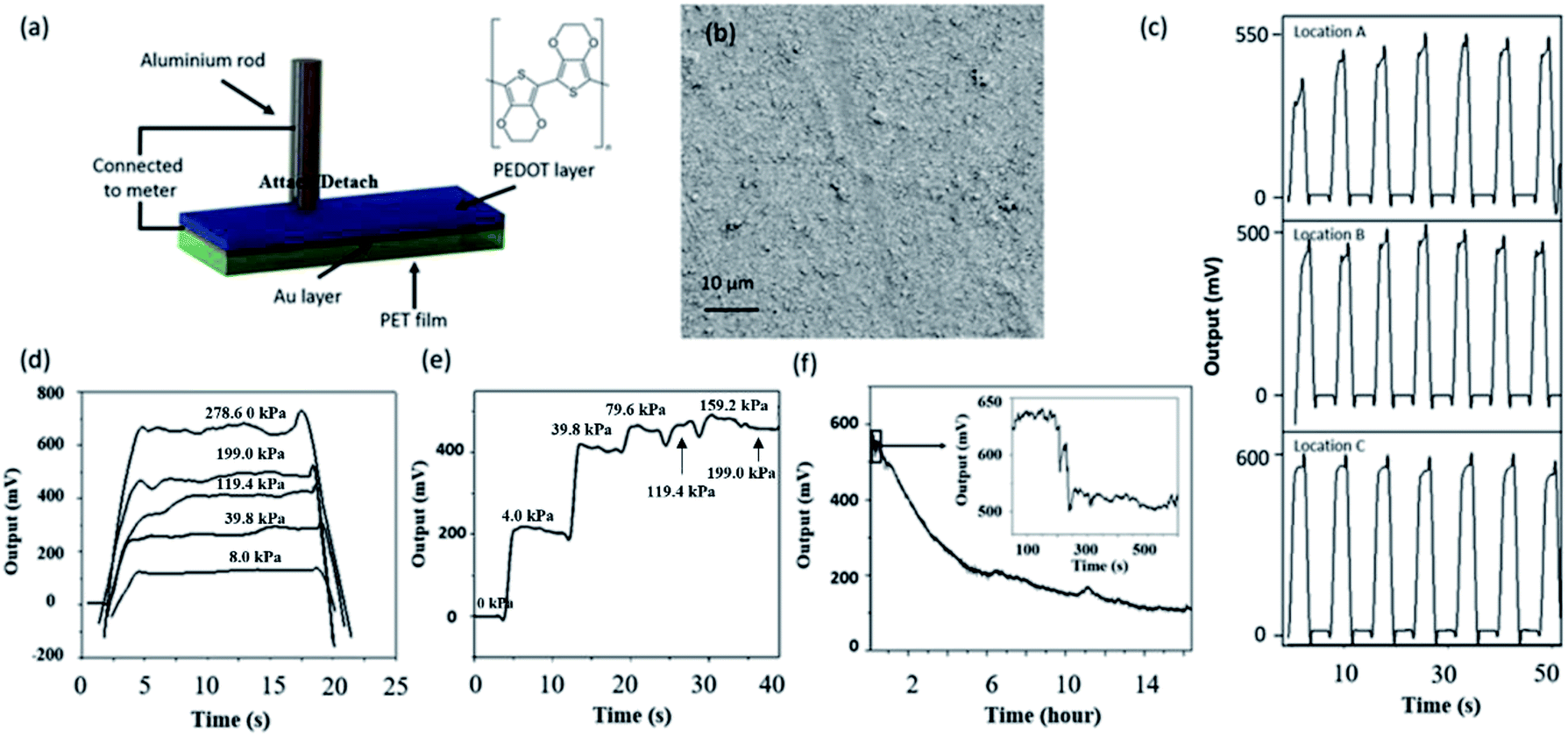 | ||
| Fig. 1 (a) Schematic of the device setup and the chemical structure of PEDOT, (b) an SEM image of the PEDOT surface morphology, (c) output curves of Al rod repeatedly attaching and detaching at three different locations of the PEDOT film, (d) output curves when Al rod attached to and detached from the PEDOT surface at different pressures at the same location, (e) voltage change while pressing the PEDOT film at different pressures, and (f) long time output profile when Al rod was constantly connected to PEDOT (at the same location). | ||
During the electrochemical preparation, the thickness of the PEDOT layer can be adjusted by changing the deposition conditions. However, the PEDOT thickness affected the device stability. When the PEDOT layer was thicker than 5 μm, it had small adhesion strength and tended to delaminate off the PET substrate during contact with the Al rod. On the other hand, when the PEDOT layer was very thin, e.g. thickness < 0.5 μm, it caused uneven coverage on the Au layer; this led to a short circuit when the Al rod was attached to the film (see Fig. S4 in ESI†). In this study, we chose the thickness of 2 μm for the experiments.
The PEDOT film appeared smooth on the surface. However, under SEM, it showed a rough surface structure (Fig. 1(b)). AFM imaging was used to measure the surface roughness. The as-prepared PEDOT film had a root mean square (RMS) roughness of 316 nm.
Conversion of mechanical energy into electricity
Before testing the sensing properties, the energy conversion performance of the Al-PEDOT contact was characterized. Starting with disconnection, the device provided no electric signal (i.e. V = 0). Once the Al rod was attached to the PEDOT surface, a voltage output appeared. Fig. 1(c) illustrates the voltage outputs generated by attaching the Al rod at 1 N pressure force (pressure 79.6 kPa). At three different locations of the PEPOT film, the output showed slightly different values. This can be attributed to the effect of the contact location on the internal resistance. When the connection was at different locations, the device had different system resistances.Fig. 1(d) depicts the typical outputs generated by a short time connection of Al and PEDOT at different pressures. At the same location, the Al-PEDOT connection led to a rapid increase in voltage. In less than 2 seconds, the output value reached a plateau when PEDOT received a pressure in the range of 4.0–199.0 kPa, suggesting a reasonably high response speed. When the Al rod detached from the PEDOT surface, the output sharply turned zero. The pressure applied to the PEDOT surface through the Al tip affected the output value. Higher output values were generated from higher attachment pressure. This trend can be explained by the fact that higher pressure results in larger deformation on PEDOT that leads to larger strain.9 As expected, the device output during the attachment and detachment process was in single polarity, showing a DC voltage characteristic. This DC output feature is similar to that of the layered film Al|PEDOT|Au devices reported in our previous study.31
To verify the Schottky contact, we obtained the I–V curve of the Al|PEDOT|Au setup. Indeed, the Schottky diode feature formed in the device (see Fig. S1 in ESI†).
Fig. 1(e) shows the influence of pressure on the output value when the Al rod was attached to the PEDOT film. Initially, when the Al tip was gently attached to the PEDOT surface at a pressure of 4.0 kPa, the output was maintained at 200 mV with a slight decay in the value. When larger pressure, e.g. 39.8 kPa, was loaded on the Al tip, the voltage rapidly increased to 400 mV and then stabilized at 400 mV. A further increase in the pressure from 39.8 to 79.6 kPa led to a smaller increase in the output value. However, when the pressure was above 79.6 kPa, the output voltage was less sensitive to pressure. This was presumably because the deformation level of the underlying PEDOT film reached its limit. This trend is different from that in the attachment-detachment mode. Since the attachment of Al on PEDOT involves an impact at a certain speed, and extra kinetic energy causes a larger impact deformation in the initial stage.
Fig. 1(f) shows the output profile when the Al rod is attached to the PEDOT surface for a long time. During 16 hours of constant connection, the output voltage decayed from initial 600 mV to 100 mV. The inset chart in Fig. 1(e) shows an enlarged view of the output signal in the first 600 seconds. A stable output was observed before 200 seconds, followed by a slump in the output value. For practical detection, 200 seconds of stable output is adequate for signal collection.
Detection of the movement
To prove the ability to sense a moving object, we moved the Al rod on the PEDOT surface. In one of the experiments, the Al rod was initially disconnected from the PEDOT film, and then, it was attached to the film at a constant speed. Once the tip touched the PEDOT film, voltage signals were detected. In this case, the output signal fluctuated with time. Fig. 2(a) depicts the typical output profile for the sliding tests in the same area, but at different sliding speeds. Sliding at higher speeds resulted in higher output values and vice versa. The response was fast, where the device started to generate stable output signals within 1.7 second when 39.8 kPa pressure was applied. The fluctuation of the output signals suggests variable pressure on the PEDOT layer that leads to a dynamic change in strain. The increase in the output voltage could also originate from the temporarily increased contact area between Al and PEDOT surface.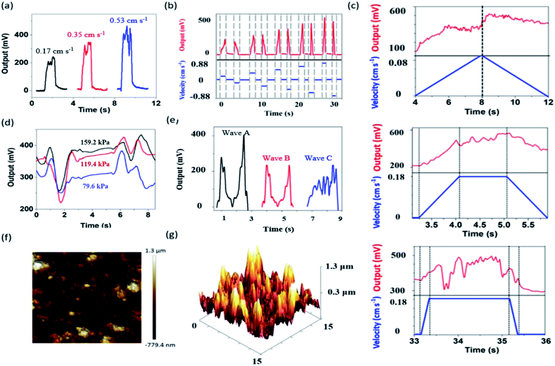 | ||
| Fig. 2 (a) Typical signals generated by sliding, (b)–(d) electric outputs (b) at different movement speeds, (c) with different acceleration modes, and (d) at different pressure levels (sliding speed at 0.18 cm s−1), (e) repeatability of the output signals generated at same location and different locations, (f) 2D and (g) 3D AFM images of the PEDOT films. | ||
Fig. 2(b) shows the output signals generated when the Al rod moved back and forth within the same location at a certain speed, which ranged from 0.18 to 0.88 cm s−1. The negative speed indicated that the movement was in the opposite direction. Since the acceleration and deceleration took less than 0.01 second, the acceleration and deceleration times were neglected. The output signals generated quasi-linearly increased with the increasing speed. Apart from the correlation between the speed and the output signals, the shapes of the two output signals generated within the same location and speed but in the opposite directions were almost symmetric. Due to the identical pressure and movement speed, this similarity was attributable to the similar PEDOT deformation.
We also found that the application of a large pressure during sliding could lead to a damage of the PEDOT layer. When the pressure was in the range of 79.6–159.2 kPa, the sliding did not cause an apparent damage to PEDOT, and the test was repeatable. Under a pressure of 159.2 kPa and an Al movement speed less than 1 cm s−1, the device showed reasonable repeatability.
Fig. 2(c) shows the output results generated by the movement of the Al rod at different acceleration modes. During testing, the Al rod was moved at 0.02, 0.18, and 0.53 cm s−2 along the PEDOT surface (i.e. top, middle and bottom plots, respectively) within the same distance. The maximum speed was controlled at 0.18 cm s−1. When the Al tip moved at the accelerated speed of 0.02 cm s−2 and then decelerated at an opposite accelerated speed, i.e. −0.02 cm s−2, the output voltage increased with an increase in the speed and then reduced correspondingly. However, the maximum output occurred just after the maximum speed value. This voltage hysteresis was caused by the variation of strain. The acceleration phase gradually increased the strain and the deformation force, whereas the deceleration phase reduced these forces. As a result, a combined effect on the voltage output occurred. During the constant speed period, the output signals continued to fluctuate during the movement presumably because of the variation in the PEDOT deformation level and strain. In this circumstance, the movement of the Al rod was considered to be the same as that presented in Fig. 2(b), where high acceleration and deceleration speeds were applied. When the acceleration speed was increased to 0.53 cm s−2, a similar trend was observed.
Note that the output signals in the deceleration state showed a decreased trend; however, the output values were slightly higher when compared with those in the acceleration stage (Fig. 2(c)). This is attributed to the output feature of the Au|PEDOT|Al device. When the device is kept in the deformed state, the voltage output slowly decays (see Fig. 1(e)). In the acceleration stage, the deformed area was just deformed since the contact with the Al tip contributed more to the voltage outputs.
Fig. 2(d) shows the effect of pressure on the output profile when the Al tip moved along the PEDOT surface at 0.18 cm s−1. When the tip pressure was increased, higher output value was obtained, whereas the output profile had a very small change. Therefore, this Schottky device is responsive to both the touch and the sliding movements. Fig. 2(e) shows a comparison of three waves, in which the waves A & B were generated from repeated sliding in the same location, whereas the wave C was generated at different locations of the same PEDOT film. Herein, the Pearson's correlation coefficient between two input data series was employed to characterize the output waves. The Person correlation coefficient was calculated by the eqn (1):
 | (1) |
![[x with combining macron]](https://www.rsc.org/images/entities/i_char_0078_0304.gif) and ȳ are the mean values of two input waves.
and ȳ are the mean values of two input waves.
For the output waves A and B, the r value was calculated as 0.93. An r value close to +1 suggests high similarity between two waves.32 Therefore, sliding in the same location leads to similar outputs. The r value between the waves A and C was calculated as 0.35 and that between waves B and C was calculated as 0.19, indicating dissimilarity. These results suggest that high similarity in the sliding-caused output signals can be generated only at the same location with identical pressure and speed. This location-dependent output was attributed to the variance in surface morphology of the PEDOT layer, which originated from the sample fabrication process. To verify this, we characterized the surface morphology of the PEDOT film at the sliding location. Fig. 2(f) and (g) show the 2D and 3D AFM images of a typical 15 μm × 15 μm area selected from the PEDOT film, where the agglomeration of PEDOT nanoparticles along with high surface roughness (i.e., 316 nm RMS roughness) can be observed. The maximum height difference within this area was more than 2 μm. We have further characterized the surface morphology of two different locations within the same PEDOT film via SEM, where the topography of two locations varies significantly (see Fig. S2 in ESI†). This variation in surface morphology results in different PEDOT-Al contact areas and deformation levels of the local PEDOT; this subsequently affects the output signals. A uniform PEDOT film with a smooth surface would allow to have a similar output upon sliding the rod at different locations of the same film.
Apart from Al rods, pencils with different hardnesses (i.e. 6H and 6B) were used as a tip for the detection of movement. In this case, the tip was covered with an aluminium sheet (see the experimental illustration in Fig. 3(a)). Fig. 3(b) shows the effect of the movement speed on the output feature generated by the devices using an Al-covered pencil as a probe. At the same weight load, both pencils were driven to slide on the PEDOT surface at a speed in the range of 0.18–1.8 cm s−1. A quasi-linear relationship between the speed and the resulting maximum output value was observed for the pencil-involved devices regardless of the pencil hardness. The output voltage increased with the increasing tip traveling speed. The device with the 6H pencil tip showed slightly larger output values when compared with that with the 6B pencil; this indicated that tip hardness had an influence on the output. Fig. 3(c) shows the influence of tip pressure on the output values. Higher output voltages resulted from larger pressure on the PEDOT layer.
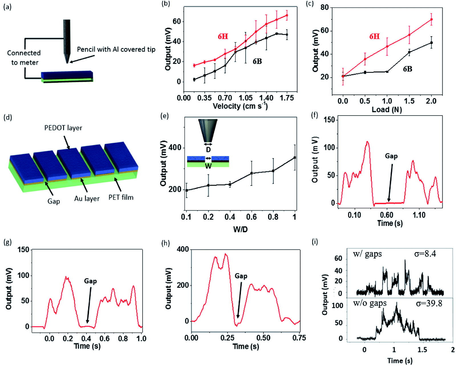 | ||
| Fig. 3 (a) Experimental setup using an Al covered pencil as a tip, (b) influence of the speed on the output signals generated by the 6B and 6H pencil devices, (c) influence of load on the potential output, (d) schematic of the testing device with gaps, (e) influence of the gap width on the output signals; (f)–(h) voltage profiles generated by the pencil at (f) 0.18 cm s−1 (g) 0.53 cm s−1 and (h) 1.4 cm s−1 speed at same location, (i) typical signal generated by scratching the devices with and without a gap. | ||
Speed and load weight sensing
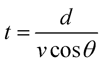
Apart from using a continuous PEDOT film, we used a patterned PEDOT film as an active layer. The patterned PEDOT film enabled the device to measure the sliding speed. Fig. 3(d) shows an example of the PEDOT film, which has periodically arranged gaps. When the Al tip moved to the edge of the PEDOT layer, the output value started reducing because of the decreased contact area. The output dropped to zero once the tip completely disconnected with PEDOT in the gap zone. Fig. 3(e) shows the influence of the gap width on the output signals. The ratio of the tip diameter (D) to the gap width (W) was calculated to indicate the contact area between the Al tip and PEDOT. Based on this feature, the speed of the underlying object can be estimated by measuring the time when the tip moved into and out of a gap. Herein, the time (t) required for the tip to travel through the gap can be described as follows:
 | (2) |
Fig. 3(i) provides a comparison of the outputs generated from a continuous PEDOT film and the film with five gaps (5 mm width). Herein, the standard error (σ) of each output was calculated. The σ of the output signals generated from the continuous PEDOT was 39.8 mV, whereas the σ of the output signals generated from the film with 5 gaps was 8.4 mV. The decrease in the volatility of the output suggests that more stable results are produced by the patterned PEDOT films.
Conclusions
We have shown that a Schottky contact consisting of a metal tip and a conducting polymer film can be used for sensing the touch and sliding movements. The output shows DC voltage features and is determined by the force applied to the conducting polymer layer, the travel speed of the metal tip and the profile of the conducting film. When a patterned conducting polymer film is employed, the movement speed of the metal tip can be estimated. The ability to detect the touch and sliding movements at different speeds and pressures together with the DC output makes the conducting polymer-metal Schottky contact very promising for the development of novel movement sensors.Conflicts of interest
There are no conflicts to declare.Acknowledgements
Funding support received from the Australian Research Council (ARC) through a Discovery Project (ARC DP140100079) is acknowledged.Notes and references
- H. M. Choset, Principles of robot motion: theory, algorithms, and implementation, MIT press, 2005 Search PubMed.
- S. Zolkiewski and D. Pioskowik, in New Perspectives in Information Systems and Technologies, Springer, 2014, vol. 1, pp. 593–604 Search PubMed.
- C. Wu, L. Peng, Z. Huang, M. Zhong and D. Chu, Transportation Research Part C: Emerging Technologies, 2014, 47, 179–191 CrossRef.
- A. Carullo and M. Parvis, IEEE Sens. J., 2001, 1, 143–147 Search PubMed.
- X. Mao, D. Inoue, S. Kato and M. Kagami, IEEE Transactions on Intelligent Transportation Systems, 2012, 13, 408–413 Search PubMed.
- R. Chambers, T. J. Gabbett, M. H. Cole and A. Beard, Sports Med., 2015, 45, 1065–1081 CrossRef PubMed.
- J. Lee, S. Kim, J. Lee, D. Yang, B. C. Park, S. Ryu and I. Park, Nanoscale, 2014, 6, 11932–11939 RSC.
- V. Lugade, E. Fortune, M. Morrow and K. Kaufman, J. Biomed. Eng., 2014, 36, 169–176 Search PubMed.
- Y. Yang, H. Zhang, J. Chen, Q. Jing, Y. S. Zhou, X. Wen and Z. L. Wang, ACS Nano, 2013, 7, 7342–7351 CrossRef CAS PubMed.
- T. Yamada, Y. Hayamizu, Y. Yamamoto, Y. Yomogida, A. Izadi-Najafabadi, D. N. Futaba and K. Hata, Nat. Nanotechnol., 2011, 6, 296–301 CrossRef CAS PubMed.
- B. Song, H. Choi and H. S. Lee, Surveillance tracking system using passive infrared motion sensors in wireless sensor network, in 2008 International Conference on Information Networking IEEE, 2008, pp. 1–5 Search PubMed.
- G. Gennarelli, G. Ludeno and F. Soldovieri, Remote Sens., 2016, 8, 621 CrossRef.
- D. S. Hecht, D. Thomas, L. Hu, C. Ladous, T. Lam, Y. Park, G. Irvin and P. Drzaic, J. Soc. Inf. Disp., 2009, 17, 941–946 CrossRef CAS.
- A. Holzinger, in Universal Access Theoretical Perspectives, Practice, and Experience: 7th ERCIM International Workshop on User Interfaces for All, Paris, France, October 24–25, 2002, Revised Papers, ed. N. Carbonell and C. Stephanidis, Springer Berlin Heidelberg, Berlin, Heidelberg, 2003, pp. 387–397, DOI:10.1007/3-540-36572-9_30.
- A. Al-Rahayfeh and M. Faezipour, IEEE Journal of Translational Engineering in Health and Medicine, 2013, 1, 2100212 Search PubMed.
- J. Yun and S.-S. Lee, Sensors, 2014, 14, 8057–8081 CrossRef PubMed.
- S. Ryu, P. Lee, J. B. Chou, R. Xu, R. Zhao, A. J. Hart and S.-G. Kim, ACS Nano, 2015, 9, 5929–5936 CrossRef CAS PubMed.
- P. Wolfendale, J. Phys. E: Sci. Instrum., 1968, 1, 817 CrossRef.
- P. B. Kosel, G. S. Munro and R. Vaughan, IEEE Trans. Instrum. Meas., 1981, IM-30, 114–123 Search PubMed.
- M. R. Bhalla and A. V. Bhalla, International Journal of Computer Applications, 2010, 6, 12–18 CrossRef.
- J. Chun, N.-R. Kang, J.-Y. Kim, M.-S. Noh, C.-Y. Kang, D. Choi, S.-W. Kim, Z. Lin Wang and J. Min Baik, Nano Energy, 2015, 11, 1–10 CrossRef CAS.
- T. Q. Trung and N.-E. Lee, Adv. Mater., 2016, 28, 4338–4372 CrossRef CAS PubMed.
- Z. L. Wang, Faraday Discuss., 2014, 176, 447–458 RSC.
- F.-R. Fan, L. Lin, G. Zhu, W. Wu, R. Zhang and Z. L. Wang, Nano Lett., 2012, 12, 3109–3114 CrossRef CAS PubMed.
- G. Zhu, W. Q. Yang, T. Zhang, Q. Jing, J. Chen, Y. S. Zhou, P. Bai and Z. L. Wang, Nano Lett., 2014, 14, 3208–3213 CrossRef CAS PubMed.
- Z. L. Wang and J. Song, Science, 2006, 312, 242–246 CrossRef CAS PubMed.
- A. Proto, M. Penhaker, D. Bibbo, D. Vala, S. Conforto and M. Schmid, Sensors, 2016, 16, 524 CrossRef PubMed.
- X. Wang, B. Yang, J. Liu and C. Yang, J. Mater. Chem. A, 2017, 5, 1176–1183 RSC.
- Y. S. Zhou, G. Zhu, S. Niu, Y. Liu, P. Bai, Q. Jing and Z. L. Wang, Adv. Mater., 2014, 26, 1719–1724 CrossRef CAS PubMed.
- H. Shao, J. Fang, H. X. Wang, L. M. Dai and T. Lin, Adv. Mater., 2016, 28, 1461–1466 CrossRef CAS PubMed.
- H. Shao, J. Fang, H. Wang, L. Dai and T. Lin, Adv. Mater., 2016, 28, 1461–1466 CrossRef CAS PubMed.
- W. Xu, C. Chang, Y. S. Hung, S. Kwan and P. C. W. Fung, IEEE Trans. Signal Process., 2007, 55, 5552–5563 Search PubMed.
Footnote |
| † Electronic supplementary information (ESI) available. See DOI: 10.1039/c9ra00120d |
| This journal is © The Royal Society of Chemistry 2019 |