
 Open Access Article
 This Open Access Article is licensed under a Creative Commons Attribution-Non Commercial 3.0 Unported Licence
AlN epitaxy on SiC by low-temperature atomic layer deposition via layer-by-layer, in situ atomic layer annealing
Wei-Chung Kao ,
Wei-Hao Lee,
Sheng-Han Yi,
Tsung-Han Shen,
Hsin-Chih Lin* and
Miin-Jang Chen*
,
Wei-Hao Lee,
Sheng-Han Yi,
Tsung-Han Shen,
Hsin-Chih Lin* and
Miin-Jang Chen*
Department of Materials Science and Engineering, National Taiwan University, 1, Roosevelt Rd, Sec. 4, Taipei 10617, Taiwan. E-mail: hclinntu@ntu.edu.tw; mjchen@ntu.edu.tw
First published on 17th April 2019
Abstract
AlN thin films were epitaxially grown on a 4H-SiC substrate via atomic layer deposition (ALD) along with atomic layer annealing (ALA). By applying the layer-by-layer, in situ ALA treatment using helium/argon plasma in each ALD cycle, the as-deposited film gets crystallization energy from the plasma, which results in significant enhancement of the crystal quality to achieve a highly crystalline AlN epitaxial layer at a deposition temperature as low as 300 °C. In a nanoscale AlN epitaxial layer with a thickness of ∼30 nm, X-ray diffraction reveals a low full-width-at-half-maximum of the AlN (0002) peak of only 176.4 arcsec. Atomic force microscopy, high-resolution transmission electron microscopy, and Fourier diffractograms indicate a smooth surface and high-quality hetero-epitaxial growth of a nanoscale AlN layer on 4H-SiC. This research demonstrates the impact of the ALA treatment on the evolution of ALD techniques from conventional thin film deposition to low-temperature atomic layer epitaxy.
Introduction
Aluminum nitride (AlN) has attracted great attention in academic and industrial fields as a result of its excellent properties including wide direct bandgap, high thermal conductivity, high piezoelectric response, good stability at high temperature, and chemical stability.1 Hence AlN has wide applications including in surface acoustic wave sensors (SAW),2 ultraviolet light-emitting diodes3 and dielectric layers.4 In addition, AlN thin films can be used as a buffer layer and the wetting agent for GaN epitaxial growth to reduce the mismatch of lattice constants and thermal expansion coefficients between GaN and the substrate.5–7AlN has been typically grown on Si, sapphire and silicon carbide (SiC) substrates, in which SiC has been regarded as the most favorable substrate due to its minimal lattice and thermal mismatch with AlN.8 Among the variety of SiC polytypes, the most common polymorphs developed for electronic applications are 4H-SiC and 6H-SiC. As compared with 6H-SiC, 4H-SiC has superior electron mobility, which is critical to high electron mobility transistors.9 Conventionally, AlN is grown by metal–organic chemical vapor deposition (MOCVD) and molecular beam epitaxy (MBE) at high temperatures over 900 °C to achieve highly crystalline epitaxial layers.10,11 However, these high-temperature growth techniques are challenged by the generation of misfit dislocations at AlN/SiC hetero-interface, which leads to high threading dislocation densities up to 108 cm2 for AlN grown on SiC.12
Atomic layer deposition (ALD) is an advanced technique for accurate preparation of high-quality nanoscale thin films. Based on self-limiting reactions and layer-by-layer growth mechanism, ALD is able to achieve atomically smooth surfaces, excellent conformity, low defect densities, and high uniformity over a large area.13,14 These benefits lead to a wide range of applications such as microelectronics,15,16 photovoltaics,17 energy storage18 and biomedical devices.19 For example, the high-k dielectrics prepared by ALD can improve the performance of 4H-SiC devices.20 However, ALD processes are typically conducted within a low temperature range referred as “ALD window” in order to avoid precursor decomposition or desorption, thereby achieving self-limiting deposition. As a result, thin films prepared by ALD are generally amorphous or poly-crystalline.14 However, it is well recognized that crystalline films have superior optical and electrical characteristics than amorphous films. For example, crystalline films have higher dielectric constant as compared with amorphous materials.21,22 Hence it is important and favorable to expand the ALD capacity to grow highly crystalline thin films. To enhance crystal quality, adequate energy is required for adatom migrations. Therefore, conventional material growth methods are often performed at high temperatures. Rather than high deposition temperatures, plasma treatment is an alternative way to deliver energy from incident ions to deposited film for adatom migration. As a matter of fact, dramatic improvement in crystal quality of thin films prepared by ALD has been demonstrated in our previous work by introducing the layer-by-layer, in situ Ar plasma treatment in each ALD cycle, which is technically termed as “atomic layer annealing (ALA)”.23 However, energetic Ar ion bombardment at high plasma power may induce damage to deposited films, giving rise to degradation of crystal quality.24
In this study, the ALA technique is modified by helium/argon (He/Ar) mixture plasma to achieve hetero-epitaxial growth of a nanoscale AlN layer on SiC at a deposition temperature as low as 300 °C. He plasma not only deals less damage compared to Ar plasma because of the smaller mass and momentum of He ions,25 but also facilitates Ar ionization as a result of the Penning effect.26 A high-quality AlN epilayer of only ∼30 nm in thickness is evidenced by a low full width at half-maximum (FWHM) of only 176.4 arcsec in the X-ray ω-scan rocking curve and a clear diffractogram in the high-resolution transmission electron microscopy (HRTEM) image. The satellite peaks in the θ–2θ X-ray diffraction (XRD) pattern indicates a smooth surface, which is confirmed by atomic force microscopy (AFM). These results demonstrate that the ALA process with He/Ar plasma treatment in each ALD cycle is a highly effective technique for realizing high-quality hetero-epitaxy at low growth temperatures.
Experiments
The AlN layers were deposited on 4H-SiC wafer (commercial semi-insulating (0001) 4H-SiC wafers with 4° off-axis) at a low temperature of 300 °C by ALD (Cambridge Nanotech Fiji G2). Trimethylaluminum (TMA) was used as the metal–organic precursor and nitrogen (N2)/hydrogen (H2) plasma were used as the reactant. As schematically illustrated in Fig. 1, the conventional ALD cycle consists of the following 4 steps: (1) TMA pulse, (2) Ar purge, (3) N2/H2 plasma, and (4) Ar purge. The ALA process with an additional step (5) He/Ar or Ar plasma treatment (20 s) was introduced after the step (4) to provide energy for adatom migration. Therefore, each as-deposited monolayer prepared by the conventional ALD cycle is modified by the He/Ar or Ar ion bombardment during the step (5). In this study, the ratio (50%) of the partial pressure of He to the total pressure of He and Ar was used in the He/Ar plasma. A reference AlN sample was prepared without the ALA treatment for comparison. In order to investigate the electrical properties of the AlN layers, the metal–insulator–semiconductor (MIS) structures were fabricated on the commercial N-type (0001) 4H-SiC wafers (4° off-axis) with a high doping concentration of ∼1 × 1018 cm−3. The thicknesses of all the AlN layers (the reference AlN and the AlN layers treated with the Ar plasma and the He/Ar plasma, respectively) are ∼29.9 nm, which were confirmed by the spectroscopic ellipsometry. Platinum was then deposited on the AlN layers by sputtering as the top electrodes with a diameter of 300 μm. The backside ohmic contact was coated with 100 nm aluminum via thermal evaporation.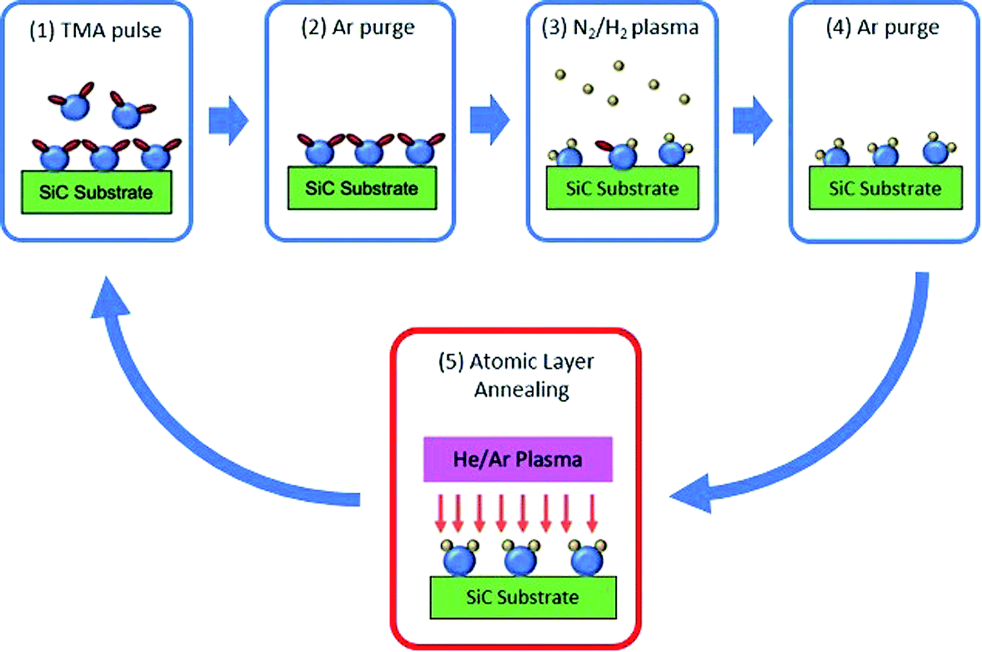 | ||
| Fig. 1 The schematic diagram of the processing cycle including the atomic layer annealing (ALA) to achieve low-temperature epitaxial growth of AlN on SiC. The conventional ALD cycle contains steps (1)–(4). The ALA treatment is introduced in step (5) with the in situ He/Ar or Ar plasma treatment to facilitate adatom migration for improving the crystalline quality of the AlN layer. The reference AlN sample was deposited without the step (5). | ||
To examine the crystallinity of AlN layers, XRD was performed by PANalytical X'Pert Pro MRD X-ray diffractometer in θ–2θ and ω-scan (rocking curve) modes. AFM was carried out using a Veeco D5000 scanning probe microscope to probe the surface morphology and the roughness of AlN layers. The microstructure of AlN layers and the interface between AlN and SiC were analyzed by HRTEM using JEOL JEM-2100F TEM with an acceleration voltage of 200 kV and Philips Tecnai F30 FEG-TEM with an acceleration voltage of 300 kV. The spectroscopic ellipsometer (SE, Elli-SE, Ellipso Technology) was used to measure the AlN thickness on the SiC substrate. The capacitance–voltage (C–V) and current–voltage (I–V) measurements were performed using the Keysight B1500A semiconductor device parameter analyzer to investigate the electrical characteristics of the MIS capacitors.
Results and discussion
Fig. 2 shows the θ–2θ XRD patterns of the reference AlN sample and the AlN layers prepared with the ALA treatments using layer-by-layer, in situ Ar and He/Ar plasma, respectively, at a radio-frequency (RF) power of 300 W. The significant peak at 2θ ∼ 35.5° corresponds to SiC(0004) and the peak at 2θ ∼ 36° indicates AlN(0002) of wurtzite structure. Compared with the reference AlN sample, the AlN(0002) peak intensity of the ALA-treated AlN layers is significantly enhanced, which indicates the considerable improvement of crystallinity by the ALA treatments using Ar and He/Ar plasma. The enhancement of crystal quality is attributed to surface crystallization and surface heating as a result of energy transfer from the plasma to each as-deposited monolayer.23 The AlN(0002) peak of the AlN layer prepared with the He/Ar plasma treatment is more significant than that prepared with the Ar plasma treatment, revealing the He/Ar plasma is more beneficial to the AlN crystal quality. The outcome might result from less plasma damage caused by helium due to its smaller atomic mass. In addition, because of the higher metastable state of He than that of Ar, the energy transfer via collisions of He* with Ar gives rise to an increases of the Ar ionization rate (the so-called Penning effect), which is described as follows:26| He* + Ar → He + Ar+ + e− |
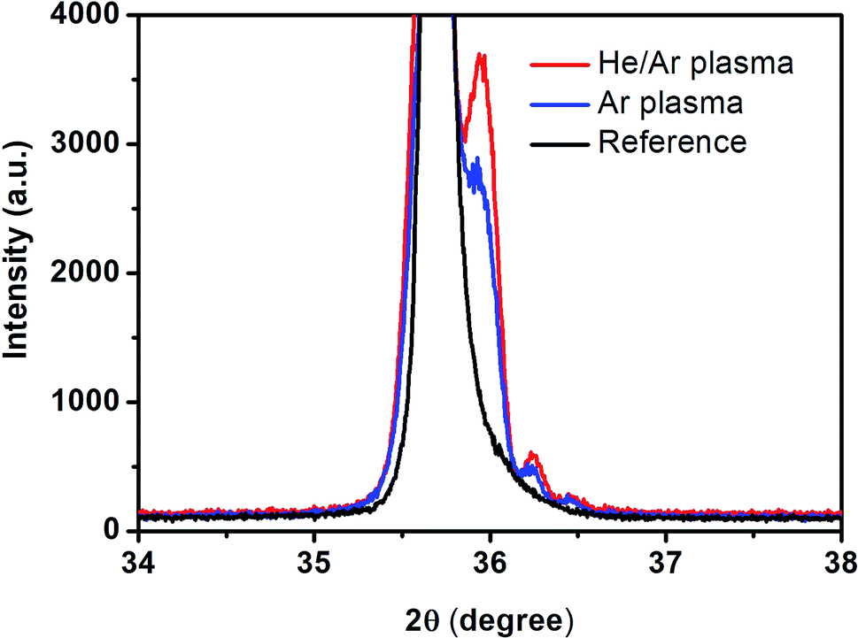 | ||
| Fig. 2 The θ–2θ XRD patterns of the reference AlN sample and the AlN layers treated in situ by ALA with the Ar and He/Ar plasma in each ALD cycle. The significant AlN(0002) peak at 2θ ∼ 36° of the AlN layer prepared with the He/Ar plasma treatment indicates the ALA treatment is effective for the improvement of the AlN crystal quality. | ||
Notice that multiple satellite peaks are observed in Fig. 2 near the AlN(0002) peak of the AlN layers treated with the Ar and He/Ar plasma. These satellite peaks might be ascribed to the interference from the surface and the interface between the substrate and the ultra-thin hetero-epitaxial layer,27 indicating that the AlN layer treated with the ALA process has high crystallinity and smooth surface.
Fig. 3 reveals the XRD ω-scan rocking curves of the reference AlN sample and the AlN layers prepared with the ALA treatments using layer-by-layer, in situ He/Ar plasma at RF powers of 50 and 300 W, respectively. The peak at ω ∼ 18.01° originates from AlN(0002) and the peak around ω ∼ 17.84° can be attributed to the diffraction from SiC(0004) since the XRD peak of SiC(0004) (2θ ∼ 35.5°) is close to the AlN(0002) peak (2θ ∼ 36°). The FWHMs of AlN(0002) rocking curves are 258.6, 235.1, and 176.4 arcsec, respectively, for the reference AlN sample and the AlN layers prepared at RF plasma powers of 50 and 300 W. With the RF plasma power at 50 W, the ALA treatment shows minimal improvement in epitaxial quality of the AlN layer. An increase of the RF plasma power from 50 W to 300 W results in a notable decrease of the FWHM of only 176.4 arcsec, indicating significant enhancement of crystallinity of the AlN layer by the ALA treatment. Fig. 2 and 3 clearly demonstrate that the ALA treatment with the He/Ar mixture plasma is capable of significantly improving the epitaxial quality of AlN layers, achieving a high-quality ultrathin (∼30 nm) AlN epilayer at a growth temperature as low as 300 °C.
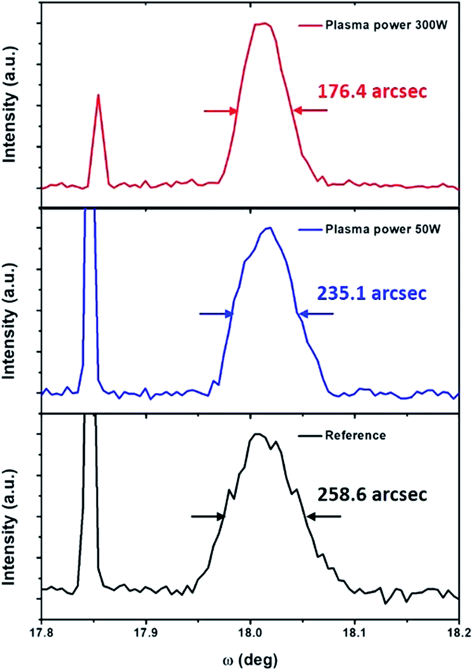 | ||
| Fig. 3 The XRD ω-scan rocking curves of the (0002) peak of the reference AlN sample and the AlN layers treated with the in situ He/Ar plasma at plasma powers of 50 and 300 W, respectively. A low FWHM (176.4 arcsec) of the AlN(0002) rocking curves indicates high crystal quality of the nanoscale AlN epilayer prepared with the ALA treatment. | ||
Fig. 4 displays the AFM images of the 4H-SiC wafer, the reference AlN sample and the AlN layers prepared with the ALA treatments using the layer-by-layer, in situ Ar and He/Ar plasma, respectively, at a RF power of 300 W. The root-mean-square (RMS) surface roughness of the SiC wafer is 0.15 nm (Fig. 4(a)). For the reference AlN sample and the AlN layer treated with the Ar plasma, the RMS surface roughness is increased respectively to 0.41 and 0.74 nm, as shown in Fig. 4(b) and (c). The increase of surface roughness is attributed to the grain growth of AlN. Fig. 4(d) shows that the He/Ar plasma ALA treatment on the AlN layer leads to a decrease of the RMS surface roughness to 0.31 nm. The He/Ar plasma ALA treatment promotes adatom diffusion and rearrangement, thereby leading to the smooth and uniform surfaces of the AlN layer.
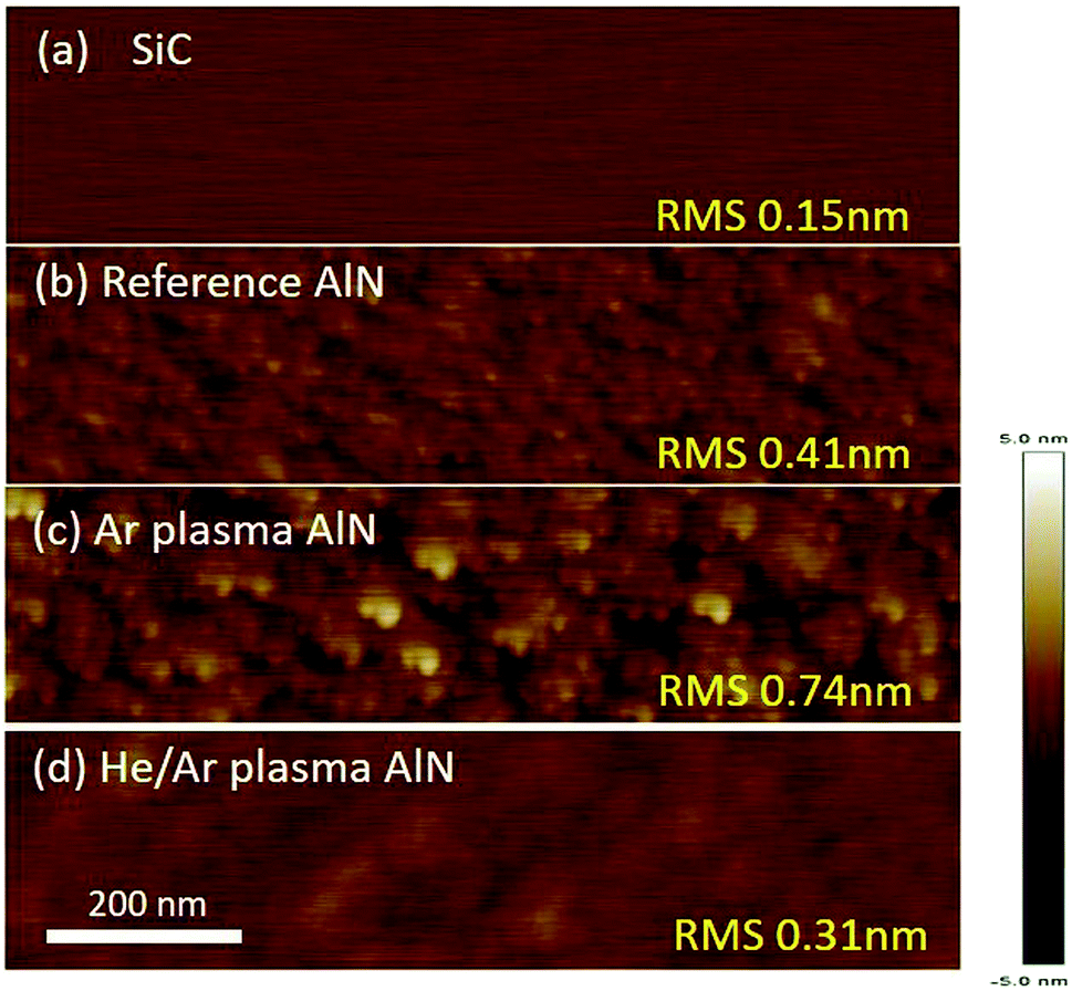 | ||
| Fig. 4 AFM images of (a) the SiC wafer, (b) the reference AlN sample, (c) the AlN layer treated with the Ar plasma, and (d) the AlN layer treated with the He/Ar plasma. The in situ He/Ar plasma treatment leads to a decrease of the RMS surface roughness of the AlN layer. | ||
HRTEM observation was carried out to investigate the microstructure and interface of AlN layers on 4H-SiC substrate. Fig. 5(a) and (d) display the cross-sectional HRTEM images of the AlN/SiC hetero-interface, in which the AlN layers are the reference AlN (Fig. 5(a)) and that prepared with the ALA treatment using layer-by-layer, in situ He/Ar plasma, respectively. The fast Fourier transform (FFT) diffractograms of the enclosed regions in AlN and SiC are shown respectively in Fig. 5(b, c) and (e, f). The HRTEM image of the ALA-treated AlN layer (Fig. 5(d)) reveals significantly improved crystal quality without misorientation compared to the HRTEM image of the reference AlN sample (Fig. 5(a)). This is supported by the clear FFT diffractograms of AlN in Fig. 5(e) in contrast to Fig. 5(b). A comparison of FFT diffractograms of the ALA-treated AlN layer and SiC in Fig. 5(e) and (f) reveals the epitaxial orientation between AlN and the substrate: [0001]AlN//[0001]SiC and [11![[2 with combining macron]](https://www.rsc.org/images/entities/char_0032_0304.gif) 0]AlN//[110]SiC. The result demonstrates that the ALA-treated AlN epilayer exhibits a highly crystalline hexagonal structure with [0001] preferred orientation perpendicular to the SiC surface.
0]AlN//[110]SiC. The result demonstrates that the ALA-treated AlN epilayer exhibits a highly crystalline hexagonal structure with [0001] preferred orientation perpendicular to the SiC surface.
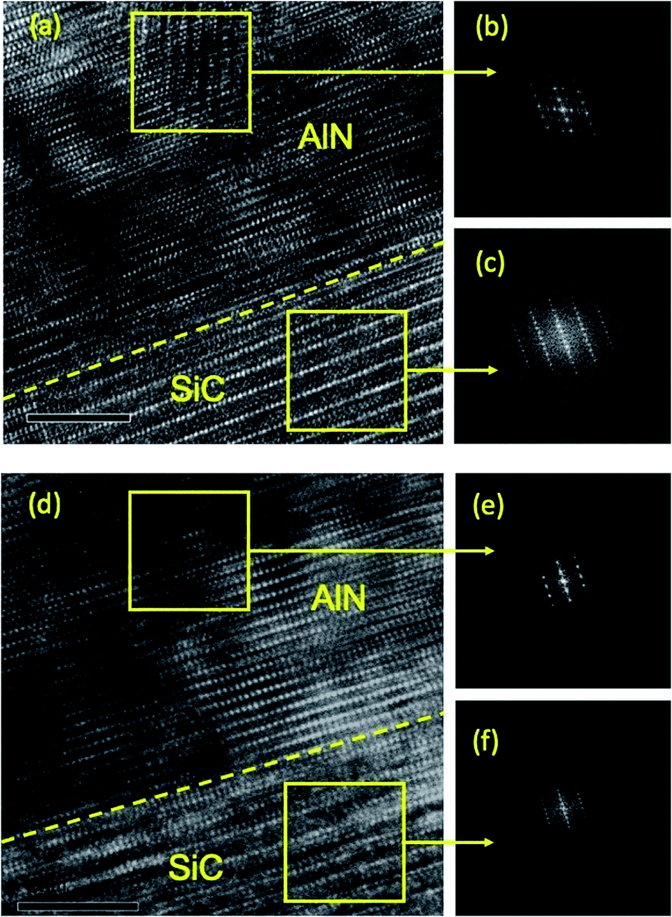 | ||
| Fig. 5 (a) Cross-sectional HRTEM image of the reference AlN layer deposited on SiC substrate. (b and c) The FFT diffractograms of the regions enclosed in the AlN layer and SiC, respectively. (d) Cross-sectional HRTEM image of the AlN/SiC hetero-interface, where the AlN layer was prepared with the ALA treatment using layer-by-layer, in situ He/Ar plasma at a plasma power of 300 W. (e and f) The FFT diffractograms of the regions enclosed in the AlN layer and SiC, respectively. The result indicates that the ALA process leads to high-quality epitaxial growth of AlN on SiC at a low temperature of 300 °C. | ||
Fig. 6(a) shows the C–V characteristics (100 kHz) of the MIS capacitors with forward and backward voltage sweeping from −10 V to +10 V. Since the SiC wafer is heavily doped, it is difficult to induce a wide depletion layer in SiC. Thus the capacitance is not depleted to a small value as a negative voltage is applied to the top electrode. The stretch-out/distortion of the C–V curve of the reference AlN sample might be caused by the interfacial states at the AlN/SiC interface.28,29 Hence the improved C–V characteristics suggest a decrease in the interfacial state density by the Ar and He/Ar plasma ALA treatment. The maximum capacitance in the C–V curves can give an estimation of the AlN dielectric constants, which are ∼7.9, 8.6, and 9.1 for the reference AlN and the AlN layers treated with the Ar and He/Ar plasma, respectively. The increase of dielectric constant is associated with the enhancement of crystallinity of the AlN layers due to the ALA treatment.21 The hysteresis of the C–V curves reveals the presence of slow interfacial traps or defects which can not follow the change in the applied voltage.30 The leakage current density as a function of applied voltage is shown in Fig. 6(b). The AlN layers prepared with the Ar and He/Ar plasma ALA treatments exhibit higher leakage current densities than the reference AlN sample, which could be ascribed to the presence of leakage current paths through grain boundaries as a result of the enhanced crystallinity.31–33
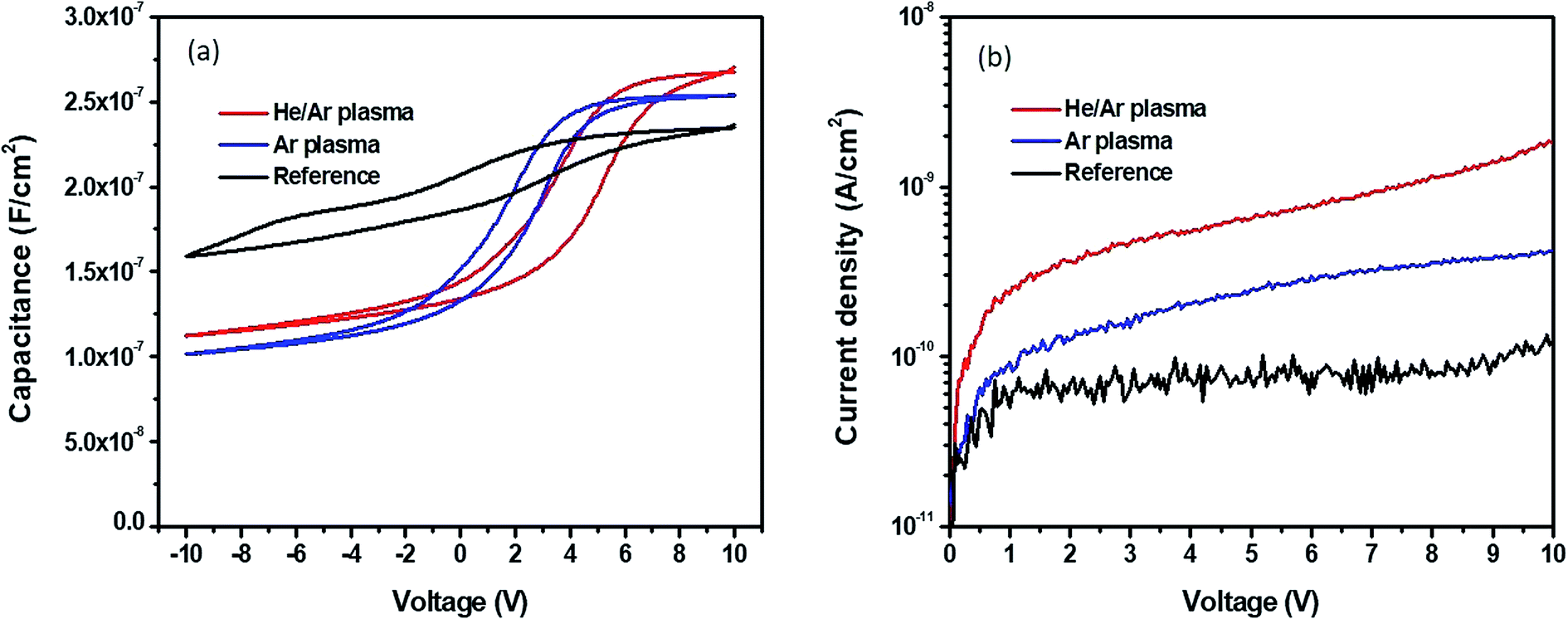 | ||
| Fig. 6 (a) C–V and (b) I–V characteristics of the MIS capacitors with the reference AlN and the AlN layers treated with the Ar and He/Ar plasma. The voltage is applied to the top electrode. The Ar and He/Ar plasma ALA treatments give rise to an enhancement of the capacitance and an increase of leakage current density of the AlN layers. | ||
Conclusions
In summary, by applying the ALA technique based on the layer-by-layer, in situ He/Ar plasma treatment in each ALD cycle, the epitaxial growth of a high-quality nanoscale AlN layer on 4H-SiC substrate is achieved at a low deposition temperature of only 300 °C. The XRD, AFM, and HRTEM characterizations reveal a high-quality hexagonal AlN epilayer (of only ∼30 nm in thickness) with a smooth surface and a low FWHM of only 176.4 arcsec in the X-ray rocking curve. The ALA technique pushes the boundary of ALD techniques from deposition of amorphous/poly-crystalline thin films to epitaxial growth of highly crystalline layers at a low temperature, which opens a variety of practical applications and research fields in the near future.Conflicts of interest
There are no conflicts to declare.Acknowledgements
The authors acknowledge the partially financial support in part by the Ministry of Science and Technology, Taiwan (107-2218-E-002-045 and 106-2622-E-002-006-CC2).Notes and references
- S. Strite and H. Morkoç, J. Vac. Sci. Technol., B: Microelectron. Nanometer Struct.–Process., Meas., Phenom., 1992, 10, 1237–1266 CrossRef CAS.
- H. Okano, N. Tanaka, Y. Takahashi, T. Tanaka, K. Shibata and S. Nakano, Appl. Phys. Lett., 1994, 64, 166–168 CrossRef CAS.
- Y. Taniyasu, M. Kasu and T. Makimoto, Nature, 2006, 441, 325 CrossRef CAS PubMed.
- A. Chin, C. Lai, B. Hung, C. Cheng, S. P. McAlister, C. Zhu, M.-F. Li and D.-L. Kwong, A novel program-erasable high-k AlN capacitor with memory function, Non-Volatile Memory Technology Symposium, IEEE, 2004, pp. 18–23 Search PubMed.
- G. W. Auner, F. Jin, V. M. Naik and R. Naik, J. Appl. Phys., 1999, 85, 7879–7883 CrossRef CAS.
- Y.-Y. Wong, Y.-S. Chiu, T.-T. Luong, T.-M. Lin, Y.-T. Ho, Y.-C. Lin and E. Y. Chang, Growth and fabrication of AlGaN/GaN HEMT on SiC substrate, 2012 10th IEEE International Conference on Semiconductor Electronics (ICSE), IEEE, 2012, pp. 729–732 Search PubMed.
- B. Zhang, M. Wu, X. Shen, J. Chen, J. Zhu, J. Liu, G. Feng, D. Zhao, Y. Wang and H. Yang, J. Cryst. Growth, 2003, 258, 34–40 CrossRef CAS.
- F. Ponce, B. Krusor, J. Major Jr, W. Plano and D. Welch, Appl. Phys. Lett., 1995, 67, 410–412 CrossRef CAS.
- C. Codreanu, M. Avram, E. Carbunescu and E. Iliescu, Mater. Sci. Semicond. Process., 2000, 3, 137–142 CrossRef CAS.
- K. Uehara, C.-M. Yang, T. Furusho, S.-K. Kim, S. Kameda, H. Nakase, S. Nishino and K. Tsubouchi, AlN epitaxial film on 6H-SiC (0001) using MOCVD for GHz-band saw devices, 2003 IEEE Ultrasonics Symposium, IEEE, 2003, pp. 905–908 Search PubMed.
- S. Tanaka, R. S. Kern and R. F. Davis, Appl. Phys. Lett., 1995, 66, 37–39 CrossRef CAS.
- Y. Taniyasu, M. Kasu and T. Makimoto, J. Cryst. Growth, 2007, 298, 310–315 CrossRef CAS.
- S. M. George, Chem. Rev., 2009, 110, 111–131 CrossRef PubMed.
- M. Leskelä and M. Ritala, Thin Solid Films, 2002, 409, 138–146 CrossRef.
- E. Gusev, C. Cabral Jr, M. Copel, C. D'emic and M. Gribelyuk, Microelectron. Eng., 2003, 69, 145–151 CrossRef CAS.
- B. Choi, D. Jeong, S. Kim, C. Rohde, S. Choi, J. Oh, H. Kim, C. Hwang, K. Szot and R. Waser, J. Appl. Phys., 2005, 98, 033715 CrossRef.
- B. Hoex, S. Heil, E. Langereis, M. Van de Sanden and W. Kessels, Appl. Phys. Lett., 2006, 89, 042112 CrossRef.
- S. Boukhalfa, K. Evanoff and G. Yushin, Energy Environ. Sci., 2012, 5, 6872–6879 RSC.
- P. Chen, T. Mitsui, D. B. Farmer, J. Golovchenko, R. G. Gordon and D. Branton, Nano Lett., 2004, 4, 1333–1337 CrossRef CAS PubMed.
- E. Schilirò, R. Lo Nigro, P. Fiorenza and F. Roccaforte, AIP Adv., 2016, 6, 075021 CrossRef.
- G. Lupina, G. Kozlowski, P. Dudek, J. Dabrowski, C. Wenger, G. Lippert and H.-J. Mussig, Dielectric characteristics of amorphous and crystalline BaHfO3 high-k layers on TiN for memory capacitor applications, 2008 9th International Conference on Ultimate Integration of Silicon, IEEE, 2008, pp. 159–162 Search PubMed.
- J.-J. Huang, L.-T. Huang, M.-C. Tsai, M.-H. Lee and M.-J. Chen, ECS J. Solid State Sci. Technol., 2013, 2, P524–P528 CrossRef CAS.
- H.-Y. Shih, W.-H. Lee, W.-C. Kao, Y.-C. Chuang, R.-M. Lin, H.-C. Lin, M. Shiojiri and M.-J. Chen, Sci. Rep., 2017, 7, 39717 CrossRef CAS PubMed.
- X. Cao, S. Pearton, A. Zhang, G. Dang, F. Ren, R. Shul, L. Zhang, R. Hickman and J. Van Hove, Appl. Phys. Lett., 1999, 75, 2569–2571 CrossRef CAS.
- J. Holgado, A. Barranco, F. Yubero, J. Espinos and A. González-Elipe, Nucl. Instrum. Methods Phys. Res., Sect. B, 2002, 187, 465–474 CrossRef CAS.
- E. E. Ferguson, Phys. Rev., 1962, 128, 210 CrossRef CAS.
- M. Liu and H. K. Kim, Appl. Phys. Lett., 2004, 84, 173–175 CrossRef CAS.
- K. Druijf, J. De Nijs, E. Drift, E. Granneman and P. Balk, Appl. Phys. Lett., 1994, 65, 347–349 CrossRef CAS.
- T. J. Mego, Rev. Sci. Instrum., 1986, 57, 2798–2805 CrossRef CAS.
- M. Aboelfotoh, R. Kern, S. Tanaka, R. Davis and C. Harris, Appl. Phys. Lett., 1996, 69, 2873–2875 CrossRef CAS.
- H.-W. Zan, K.-H. Yen, P.-K. Liu, K.-H. Ku, C.-H. Chen and J. Hwang, Org. Electron., 2007, 8, 450–454 CrossRef CAS.
- C.-M. Zetterling, M. Östling, K. Wongchotigul, M. Spencer, X. Tang, C. Harris, N. Nordell and S. Wong, J. Appl. Phys., 1997, 82, 2990–2995 CrossRef CAS.
- A. Noreika, M. Francombe and S. Zeitman, J. Vac. Sci. Technol., 1969, 6, 194–197 CrossRef CAS.
| This journal is © The Royal Society of Chemistry 2019 |