
 Open Access Article
 This Open Access Article is licensed under a Creative Commons Attribution-Non Commercial 3.0 Unported Licence
Reduced graphene oxide decorated with octahedral NiS2/NiS nanocrystals: facile synthesis and tunable high frequency attenuation†
Min Lu‡
a,
Na Gao‡bc,
Xiao-Juan Zhang*c and
Guang-Sheng Wang *bc
*bc
aSchool of Chemical Engineering, Northeast Electric Power University, Jilin 132000, P. R. China
bSchool of Chemistry, Beihang University, Beijing 100191, P. R. China. E-mail: wanggsh@buaa.edu.cn
cSchool of Physics and Nuclear Energy Engineering, Beihang University, Beijing 100191, P. R. China. E-mail: zhxiaojuan@buaa.edu.cn
First published on 13th February 2019
Abstract
Reduced graphene oxide (RGO) decorated with octahedral NiS2/NiS nanocrystals were fabricated via a facile synthetic strategy. By appropriate adjustment of the weight ratio of GO and NiS2/NiS nanocrystals, RGO–NiS2/NiS nanocomposites with an excellent microwave absorption performance were achieved. As expected, RGO–NiS2/NiS nanocomposites in a polyvinylidene fluoride (PVDF) matrix with different mass fractions (5, 10, 15, 20 wt%) possess effective absorption in the high frequency range with a thin thickness (1.5 mm) compared with those of octahedral NiS2/NiS nanocrystals. It was revealed that RGO–NiS2/NiS nanocomposites with a GO![[thin space (1/6-em)]](https://www.rsc.org/images/entities/char_2009.gif) :NiS2/NiS weight ratio of 1:4 exhibited the most prominent microwave absorption property. The optimal effective frequency bandwidth of this sample covers 4.32 GHz at a thin coating layer of 1.5 mm (15 wt%). The corresponding reflection loss value can reach −32.2 dB at 14.32 GHz. Moreover, the fundamental attenuation mechanisms are also discussed in detail.
:NiS2/NiS weight ratio of 1:4 exhibited the most prominent microwave absorption property. The optimal effective frequency bandwidth of this sample covers 4.32 GHz at a thin coating layer of 1.5 mm (15 wt%). The corresponding reflection loss value can reach −32.2 dB at 14.32 GHz. Moreover, the fundamental attenuation mechanisms are also discussed in detail.
Introduction
Currently, with the rapid rise of information technology and extensive use of electronic devices, serious electromagnetic interference (EMI) and EM pollution derived from these devices have gained increased attention. In order to solve such problems, tremendous effort has been devoted to fabrication of high-performance microwave absorbers used in the fields of electronic reliability, healthcare and national defence security.1–3 Generally speaking, the ideal EM wave absorption materials are primarily concerned with satisfying the requirements of intense absorption ability and broad absorption bandwidth. Additionally, for practical applications, suitable microwave absorbers should possess some other important features including lightweight and thin thickness.4,5 It is well known that microwave absorption properties are related to complex permittivity and permeability
  , as well as their impedance matching. These electromagnetic parameters can be effectively tuned by modifying the chemical composition or filler loading content.6,7
To date, transition metal sulfides (TMSs) and their composites have been studied extensively for their application as catalysts,8–10 batteries,11–13 energy conversion14 and supercapacitors.15,16 In addition, many researchers have explored their application in the microwave-absorbing field because of their remarkable microwave absorption performance. Compared with transition metal oxides (TMOs), TMSs as an important class of inorganics, usually exhibit higher conductivity and better dielectric loss which are beneficial to obtaining high-performance absorbing materials.13,17 For instance, Ning et al.18 have prepared few-layered MoS2 nanosheets (MoS2-NS) and investigated their microwave absorption properties. The results indicate that the minimum reflection loss (RL) value of MoS2-NS/wax with 60 wt% loading is −38.42 dB at a thickness of 2.4 mm, which is almost 4 times higher than that of MoS2-bulk/wax. Zhao and co-workers2 have constructed hierarchical hollow CuS microspheres and found that the minimum reflection loss of paraffin-based composites (50 wt%) is −17.5 dB and the effective bandwidth is 3.0 GHz with thin absorber thickness of 1.1 mm. Other metal sulfides such as CdS,19 Bi2S3,20 CoS,21 PbS,22 NiS2@MoS2,23 etc. have been demonstrated as novel microwave absorbers with a remarkable reflection loss. Among these metal sulfides, investigations of the microwave absorption properties of nickel sulfides are scarce.
Although TMSs possess a relatively better conductive ability than its oxide counterpart, it is difficult to achieve excellent microwave absorbers from a single material. Therefore, the hybridization of different materials with various properties is being deeply considered. Recently, graphene or graphene derivatives have attracted considerable attention for electromagnetic wave suppression due to their unique physical, chemical, and mechanical properties including low density, high specific surface area, excellent electronic conductivity and versatile processing.24,25 Wen et al.26 have contrastively studied the absorbing properties of reduced graphene oxide (r-GO) and graphite nanosheets (GN) and the results suggest that r-GOs are the thinnest and most lightweight materials with highly efficient microwave attenuation performances of the carbon world. In addition, plenty of graphene-based composites such as graphene/SiC nanowire foam composites,27 air@rGO@Fe3O4 microspheres,28 CoS2/rGO nanohybrids,29 RGO/CuS or RGO/MoS2 nanocomposites30,31 etc. have also been investigated as effective microwave absorbers. In addition, Ji and his group32 have reviewed the evolution of graphene-based electromagnetic absorption materials and discussed the related electromagnetic attenuation theory in detail. Thus, it is well known that the combination of TMSs and graphene is an effective method for preparing high-performance EM wave absorbing materials.
In this article, the octahedral NiS2/NiS nanocrystals were fabricated via a facile solvothermal route and then combined with reduced graphene oxide (RGO) to form RGO–NiS2/NiS nanocomposites. On the one hand, the addition of NiS2/NiS nanocrystals may avoid the agglomeration of RGO. On the other hand, the introduction of RGO would ensure the composites possess remarkable absorbing properties at low filler content and thin thickness. The experimental results showed that the RGO–NiS2/NiS nanocomposites with a GO:NiS2/NiS weight ratio of 1:4 achieved the strongest EM wave absorption. The minimum RL value decreased rapidly to −32.2 dB at 14.32 GHz with a thin layer thickness of 1.5 mm when the filler loading was 15 wt%, and the effective frequency bandwidth covered 4.32 GHz. Meanwhile, when the weight ratio changed to 1:1, the minimum RL value reached −24.3 dB (13.44 GHz) with a thickness of 2.0 mm when the filler content was only 5 wt% and the effective frequency bandwidth was up to 4.72 GHz.
Results and discussion
To study the crystal structures of all samples, the XRD patterns have been provided in Fig. 1. On the XRD pattern of the octahedral NiS2/NiS nanocrystals shown in Fig. 1a, it can be seen that the dominant phase is vaesite NiS2 (cubic structure, JCPDS no. 11-0099) together with a small amount of NiS (hexagonal structure, JCPDS no. 02-1280). The narrow sharp peaks confirm that the nanocrystals are composed of highly crystallized NiS2 and NiS without any other impurities. As shown in Fig. 1b, the diffraction peak appears at 2θ = 10.6° corresponding to the (001) plane of GO. Moreover, the XRD patterns of RGO–NiS2/NiS nanocomposites (S2–S5) are almost the same as that of NiS2/NiS nanocrystals. The absence of the X-ray diffraction peak for GO around 10.6° in these samples and the broad peak at 2θ = 24.3° for S2 indicate that GO can be reduced to RGO effectively. | ||
| Fig. 1 XRD pattern of (a) NiS2/NiS nanocrystals (S1); (b) GO and RGO–NiS2/NiS nanocomposites (S2–S5). | ||
The morphology of the as-synthesized NiS2/NiS nanocrystals and RGO–NiS2/NiS nanocomposites were characterized by SEM observation. Fig. 2a–e shows the corresponding SEM images of S1–S5 which exhibit a typical octahedral architecture. After introducing RGO, from the overview images, it was found that the NiS2/NiS nanocrystals can be coated by RGO uniformly. Meanwhile, the NiS2/NiS nanocrystals could effectively avoid agglomeration of RGO nanosheets. The crinkled and flexible RGO surface is beneficial to increasing interface areas between RGO sheets and NiS2/NiS nanocrystals. Moreover, the FESEM characterization and the corresponding elemental maps of S2 have been displayed in Fig. 2f. In the rectangular region, the elemental maps of Ni, S and C demonstrate a good dispersion of NiS2/NiS nanocrystals in RGO sheets.
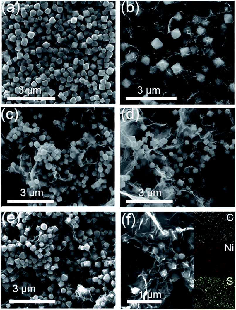 | ||
| Fig. 2 SEM images of (a) S1, (b) S2, (c) S3, (d) S4, (e) S5; (f) FESEM image of S2 and corresponding elemental mapping images of Ni and S. | ||
X-ray photoelectron spectroscopy (XPS) measurements were performed to further certify the existence of NiS2 and NiS. The Ni 2p spectrum can be divided into two spin–orbit doublets and two shake-up satellites (Fig. 3a). The peaks at 855.8 and 874.9 eV were attributed to 2p3/2 and 2p1/2 of Ni2+, and the peaks at 853.1 and 873.1 eV were assigned to 2p3/2 and 2p1/2 of Ni3+. The existence of Ni3+ was attributed to the slight oxidation of NiS2/NiS nanocrystals on the surface. For the S 2p spectrum (as shown in Fig. 3b), the peaks at 161.2 and 162.3 eV were assigned to S 2p3/2 and S 2p1/2 of Ni–S bonding, while the peaks at 163.5 and 168.0 eV correspond to the divalent sulfide ions (S22−) and sulfates with high oxidation state, respectively.33,34 The atomic percentages of Ni and S are shown in Table S1.† Additionally, Raman spectroscopy was used to analyze the graphitization degree of GO/RGO and the interaction between RGO and the nickel sulfides. Fig. S1a† shows the Raman spectra of GO and RGO–NiS2/NiS nanocomposites. It is clear that these Raman spectra exhibit two regular peaks, corresponding to the G band (∼1573 cm−1) and D band (∼1347 cm−1), respectively. The G-band represents the stretching vibration mode in the sp2-hybridized C–C bonds, while the D band corresponds to the first-order zone boundary phonon mode associated with defects or lattice distortion.35 Commonly, the ratios of intensity between the D and G bands (ID/IG) demonstrates the disorder degree of the graphitic layers. Here, the ID/IG ratios for S2–S5 are higher than that of GO (1.04), suggesting a higher degree of defects in RGO–NiS2/NiS nanocomposites or the edges due to the reduction process and introduction of the NiS2/NiS nanocrystals. To further determine the composition, Fig. S1b† shows EDS results of NiS2/NiS nanocrystals, which verifies the presence of elemental Ni and S in the sample.
 | ||
| Fig. 3 XPS spectra of (a) Ni 2p and (b) S 2p in NiS2/NiS nanocrystals. | ||
As is well known, microwave absorption properties of an absorber are highly associated with its complex permittivity and complex permeability, where the real parts of complex permittivity (ε′) and complex permeability (μ′) symbolize the storage capability of electric and magnetic energy, and imaginary parts (ε′′ and μ′′) are related to the dissipation of energy and magnetic loss, respectively.36 By mixing various samples (S1–S5) with PVDF, the EM wave absorption performance of these composites were investigated in terms of reflection loss (RL). On the basis of the measured data of the complex permittivity and complex permeability, the RL values can be calculated according to the transmission line theory, which is summarized by the following equations:37
 | (1) |
 | (2) |
:NiS2/NiS weight ratio of 1:4 achieve stronger EM wave absorption. The minimum RL value decreases rapidly to −32.2 dB at 14.32 GHz with a thin layer thickness of 1.5 mm when the filler loading is 15 wt%, and the effective frequency bandwidth is from 12.56 to 16.88 GHz (4.32 GHz). In addition, the layer thickness d also plays an important role in tuning the EM wave response characteristic. Comparing Fig. 4c and 5c, it is clear that the thickness can greatly influence the RL value and effective frequency bandwidth. It is seen that the S5 displays an optimum RL value of −28.7 dB at 10.48 GHz with a thin layer thickness of 2.0 mm, and the effective absorption bandwidth covers 2.8 GHz. In practical applications, in order to obtain lightweight materials, it is desirable that the filling amount is as low as possible. As shown in Fig. 5a, the minimum RL value appears at 13.44 GHz (−24.3 dB) with a thickness of 2.0 mm when the filler content is only 5 wt% for S3 and the effective frequency bandwidth is up to 4.72 GHz (11.52–16.24 GHz).
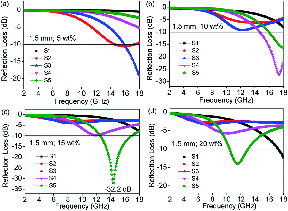 | ||
| Fig. 4 Microwave RL curves of the S1–S5 with loading content of (a) 5 wt%, (b) 10 wt%, (c) 15 wt%, (d) 20 wt% at a thickness of 1.5 mm in the frequency range of 2–18 GHz. | ||
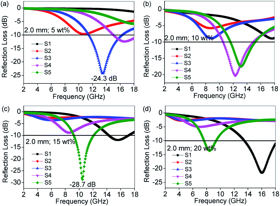 | ||
| Fig. 5 Microwave RL curves of the S1–S5 with loading content of (a) 5 wt%, (b) 10 wt%, (c) 15 wt%, (d) 20 wt% at a thickness of 2.0 mm in the frequency range of 2–18 GHz. | ||
Taking S5 as an example, Fig. 6a shows the reflection loss of S5 under different thicknesses. Furthermore, the 3D image map is displayed in Fig. 6b. Obviously, the RL peaks gradually shift towards lower frequency as the layer thickness increases. This phenomenon can be explained by the quarter-wavelength cancellation model. In this model, when the absorbent reaches the matching thickness (tm) and satisfies the following eqn (3), the phase difference between the entering wave and the emerging wave is 180°, leading to the extinction of the electromagnetic energy at the air–absorber interface.38 From Fig. 6c, it is worth noting that the experimental results are consistent with the quarter-wavelength (λ/4) matching model. Furthermore, the quarter-wavelength matching model also corresponds to the contour map (Fig. 6d).
 | (3) |
 | ||
| Fig. 6 (a) Microwave RL curves, (b) three-dimensional representation, (c) the frequency dependence of matching thickness and calculated thickness tm and (d) two-dimensional representation of the reflection loss values for S5 under different thicknesses in the frequency range of 2–18 GHz. | ||
To investigate the probable mechanism for EM absorption performance, the complex permittivity and permeability of the different composites are analyzed below. Herein, as the octahedral NiS2/NiS nanocrystals are nonmagnetic materials, their μ′ and μ′′ approximate to 1 and 0. Therefore, we only need to focus on the analysis of complex permittivity. Due to the optimal RL value appearing at a filler loading of 5 wt% and 15 wt%, we take 5 wt% and 15 wt% as examples to analyze the variation trend of the real (ε′) and imaginary (ε′′) parts of the relative complex permittivity in 2–18 GHz. Fig. 7 displays the frequency dependence of ε′ and ε′′ with various samples dispersed in PVDF at different mass fractions. It is clearly seen that all the ε′ and ε′′ values increase dramatically after the introduction of RGO, indicating that RGO can improve polarization ability and dielectric-loss capability significantly. Furthermore, all the ε′ curves show a decreasing trend with increasing frequency, which is indicative of a frequency dispersion behavior that can be explained by the increased lagging of polarization with respect to electric-field change at higher frequency.39 This decreasing trend also occurs in the case of ε′′. Another important parameter relating to the polarization loss is called the dielectric loss tangent (tan δε = ε′′/ε′). As shown in Fig. S2,† the dielectric loss value of S2 is higher than other samples, indicating that the RGO in RGO–NiS2/NiS nanocomposites plays a more dominant role in determining the dielectric loss properties. However, the sample with the best absorbing performance is not S2, indicating that there are many other factors which influence the ultimate EM wave absorbing ability.
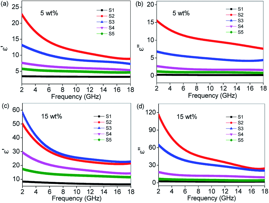 | ||
| Fig. 7 Frequency dependence on (a) real and (b) imaginary parts of the complex permittivity for S1–S5 with a loading content of 5 wt%; frequency dependence on (c) real and (d) imaginary parts of the complex permittivity for S1–S5 with a loading content of 15 wt%. | ||
For RGO–NiS2/NiS nanocomposites, the effective dielectric loss mechanism would be induced by polarization relaxation. In general, the polarization relaxation mainly derives from electron polarization, ion polarization, dipole polarization and space charge polarization. However, in the gigahertz frequency region, the electron and ion polarizations are negligible, the dipole polarization and space charge polarization (i.e. interface polarization) are dominant.40 In this case, the dipoles and interfaces in the samples S2–S5 increase as the RGO proportion and the mass percentage enhances resulting in the growth of ε′ and ε′′. The interfacial polarization usually occurs in materials composed of more than one phase.41 In RGO–NiS2/NiS/PVDF composites, the interface is caused by RGO, NiS2/NiS and PVDF. Moreover, the existing defects and functional groups in RGO are additional two relaxation processes. As is well-known, defects can act as polarization centers, which can generate polarization relaxation under the alternating EM field.42 The electron migration would exist inside these samples when exposed to an electromagnetic field, which leads to electric charge accumulation at the disorder interfaces and defects, acting as a “micro-capacitor”. This could be attributed to the improved impedance matching.43 According to the fundamental mechanism of electromagnetic wave absorption, highly efficient microwave absorbing materials require not only good electromagnetic wave dissipation capability but also impedance matching.44 Ideal impedance matching should satisfy |Zin/Z0| = 1.0, which implies the complete entrance of incident EM wave into an absorber with zero reflection at the air–absorber interface.45 Fig. 8 clearly demonstrates the relationship between RL values and the modulus of normalized input impedance (|Zin/Z0|) for S1–S5 with thicknesses of 1.5 mm and 2.0 mm at a filler loading of 5 wt% and 15 wt%, respectively. It is clearly seen that the minimum reflection loss peaks are basically located at the frequency satisfying the perfect impedance matching (|Zin/Z0| = 1.0), which is another significant influencing factor for strong EM wave dissipation.
 | ||
| Fig. 8 Microwave RL curves of the S1–S5 with loading contents of (a) 5 wt%, (b) 15 wt% at a thickness of 1.5 mm; frequency dependences of relative input impedance (|Zin/Z0|) for S1–S5 with loading contents of (c) 5 wt%, (d) 15 wt%; microwave RL curves of the S1–S5 with loading contents of (e) 5 wt%, (f) 15 wt% at a thickness of 2.0 mm. | ||
To the best of our knowledge, apart from impedance match, another crucial factor in judging the electromagnetic property is attenuation constant (α), which determines the attenuation properties of materials. It can be expressed as:46
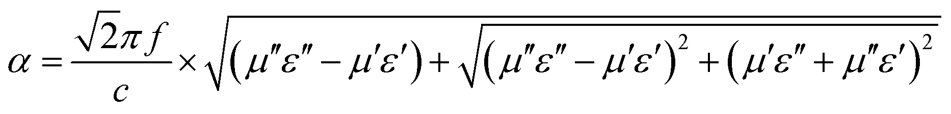 | (4) |
Overall, the excellent EM wave absorption capacity is attributed to the good impedance match, the dielectric loss (caused by dipole polarization, interfacial polarization, defect polarization, etc.), appropriate synergistic effect between RGO, NiS2/NiS nanocrystals and PVDF matrix.
Experimental
Graphite oxide (GO) powder was purchased from Nanjing XFNANO Material Technology Co., Ltd. All other chemicals were of analytical grade and used without further purification.Preparation of octahedral NiS2/NiS nanocrystals
In a typical synthesis, 0.349 g of nickel nitrate hexahydrate (Ni(NO3)2·6H2O) and 0.064 g of sulfur powder were dispersed into 60 mL of ethylene glycol (EG) by stirring for 20 min. Then 0.24 g of polyvinyl pyrrolidone (PVP-40000) was added. After stirring for another 40 min, the homogeneous suspension was transferred into a Teflon-lined stainless-steel autoclave for solvothermal reaction at 200 °C for 12 h, then the solution was cooled to room temperature. The resultant black precipitate of octahedral NiS2/NiS nanocrystals (named as S1) was washed several times with distilled water and absolute ethanol and finally dried at 60 °C for 12 h for further characterization.
Preparation of RGO–NiS2/NiS nanocomposites
With reference to our previous synthesis method,47 to obtain RGO–NiS2/NiS nanocomposites, 40 mg of GO powder was firstly dispersed in 60 mL of water and sonicated for 1 h under ambient conditions. Then the flask was transferred into an oil bath and heated at 90 °C. 40 μL hydrazine hydrate was added to this solution. After 2 h, the GO was chemically reduced to RGO. Finally, 20 mg, 40 mg, 80 mg and 160 mg of octahedral NiS2/NiS nanocrystals were added to the RGO suspension and sonicated for another 2 h, respectively (named as S2, S3, S4 and S5). The resultant black product was isolated by centrifugation, washed with absolute ethanol and finally freeze dried for 12 h.Characterization
XRD analyses were carried out on an X-ray diffractometer (D/MAX-1200, Rigaku Denki Co. Ltd, Japan). The XRD patterns with Cu Kα radiation (λ = 1.5406 Å) at 40 kV and 40 mA were recorded in the range of 2θ = 5°–80°. Scanning electron microscope (SEM) images were achieved by a FEI Quanta 250 field-emission gun environmental scanning electron microscope at 15 kV with the samples obtained from the thick suspension dropping on the silicon slice. Field emission scanning electron microscopy (FE-SEM) on a JSM-6700F microscope. Raman spectra were recorded from 800 cm−1 to 2000 cm−1 on a LabRAM HR800 Laser Raman spectroscopy (HORIBA Jobin Yvon CO. Ltd, France) by using a 632.5 nm argon ion laser. X-ray photon spectroscopy was studied with a Thermo Scientific ESCALAB 250 Xi XPS system.EM absorption measurement
The composites used for EM absorption measurement were prepared by mixing the synthesized octahedral NiS2/NiS nanocrystals with polyvinylidene fluoride (PVDF) in different mass percentages (5 wt%, 10 wt%, 15 wt% and 20 wt%), respectively. The mixtures were then pressed into cylindrical-shaped samples (Φout = 7.00 mm and Φin = 3.04 mm). The complex permittivity and permeability values were measured in the 2–18 GHz range with coaxial wire method by an Agilent N5230C PNA-L Network Analyzer.Conclusions
In summary, RGO–NiS2/NiS nanocomposites with various weight ratios of GO and NiS2/NiS nanocrystals were synthesized by a facile method. Subsequently, the RGO–NiS2/NiS nanocomposites were mixed with PVDF matrix loading different mass fractions (5, 10, 15, 20 wt%) to examine their microwave absorption properties. Both the real and imaginary parts of the permittivity of these hybrids increased with increasing mass fractions of RGO. However, the sample with a GO:NiS2/NiS weight ratio of 1:4 achieves the strongest EM wave absorption. The minimum RL value reaches −32.2 dB at 14.32 GHz and the effective absorption band width covers 4.32 GHz with a thin layer thickness of just 1.5 mm (15 wt%). When the weight ratio increases to 1:1, the minimum RL value changes to −24.3 dB (13.44 GHz) and the effective frequency bandwidth is up to 4.72 GHz with a thickness of 2.0 mm under a filler content of only 5 wt%. The excellent microwave-absorbing behavior is mainly ascribed to dielectric loss (such as dipole polarization, interfacial polarization, defect polarization, etc.), the improved impedance matching and the synergistic effect. This study provides an effective and facile method to produce light-weight absorbers for electromagnetic wave absorbing applications.
Conflicts of interest
There are no conflicts to declare.Acknowledgements
This work was supported by the National Natural Science Foundation of China (51472012) and the Fundamental Research Funds for the Central Universities and China Postdoctoral Science Foundation Grant (2017M620572).Notes and references
- Y. Zhang, Y. Huang, H. Chen, Z. Huang, Y. Yang, P. Xiao, Y. Zhou and Y. Chen, Carbon, 2016, 105, 438–447 CrossRef CAS.
- B. Zhao, X. Guo, Y. Zhou, T. Su, C. Ma and R. Zhang, CrystEngComm, 2017, 19, 2178–2186 RSC.
- Q. Liu, Q. Cao, H. Bi, C. Liang, K. Yuan, W. She, Y. Yang and R. Che, Adv. Mater., 2016, 28, 486–490 CrossRef CAS PubMed.
- N. Zhang, Y. Huang and M. Wang, Composites, Part B, 2018, 136, 135–142 CrossRef CAS.
- H. Xu, X. Yin, M. Zhu, M. Han, Z. Hou, X. Li, L. Zhang and L. Cheng, ACS Appl. Mater. Interfaces, 2017, 9, 6332–6341 CrossRef CAS PubMed.
- Y. Li, R. Liu, X. Pang, X. Zhao, Y. Zhang, G. Qin and X. Zhang, Carbon, 2018, 126, 372–381 CrossRef CAS.
- B. Zhao, X. Guo, W. Zhao, J. Deng, G. Shao, B. Fan, Z. Bai and R. Zhang, ACS Appl. Mater. Interfaces, 2016, 8, 28917–28925 CrossRef CAS PubMed.
- X. Han, X. Tong, X. Liu, A. Chen, X. Wen, N. Yang and X.-Y. Guo, ACS Catal., 2018, 8, 1828–1836 CrossRef CAS.
- M. Zhou, Q. Weng, X. Zhang, X. Wang, Y. Xue, X. Zeng, Y. Bando and D. Golberg, J. Mater. Chem. A, 2017, 5, 4335–4342 RSC.
- G. Xu, X. Wang, Y. Sun, X. Chen, J. Zheng, L. Sun, L. Jiao and J. Li, Nano Res., 2015, 8, 2946–2953 CrossRef CAS.
- Q. Chen, S. Sun, T. Zhai, M. Yang, X. Zhao and H. Xia, Adv. Energy Mater., 2018, 8, 1800054 CrossRef.
- Y. Xiao, D. Su, X. Wang, S. Wu, L. Zhou, Y. Shi, S. Fang, H.-M. Cheng and F. Li, Adv. Energy Mater., 2018, 8, 1800930 CrossRef.
- P. Geng, S. Zheng, H. Tang, R. Zhu, L. Zhang, S. Cao, H. Xue and H. Pang, Adv. Energy Mater., 2018, 8, 1703259 CrossRef.
- G. Zhang, H. Liu, J. Qu and J. Li, Energy Environ. Sci., 2016, 9, 1190–1209 RSC.
- Y. Lu, B. Li, S. Zheng, Y. Xu, H. Xue and H. Pang, Adv. Funct. Mater., 2017, 27, 1703949 CrossRef.
- J. Balamurugan, C. Li, S. G. Peera, N. H. Kim and J. H. Lee, Nanoscale, 2017, 9, 13747–13759 RSC.
- S. Wang, H. Yu, H. Zhang, A. Wang, M. Zhao, Y. Chen, L. Mei and J. Wang, Adv. Mater., 2014, 26, 3538–3544 CrossRef CAS PubMed.
- M. Q. Ning, M. M. Lu, J. B. Li, Z. Chen, Y. K. Dou, C. Z. Wang, F. Rehman, M. S. Cao and H. B. Jin, Nanoscale, 2015, 7, 15734–15740 RSC.
- M. Lu, X. Wang, W. Cao, J. Yuan and M. Cao, Nanotechnology, 2016, 27, 065702 CrossRef PubMed.
- X. Luo, G. S. Wang, H. Y. Guo, X. J. Zhang, W. Q. Cao, Y. Z. Wei, L. Guo and M. S. Cao, ChemPlusChem, 2014, 79, 1089–1095 CrossRef CAS.
- T. Huang, M. He, Y. Zhou, S. Li, B. Ding, W. Pan, S. Huang and Y. Tong, RSC Adv., 2016, 6, 100392–100400 RSC.
- Y. F. Pan, G. S. Wang, L. Liu, L. Guo and S. H. Yu, Nano Res., 2017, 10, 284–294 CrossRef CAS.
- X. J. Zhang, S. W. Wang, G. S. Wang, Z. Li, A. P. Guo, J. Q. Zhu, D. P. Liu and P. G. Yin, RSC Adv., 2017, 7, 22454–22460 RSC.
- L. Wang, Y. Huang, X. Sun, H. Huang, P. Liu, M. Zong and Y. Wang, Nanoscale, 2014, 6, 3157–3164 RSC.
- Y. Zhang, Y. Huang, T. Zhang, H. Chang, P. Xiao, H. Chen, Z. Huang and Y. Chen, Adv. Mater., 2015, 27, 2049–2053 CrossRef CAS.
- B. Wen, X. X. Wang, W. Q. Cao, H. L. Shi, M. M. Lu, G. Wang, H. B. Jin, W. Z. Wang, J. Yuan and M. S. Cao, Nanoscale, 2014, 6, 5754–5761 RSC.
- M. Han, X. Yin, Z. Hou, C. Song, X. Li, L. Zhang and L. Cheng, ACS Appl. Mater. Interfaces, 2017, 9, 11803–11810 CrossRef CAS.
- Q. Zeng, X. H. Xiong, P. Chen, Q. Yu, Q. Wang, R. C. Wang and H. R. Chu, J. Mater. Chem. C, 2016, 4, 10518–10528 RSC.
- C. Zhang, B. Wang, J. Xiang, C. Su, C. Mu, F. Wen and Z. Liu, ACS Appl. Mater. Interfaces, 2017, 9, 28868–28875 CrossRef CAS.
- X. J. Zhang, G. S. Wang, Y. Z. Wei, L. Guo and M. S. Cao, J. Mater. Chem. A, 2013, 1, 12115–12122 RSC.
- A. P. Guo, X. J. Zhang, S. W. Wang, J. Q. Zhu, L. Yang and G. S. Wang, ChemPlusChem, 2016, 81, 1305–1311 CrossRef CAS.
- H. Lv, Y. Guo, Z. Yang, Y. Cheng, L. P. Wang, B. Zhang, Y. Zhao, Z. J. Xu and G. Ji, J. Mater. Chem. C, 2017, 5, 491–512 RSC.
- J. Lv, Y. Cheng, W. Liu, B. Quan, X. Liang, G. Ji and Y. Du, J. Mater. Chem. C, 2018, 6, 1822–1828 RSC.
- T. An, Y. Wang, J. Tang, W. Wei, X. Cui, A. M. Alenizi, L. Zhang and G. Zheng, J. Mater. Chem. A, 2016, 4, 13439–13443 RSC.
- W. Xu, G. S. Wang and P. G. Yin, Carbon, 2018, 139, 759–767 CrossRef CAS.
- C. Tian, Y. Du, P. Xu, R. Qiang, Y. Wang, D. Ding, J. Xue, J. Ma, H. Zhao and X. Han, ACS Appl. Mater. Interfaces, 2015, 7, 20090–20099 CrossRef CAS PubMed.
- S. He, G. S. Wang, C. Lu, J. Liu, B. Wen, H. Liu, L. Guo and M. S. Cao, J. Mater. Chem. A, 2013, 1, 4685–4692 RSC.
- M. Qiao, X. Lei, Y. Ma, L. Tian, X. He, K. Su and Q. Zhang, Nano Res., 2018, 11, 1500–1519 CrossRef CAS.
- H. Wang, Y. Y. Dai, D. Y. Geng, S. Ma, D. Li, J. An, J. He, W. Liu and Z. D. Zhang, Nanoscale, 2015, 7, 17312–17319 RSC.
- H. Lv, Y. Guo, G. Wu, G. Ji, Y. Zhao and Z. J. Xu, ACS Appl. Mater. Interfaces, 2017, 9, 5660–5668 CrossRef CAS PubMed.
- C. Zhou, S. Geng, X. Xu, T. Wang, L. Zhang, X. Tian, F. Yang, H. Yang and Y. Li, Carbon, 2016, 108, 234–241 CrossRef CAS.
- B. Quan, X. Liang, G. Ji, Y. Cheng, W. Liu, J. Ma, Y. Zhang, D. Li and G. Xu, J. Alloys Compd., 2017, 728, 1065–1075 CrossRef CAS.
- T. Zhang, J. Zhang, G. Wen, B. Zhong, L. Xia, X. Huang, H. Zhao, H. Wang and L. Qin, Carbon, 2018, 136, 345–358 CrossRef CAS.
- S. Liu, M. Zhang, X. Lv, Y. Wei, Y. Shi, J. Zhang, L. Zhang and C. Gong, Appl. Phys. Lett., 2018, 113, 083905 CrossRef.
- X. Liu, X. Nie, R. Yu and H. Feng, Chem. Eng. J., 2018, 334, 153–161 CrossRef CAS.
- D. Ding, Y. Wang, X. Li, R. Qiang, P. Xu, W. Chu, X. Han and Y. Du, Carbon, 2017, 111, 722–732 CrossRef CAS.
- X. J. Zhang, G. S. Wang, W. Q. Cao, Y. Z. Wei, J. F. Liang, L. Guo and M. S. Cao, ACS Appl. Mater. Interfaces, 2014, 6, 7471–7478 CrossRef CAS.
Footnotes |
| † Electronic supplementary information (ESI) available. See DOI: 10.1039/c8ra10633a |
| ‡ They are co-first author. |
| This journal is © The Royal Society of Chemistry 2019 |