
 Open Access Article
 This Open Access Article is licensed under a
 Creative Commons Attribution 3.0 Unported Licence
Characterization of contact resistances in ceramic-coated vertically aligned carbon nanotube arrays†
Meng Li a,
Ning Yanga,
Vanessa Wood*b and
Hyung Gyu Park‡
*a
a,
Ning Yanga,
Vanessa Wood*b and
Hyung Gyu Park‡
*a
aDepartment of Mechanical and Process Engineering, ETH Zürich, Zürich CH-8092, Switzerland. E-mail: parkh@ethz.ch
bDepartment of Information Technology and Electrical Engineering, ETH Zürich, Zürich CH-8092, Switzerland. E-mail: vwood@ethz.ch
First published on 4th March 2019
Abstract
Despite the technological significance of carbon nanotube (CNT) arrays and metal-oxide coated CNTs for electronic and electrochemical devices such as supercapacitors, lithium-ion batteries, and solar-chemical cells, sub-optimal device performance often results due to large contact resistance between the CNTs and the metallic current collectors or between the CNTs and their ceramic coatings. While contact resistance measurements are regularly carried out on individually contacted CNTs, contact resistance measurements on vertically aligned (VA) CNT arrays are not routine. Here, we demonstrate that two-probe electrical current–voltage measurements and electrochemical impedance spectroscopy can be used to probe the end contact resistance and side contact resistances of coated and uncoated VACNT arrays in order to optimize material deposition and selection.
1. Introduction
With highly directional transport and a large graphitic surface area for functionalization, vertically aligned carbon nanotube (CNT) arrays have outstanding electrical and physical properties1–3 for a number of different types of devices.4 For instance, it has been predicted that a densely packed forest of vertically aligned CNTs (VACNTs) could outperform Cu as microelectronic interconnects.5 CNTs decorated with conductive polymers or inorganic oxides have applications in electrochemical devices such as supercapacitors,6,7 dye-sensitized solar cells,8 and water splitting cells.9 Used as a conductive additive, CNTs help lower electrode resistance to enhance capacitive deionization performance for salt water desalination,10 or increase the rate performance and cyclability in lithium-ion batteries.11 Given the low bulk resistance of the CNTs, the contact resistance they form at the interface with charge collectors or surface coatings play a critical role in the overall device performance.In order to minimize ohmic losses, it is necessary for the CNTs to be electrically connected with minimal resistance to the charge collectors and for coatings to be electrically connected with minimal resistance to the CNTs. Although a theoretical quantum contact resistance of a single-walled carbon nanotube (SWCNT) is ∼6.45 kΩ,12 experimentally measured contact resistances span many orders of magnitude.13,14 For multi-walled CNTs (MWCNTs), contact resistance variations can be even greater. For example, a MWCNT (∼100 nm in diameter) semi-spherically coated with Ti/Au over a large contact area, contact resistance (Rc) has been reported to be 1.56 kΩ.15 However, a resistance value of ∼1 GΩ has been reported for the case where the tube is placed directly on small, pre-deposited Au finger electrodes without any further treatment.16 Reasons for these large discrepancies (in addition to differences in the CNTs themselves) include differences in contact area and configuration (side- or end contact), physio-chemical parameters of the contact (e.g., work function and wettability),17 and the type of interfacial contact (e.g., quantum mechanical tunneling18–20 vs. classical Schottky junction21,22).
Most reports13–16,23–30 measure the Rc of a suspended CNT, which involves use of advanced nanofabrication and characterization such as in situ transmission electron microscopy (TEM) or conductive atomic force microscopy (AFM). Although quite precise, these methods are usually costly and time-consuming. On a device scale, the ensemble-averaged, end-contact resistance per nanotube can be obtained from a polished VACNT forest less than a micrometer in height.17,31,32 This approach loses accuracy the taller the CNT forest (tall CNT forests offer higher mass loading in electrochemical devices33) because their lengths become the more heterogeneous.34,35
Here, we establish characterization methods for both side- and end-contact resistances of VACNT forests (Fig. 1). We show that two-probe electrical measurements can be used to determine contact resistances between the end of the CNTs and the current collector. It is further possible to determine the effective spacing between the metallic current collector and the CNTs, which relates to the electronic structure of the substrate and the wetting of the metal and the CNTs. To determine side contact resistances between a coating and a CNT sample, we show that electrochemical techniques (cyclic voltammetry and electrochemical impedance spectroscopy) enable the decoupling of impedance contributions from different origins. Combined with knowledge of the average length and number of CNTs in the array, the resistivity of the coating itself can also be determined.
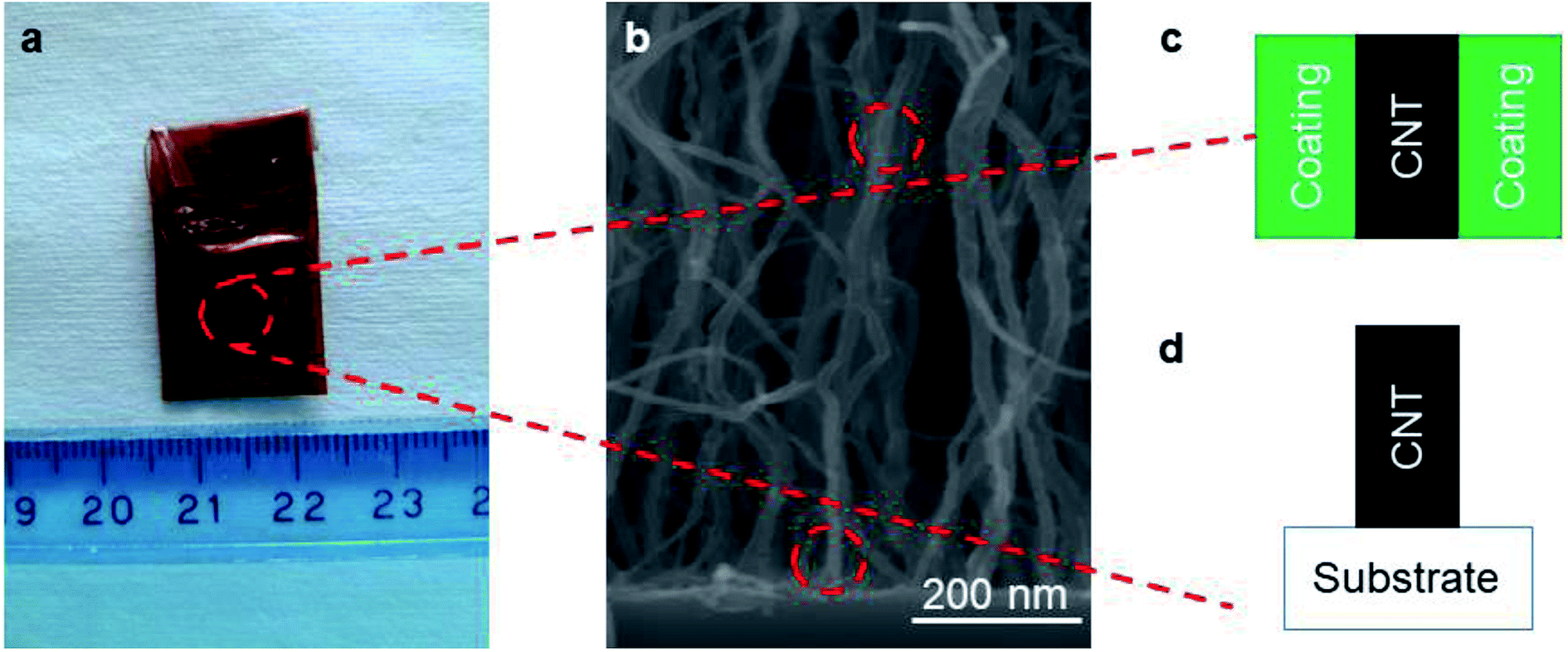 | ||
| Fig. 1 (a) Photograph of a typical TiO2/VACNT electrode, (b) SEM image of TiO2-coated VACNTs. Schematics of (c) side contact between CNT side wall and oxide coating and (d) end contact between CNT bottom end and current collector. | ||
2. Experimental
2.1 Material synthesis
To grow a VACNT array, a catalyst layer consisting of a (nominal) 3 nm-thick Fe layer atop a 20 nm-thick Al barrier film was deposited via e-beam evaporation on Si chips (0.5 mm in thickness) or on Ni foils (Alfa Aesar, 99% metal basis, 0.025 mm in thickness). Prior to the catalyst deposition, the Ni foil surface was physically etched away with mild Ar+ beam milling in order to remove contaminants. The catalyst samples were loaded into a quartz tube furnace, heated up to 750 °C at 30 °C min−1 at ambient pressure with a flow of 600 sccm of H2 and 400 sccm of Ar, and annealing for 20 min at these conditions. After annealing, C2H4 (250 sccm) was added to the gas ambient to grow VACNT forests. TiO2 was coated on the as-grown VACNTs via plasma-enhanced atomic layer deposition (ALD) at 120 °C in an Oxford Instrument AL1 FlexAL system. Each cycle consisted of a 1.5 s dose (at 200 sccm) of Tetrakis(dimethylamino)titanium as a Ti precursor and a 10 s dose (at 20 sccm) of ozone plasma as an oxygen source.2.2 VACNT transplantation
VACNT transplantation was done via a poly(methyl methacrylate) (PMMA) assisted stamping procedure described previously.8 The as-grown CNT samples were pressed into a coating (∼1 μm in thickness) of PMMA on different conductive substrates, i.e. FTO glass, W coated glass or Ni foil, before curing and peeling off. The PMMA layer was then pyrolized by annealing in 900 sccm H2/100 sccm Ar at 400 °C for 2 h. The pyrolysis process removes most of the PMMA,36 and thus does not interfere with the electrical or weight measurements. The transferred CNTs were weighed on a new substrate with a Mettler Toledo XP2U ultra-micro balance (1 μg in resolution) before and after transplantation.2.3 Characterizations
The height and alignment of the VACNTs were characterized using scanning electron microscopes (SEM, FEI Nova 450 and Hitachi SU 8200). TEM was used to obtain CNT diameter statistics (Philips CM12). Catalyst particle density was probed with a Bruker Fastscan AFM. The as-grown CNT quality and the phase information of the as-deposited TiO2 layer were determined by use of a Renishaw InVia Raman spectroscope (785 nm excitation) and NTMDT NTEGRA Raman spectroscope (571 nm excitation).3. Results and discussion
3.1 VACNTs characterization
To perform macroscopic measurement on a VACNT array and then extract information about the average properties of individual tubes, we first need to know the properties of the CNTs, including their areal number density (nCNT), length (l), and linear resistivity (ρ′′). Literature has shown that the linear resistivity relies heavily on the CNT quality, such as wall number (n), diameter and defect density,37,38 and is usually described by a charge mean-free-path theory.14,39Fig. 2 provides information about the VACNT forests investigated in this work. As can be seen from Fig. 2c and d, the VACNTs near the top of the forest are more aligned, while they are less dense and more entangled near the bottom, consistent with a density decay regime.40,41 After transplantation (where the “top” and “bottom” end of the CNTs are reversed), both the forest height (L) and alignment are well preserved with minimal bending at the top likely caused by decreased CNT number density or small pressures applied during the transfer process. Statistics over 300 tubes grown in different batches reveal that the MWCNTs possess an average outer diameter (dout) of 10.2 ± 0.42 nm and inner diameter (din) of 6.0 ± 0.47 nm (more details can be found in Fig. S1†). With ∼0.34 nm as the interlayer spacing between CNT walls,42 an averaged n of each CNT is estimated as ∼6. Raman spectra at the top and bottom of a CNT forest are similar with unchanged Raman D-to-G intensity ratio (∼1.35) along the thickness, suggesting an invariant defect density as well as ρ′′ along the CNTs.37 We note that the bottom end switches with the top after transplantation. Regardless of the growth time (t) or forest height, CNTs remain of similar characteristics in terms of tube diameter and quality (information about VACNTs of other thicknesses can be found in Fig. S1†).
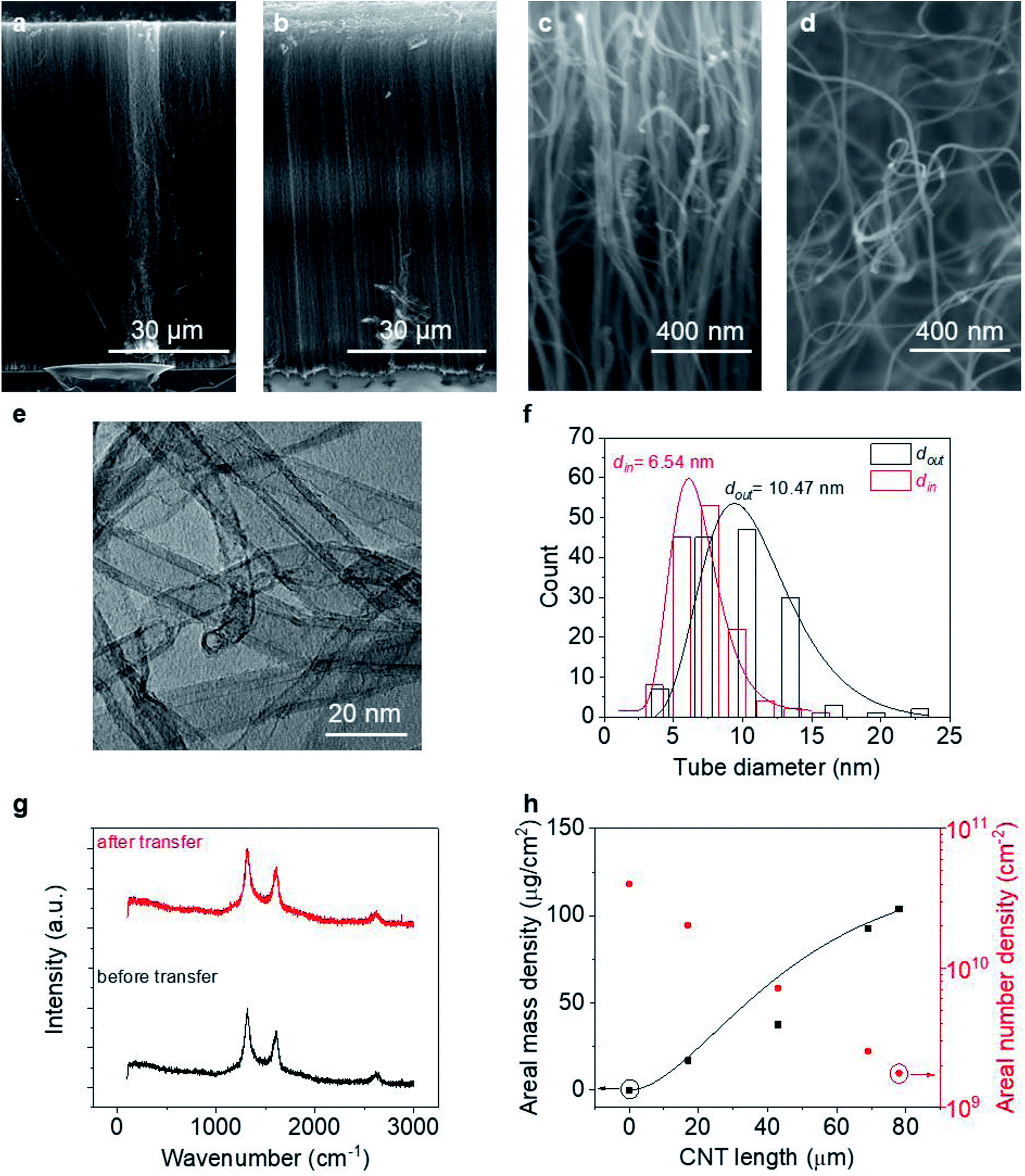 | ||
| Fig. 2 CNT characteristics: SEM images of the VACNT forest before (a) and after transplantation (b). High magnification images near the top (c) and bottom (d) of the forest, prior to transplantation; (e) typical TEM image of CNTs (f) inner and outer diameter statistics; (g) Raman spectra of CNTs before and after transfer. (h) Areal mass and number density of CNTs in VACNT forest. | ||
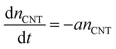
Counting the number of CNTs from cross-sectional SEM images alone may not provide an accurate effective nCNT because an SEM of a porous structure like a CNT forest contains depth information. A more accurate and reliable way is the weight-gain method,43 which allows us to describe nCNT and model its dependency on L. Assuming the tube growth is self-terminated44 with a catalyst deactivation probability constant a, one can relate areal density nCNT to growth time t:
 | (1) |
Neglecting the initial CNT self-organization period, nCNT roughly equals to the catalyst number density (N0 = 4 × 1010 cm−2 from AFM data, Fig. S2†) at t = 0. Integration over eqn (1) gives:
nCNT = N0![[thin space (1/6-em)]](https://www.rsc.org/images/entities/char_2009.gif) exp(−at) exp(−at)
| (2) |
The mass of the entire VACNT forest (M) over area (A) can then be written as the summation of all the nanotubes grown until t:
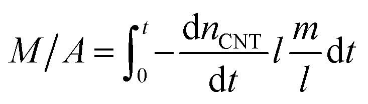 | (3) |
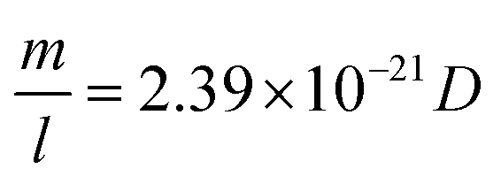
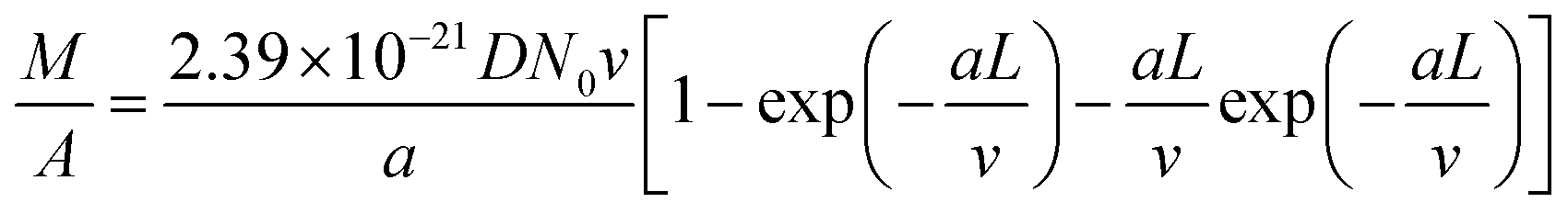
In this equation, m (in g) and l (in nm) are the mass and length of an individual tube at t. To proceed, two maneuvers can be applied. One is to set l = vt, where v is the steady-state growth rate of the VACNT forest (10 μm min−1 in this study). Another is to consider the specific surface area of a MWCNT referring to the literature43 (eqn (4)), where D is the aggregate diameter of all the carbon walls summed up (53 ± 2.5 nm from our TEM analysis):
 | (4) |
Combining eqn (1)–(4) and replacing the final t with L/v, we finally reach:
 | (5) |
Fitting Fig. 2h with eqn (5) (black line) yields a = 0.40 min−1. Plugging this value to eqn (2), we can see that nCNT drops by a factor of ∼20 when L becomes longer than ∼80 μm. The relatively short length (submillimeter) and low density (O(≤1010) cm−2) agree with previous findings in the literature that the growth of the VACNT forest is limited by catalyst poisoning.45 Extrapolation of eqn (5) predicts saturation of the CNT forest growth if L exceeds 150 μm (M/A reaching a plateau, and entering the termination stage40), which is in good agreement with our experimental data.
3.2 Measuring end contact resistance of VACNTs
To determine the end contact resistance, we use the two-probe electrical current–voltage measurements shown in Fig. 3a. The measurements are carried out with a probe station (Cascade) connected to a semiconductor device analyzer (Agilent B1500A). A pair of W probes (19 μm in diameter, giving Aprobe = 2.83 × 10⁻⁶ cm2) is aligned horizontally with a separation distance of ∼100–200 μm and then carefully placed atop the CNT forest (approaching in 2 μm steps) to make direct electrical contact. Measurements are repeated at a minimum of 6 distinct positions on each sample.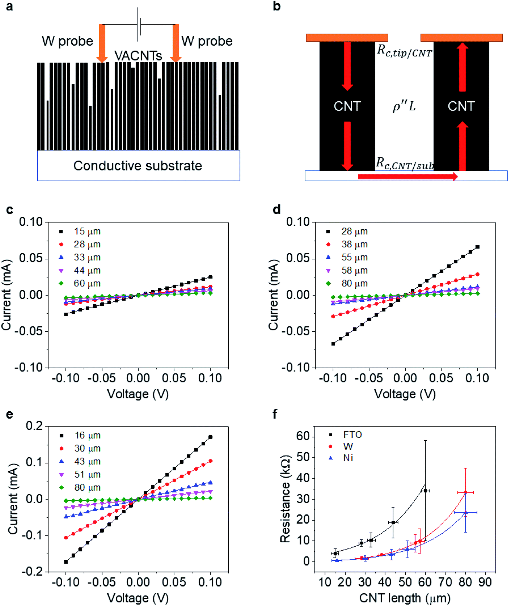 | ||
| Fig. 3 Measurements of VACNT end contact resistance: schematics (a) of the I–V test setup and (b) measurement with red arrows marking the electron flow; typical I–V curves of as-transplanted VACNTs in different length on (c) FTO, (d) W and (e) Ni substrates; and (f) plot of resistance versus CNT length for CNTs on FTO, W, and Ni. | ||
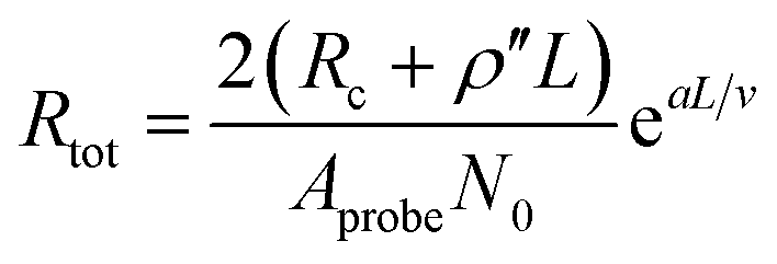
When using this setup, electrons are injected from one W probe into multiple CNTs (about ∼ 104) in parallel. CNTs much shorter than the average are not probed. As reported previously,32 the lateral resistance between CNTs in the VACNT forest is large enough to neglect. Most injected electrons thus travel across the bottom conductive substrate and exit from CNTs that contact another probe (Fig. 3b). Therefore, one can write the resistance (R) per individual CNT as:
| R = AprobenCNTRtot/2 = Rc,tip-CNT + ρ′′L + Rc,CNT-sub | (6) |
Fig. 3c–e shows the I–V curves of as-transplanted VACNTs on various substrates. For any given VACNT height and bottom contact, a linear I–V curve is observed so Rtot is the inverse slope. Plotting Rtot vs. the VACNT height shows a non-linear behavior (Fig. 3f). As discussed previously, while CNT quality (mainly ρ′′ and n) does not vary over l or L, nCNT changes significantly. Therefore, to extract the contact resistance Rc, we combine eqn (2) and (6):
 | (7) |
The fitting results (Table 1) indicate a ρ′′ (∼1.15 MΩ μm−1) and a that are invariant with substrate material. This highlights the reliability of the fit since ρ′′ and a should indeed be intrinsic properties of the CNTs. The fitted values of a match reasonably well with the one from our modified weight-gain approach. At a small electric field, it is very unlikely that optical phonons and zone-boundary phonons play any significant role in electron transport,39 and therefore ρ′′ is dominated by acoustic phonons from scattering at the defects. The ρ′′ value of our MWCNTs is higher than the values measured by dipping a freestanding nanotube into liquid metals2,25,48 (200 Ω μm−1) or in a FET configuration (41 kΩ μm−1),49 but it is quite close to the values measured where the tube is curved by an AFM tip (1.93 MΩ μm−1)50 or under direct probing (1.39 MΩ μm−1).51 This finding suggests that in addition to the CNT quality, ρ′′ might also be sensitive to slight bending (Fig. 2b). In fact, theoretical modelling has shown that the resistance of CNT under mechanical deformation can change.52
| Substrate material | EF (eV) | Rc (MΩ) | ρ′′ (MΩ μm−1) | a (min−1) | Gap distance (Å) |
|---|---|---|---|---|---|
| FTO | 5.0 | 125.2 | 1.2 | 0.4 | 5.9 |
| W | 4.55 | 1.28 | 1.14 | 0.34 | 3.7 |
| Ni | 5.15 | 0.4 | 1.11 | 0.38 | — |
However, Rc varies by orders of magnitudes for the different substrates (Ni, W, and FTO). On Ni, the contact resistance is the lowest with Rc = 0.4 MΩ. Metals with unfilled d-orbitals (Ni has electron configuration 3d84s2) have a strong affinity to carbon atoms53 and can potentially form carbides (covalent bonds) upon annealing. Experiments29,54 have shown that such carbide formation is particularly helpful to obtain a low resistance ohmic contact. Since it is the theoretical quantum resistance for a SWCNT is 6.45 kΩ (ref. 12) and multiple conduction pathways (∼2 for our MWCNT), we expect Ni-MWCNT contact, Rc,CNT-sub, to small enough to be omitted. We can assign the 0.4 MΩ to the contact resistance between the W probes and the VACNT forest (Rc,tip-CNT). This allows us to decouple the Rc,CNT-sub from Rc,tip-CNT for the case of W or FTO substrates.
The value of Rc,CNT-sub for FTO (125.2–0.4 = 124.8 MΩ) is larger than that for W (1.28–0.4 = 0.88 MΩ), which can be attributable to a lack of d vacancies in FTO53 and the relatively weaker carbon affinity to 5d vacancies in W.17 In such a case, the weak bonding is partially van der Waals in nature and can be thought of as an average bonding length (or vacuum gap) of s (in Å) through which electron tunneling occurs.19 At small electrical bias (in our case V ≤ 0.1 V), Simmons55 has derived eqn (8) for electron tunneling between two dissimilar electrodes, in which φ (in eV) is the averaged work function, and J the current density (in A cm−2):
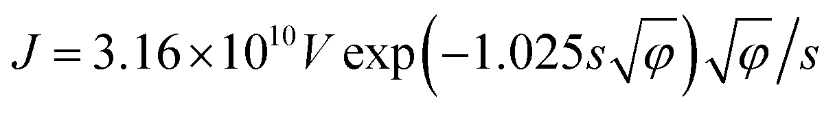 | (8) |
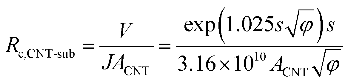 | (9) |
Since both φ and s appear in the exponent, the resistance can differ substantially by the choice of metal leads, consistent with our findings (Table 1). Fitting by eqn (9) gives a tunneling gap of ∼3.7 Å in W and ∼5.9 Å in FTO. In Fig. S3,† we see that as-transplanted CNTs on the FTO substrate detach easily after soaking into water, in contrast to their stability on Ni. This observation supports the fact that CNT bond less strongly to FTO. In short, in order to minimize Rc, it is crucial to have good wetting and to shorten the tunneling gap spacing with metals such as Ti,15,26,56,57 Ni,49,58 and Pd.30
3.3 Measuring side contact resistance of coated VACNTs
To probe the side-contact resistance between a CNT and a coating, we propose electrochemical characterization. We are faced with the geometry shown in Fig. 4a and wish to extract the interface resistance Ri and normalize it with the areal coverage of the coating Acoat to obtain the 2D resistance R2D. To do so, we use electrochemical impedance spectroscopy (EIS) and cyclic voltammetry (CV). By performing these measurements on a series of coated VACNT samples, where the thickness of the coating varies, we are also able to extract the resistance of the coated layer, Rs, and its resistivity, ρcoating.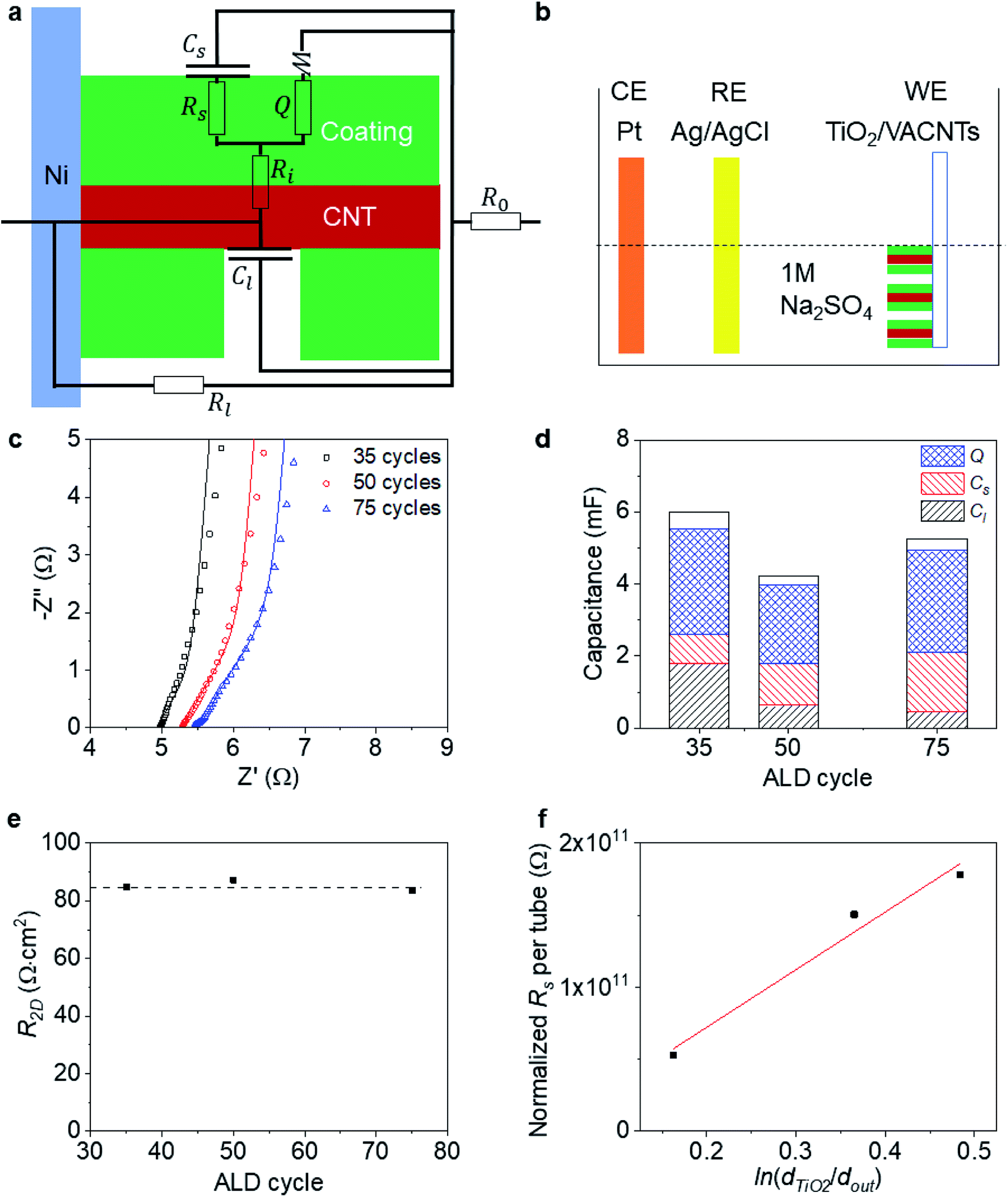 | ||
| Fig. 4 Measurements of VACNT side contact resistance: (a) schematic of a partially TiO2-coated CNT and its equivalent circuit diagram; (b) schematic of the EIS test setup; (c) Nyquist spectra of TiO2/VACNT samples; (d) bar plot of capacitance contributions of TiO2/VACNT samples, with the total capacitance from CV shown with the blank bar; (e) 2D resistance at the interface of TiO2 and CNT for numbers of ALD cycles; and (f) normalized electrical resistance of TiO2 per tube with respect to coating thickness and tube diameter. | ||
To carry out the electrochemical characterization, we use the setup sketched in Fig. 4b. The working electrode consists of either coated or uncoated VACNT samples, which are grown on Ni foil. The samples are partially taped with Kapton, leaving an effective area (Aelectrode) of approximately 0.8 cm × 0.8 cm exposed (see Fig. 1a). This working electrode (WE) is immersed in 1 M Na2SO4 aqueous electrolyte with Pt and Ag/AgCl as counter (CE) and reference electrodes (RE), respectively. We use an electrochemical workstation (CH Instruments, CHI 660E). All measurements are conducted at room temperature.
To demonstrate our approach, we perform electrochemical characterization on three VACNT samples, coated with different thickness layers of TiO2 (35, 50 and 75 cycles) using atomic layer deposition (ALD). The EIS data is acquired at open circuit potential with an oscillation amplitude of 5 mV and shown in Fig. 4c. Previous work has shown that this ALD-based, TiO2 coating bonds covalently onto the MWCNT exterior (L ≈ 100 μm over dout ≈ 10 nm) and forms a side contact as shown schematically in Fig. 4a.59,60 In the first 20 ALD cycles, it is seen that the TiO2 coating grows at a slower rate than at a later stage, which likely comes from inhomogeneous nucleation and growth (Fig. S4†). Therefore, for the relative low numbers of ALD cycles here, we assume that we will not have complete coverage of the TiO2 coating, and include a leakage capacitance Cl (associated with ion adsorption directly onto and off of the CNTs) in the equivalent circuit model used to fit the EIS data (inset of Fig. 4c).
We note that this equivalent circuit model is similar to that of a ref. 61 for a suspended SWCNT coated with MnO2. We assume that the resistance of the CNT is negligible and that we do not observe strong ionic diffusion limitations within the electrolyte (Fig. S5†). In addition to the leakage capacitance Cl, the other parameters in the equivalent circuit model include: the series resistance of the electrode and electrolyte, R0; the leakage resistance to the Ni foil substrate, Rl; the electrical resistance of the TiO2, Rs; the surface capacitance of the TiO2 coating Cs (associated with ion adsorption directly onto and off of the TiO2); the bulk faradaic contribution Q (with non-ideality factor n close to 1), and the Warburg diffusion resistance, W (associated with ionic diffusion into the TiO2); and finally, the key parameter of interest, the interfacial resistance between the CNT and TiO2 coating, Ri.
Values for all fits are provided and trends with number of ALD layers are discussed in the ESI.† To further confirm that the values extracted from the equivalent circuit model fitting to EIS are sensible, we show in Fig. 4d that the sum of all the capacitances (Cl, Cs, and Q) extracted from the equivalent circuit model fitting to EIS are within 8% of the values of the capacitance C extracted from CV measurements (at 100 mV s−1 scanning rate) on the three coated VACNT samples within a 0–0.8 V voltage window.
To determine the 2D interfacial contact resistance R2D from the interfacial resistance Ri, we need to know how much of the CNT surface is coated (Acoat):
| R2D = RiAcoat | (10) |
We use the CV scan to quantify the surface coverage of the coating Acoat. The ratio of the leakage capacitance of the coated-VACNTs (extracted from the EIS measurements) to the capacitance of the uncoated-VACNTs (measured with CV to be C0 ≈ 2.47 mF) enables us to quantify the surface coverage of the coating Acoat using the expression:
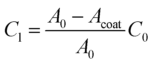 | (11) |
Additionally, we show that the resistivity of the coating, ρTiO2, can be obtained from Rs, extracted from the EIS fitting. This value is important to know because of the type and quality (i.e., crystal phase and morphology) of the coating grown on a high aspect ratio may differ from that grown using the same conditions on a flat 2D substrate. Indeed, here, we show from Raman spectroscopy, that the as-deposited TiO2 is a mixture of anatase and rutile phases (Fig. S4e†). We take the coated CNT to be analogous to a co-axial cable (eqn (12)), where the resistivity of the coating layer takes the form:
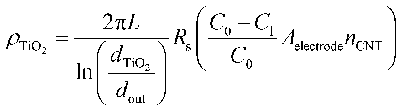 | (12) |
4. Conclusion
In order to systematically design lower resistance electrical and electrochemical devices using CNTs, we present approaches to measure the end contact resistance of CNTs in a VACNT array and the side contact resistances of ceramic coated CNTs in a VACNT array. These approaches can be performed on as-fabricated VACNT arrays or also on arrays that have been transplanted to different substrates. The approaches enable us to determine additional information such as the tunnel distance between the CNTs and the substrate as well as the quality of the coating (i.e., its resistivity).Our study highlights that contact resistances depend on the contact quality, which will be determined by the electronic structure of the substrate or coating material and its wettability with carbon (defining the tunneling barrier). While it is widely known that low-resistance end contacts are found between CNTs and metallic catalysts17,32,34,35,51,66–69 (e.g., a bond as strong as 7.6 eV per bond could be formed between Co catalyst and SWCNT70), our results show that transplantation of CNTs (e.g., on Ni at 400 °C) can still enable low resistively end contacts much below the typical CVD temperature (750 °C). These findings highlight that VACNT arrays can be transferred to substrates and devices on which direct CVD growth of the CNTs is not possible (e.g. flexible substrates, glass) such that their good electrical properties are maintained. However, even a substrate or coating that itself has high quality (e.g., our ALD-coated TiO2 exhibits a low number of defects) may exhibit high contact resistance with the CNTs due, for example, to sub-optimal wetting.
Conflicts of interests
There are no conflicts to declare.Acknowledgements
A large part of this work has been carried out at Binnig Rohrer Nanotechnology Center of ETH Zürich and IBM Zürich. This work was funded by Swiss National Science Foundation through the Sinergia project (contract: CRSII2-147615/1) and the NRP70 Program “Energy Turnaround” (contract: 407040_153978). We also acknowledge the SCCER Heat & Electricity Storage in collaboration with the CTI Energy Programme for provision of a forum for discussion. M. L. is grateful to Prof. Gisbert Schneider at ETH Zurich for allowing him to use an ultra-micro balance.References
- D. Tasis, N. Tagmatarchis, A. Bianco and M. Prato, Chem. Rev., 2006, 106, 1105–1136 CrossRef CAS PubMed.
- P. Poncharal, C. Berger, Y. Yi, Z. Wang and W. A. de Heer, J. Phys. Chem. B, 2002, 106, 12104–12118 CrossRef CAS.
- T. Dürkop, S. Getty, E. Cobas and M. Fuhrer, Nano Lett., 2004, 4, 35–39 CrossRef.
- M. F. De Volder, S. H. Tawfick, R. H. Baughman and A. J. Hart, Science, 2013, 339, 535–539 CrossRef CAS PubMed.
- J. Robertson, G. Zhong, S. Esconjauregui, C. Zhang and S. Hofmann, Microelectron. Eng., 2013, 107, 210–218 CrossRef CAS.
- V. Gupta and N. Miura, Electrochim. Acta, 2006, 52, 1721–1726 CrossRef CAS.
- Z. Fan, J. Chen, B. Zhang, B. Liu, X. Zhong and Y. Kuang, Diamond Relat. Mater., 2008, 17, 1943–1948 CrossRef CAS.
- N. Yazdani, D. Bozyigit, I. Utke, J. Buchheim, S. K. Youn, J. r. Patscheider, V. Wood and H. G. Park, ACS Appl. Mater. Interfaces, 2014, 6, 1389–1393 CrossRef CAS PubMed.
- M. Gong, Y. Li, H. Wang, Y. Liang, J. Z. Wu, J. Zhou, J. Wang, T. Regier, F. Wei and H. Dai, J. Am. Chem. Soc., 2013, 135, 8452–8455 CrossRef CAS PubMed.
- M. Li and H. G. Park, ACS Appl. Mater. Interfaces, 2018, 10, 2442–2450 CrossRef CAS PubMed.
- X.-M. Liu, Z. dong Huang, S. woon Oh, B. Zhang, P.-C. Ma, M. M. Yuen and J.-K. Kim, Compos. Sci. Technol., 2012, 72, 121–144 CrossRef CAS.
- S. Datta, Electronic transport in mesoscopic systems, Cambridge University Press, 1997 Search PubMed.
- A. Bezryadin, A. Verschueren, S. Tans and C. Dekker, Phys. Rev. Lett., 1998, 80, 4036 CrossRef CAS.
- M. S. Purewal, B. H. Hong, A. Ravi, B. Chandra, J. Hone and P. Kim, Phys. Rev. Lett., 2007, 98, 186808 CrossRef PubMed.
- C. Lan, P. Srisungsitthisunti, P. B. Amama, T. S. Fisher, X. Xu and R. G. Reifenberger, Nanotechnology, 2008, 19, 125703 CrossRef PubMed.
- A. Bachtold, M. Henny, C. Terrier, C. Strunk, C. Schönenberger, J.-P. Salvetat, J.-M. Bonard and L. Forro, Appl. Phys. Lett., 1998, 73, 274–276 CrossRef CAS.
- S. C. Lim, J. H. Jang, D. J. Bae, G. H. Han, S. Lee, I.-S. Yeo and Y. H. Lee, Appl. Phys. Lett., 2009, 95, 264103 CrossRef.
- Y. Matsuda, W.-Q. Deng and W. A. Goddard, J. Phys. Chem. C, 2007, 111, 11113–11116 CrossRef CAS.
- T. Yamada, T. Saito, M. Suzuki, P. Wilhite, X. Sun, N. Akhavantafti, D. Fabris and C. Y. Yang, J. Appl. Phys., 2010, 107, 044304 CrossRef.
- Y. Matsuda, W.-Q. Deng and W. A. Goddard III, J. Phys. Chem. C, 2010, 114, 17845–17850 CrossRef CAS.
- J. Svensson and E. E. Campbell, J. Appl. Phys., 2011, 110, 111101 CrossRef.
- Z. Chen, J. Appenzeller, J. Knoch, Y.-m. Lin and P. Avouris, Nano Lett., 2005, 5, 1497–1502 CrossRef CAS PubMed.
- R. Martel, T. Schmidt, H. Shea, T. Hertel and P. Avouris, Appl. Phys. Lett., 1998, 73, 2447–2449 CrossRef CAS.
- S. J. Tans, A. R. Verschueren and C. Dekker, Nature, 1998, 393, 49–52 CrossRef CAS.
- S. Frank, P. Poncharal, Z. Wang and W. A. de Heer, Science, 1998, 280, 1744–1746 CrossRef CAS PubMed.
- J.-O. Lee, C. Park, J.-J. Kim, J. Kim, J. W. Park and K.-H. Yoo, J. Phys. D: Appl. Phys., 2000, 33, 1953 CrossRef CAS.
- P. De Pablo, M. Martınez, J. Colchero, J. Gomez-Herrero, W. Maser, A. De Benito, E. Munoz and A. Baro, Mater. Sci. Eng., C, 2001, 15, 149–151 CrossRef.
- M. Dominiczak, L. Otubo, D. Alamarguy, F. Houzé, S. Volz, S. Noël and J. Bai, Nanoscale Res. Lett., 2011, 6, 1–10 CrossRef PubMed.
- Q. Cao, S.-J. Han, J. Tersoff, A. D. Franklin, Y. Zhu, Z. Zhang, G. S. Tulevski, J. Tang and W. Haensch, Science, 2015, 350, 68–72 CrossRef CAS PubMed.
- A. D. Franklin, D. B. Farmer and W. Haensch, ACS Nano, 2014, 8, 7333–7339 CrossRef CAS PubMed.
- N. Chiodarelli, K. Kellens, D. J. Cott, N. Peys, K. Arstila, M. Heyns, S. De Gendt, G. Groeseneken and P. M. Vereecken, J. Electrochem. Soc., 2010, 157, K211–K217 CrossRef CAS.
- T. Saito, M. Wada, A. Isobayashi, Y. Yamazaki, M. Katagiri, M. Kitamura, B. Ito, T. Matsumoto, N. Sakuma and A. Kajita, Jpn. J. Appl. Phys., 2012, 51, 05ED01 CrossRef.
- P. Simon and Y. Gogotsi, Nat. Mater., 2008, 7, 845–854 CrossRef CAS PubMed.
- Y. Jiang, P. Wang and L. Lin, Nanotechnology, 2011, 22, 365704 CrossRef PubMed.
- T. Vo, C. Poulain, J. Dijon, A. Fournier, N. Chevalier and D. Mariolle, J. Appl. Phys., 2012, 112, 044901 CrossRef.
- F. A. Lehmann and G. M. Brauer, Anal. Chem., 1961, 33, 673–676 CrossRef CAS.
- S. Agrawal, M. Raghuveer, H. Li and G. Ramanath, Appl. Phys. Lett., 2007, 90, 193104 CrossRef.
- G. Chen, D. N. Futaba, S. Sakurai, M. Yumura and K. Hata, Carbon, 2014, 67, 318–325 CrossRef CAS.
- J.-Y. Park, S. Rosenblatt, Y. Yaish, V. Sazonova, H. Üstünel, S. Braig, T. Arias, P. W. Brouwer and P. L. McEuen, Nano Lett., 2004, 4, 517–520 CrossRef CAS.
- M. Bedewy, E. R. Meshot, H. Guo, E. A. Verploegen, W. Lu and A. J. Hart, J. Phys. Chem. C, 2009, 113, 20576–20582 CrossRef CAS.
- M. Bedewy, E. R. Meshot, M. J. Reinker and A. J. Hart, ACS Nano, 2011, 5, 8974–8989 CrossRef CAS PubMed.
- Y. Saito, T. Yoshikawa, S. Bandow, M. Tomita and T. Hayashi, Phys. Rev. B, 1993, 48, 1907–1909 CrossRef CAS.
- S. Esconjauregui, R. Xie, M. Fouquet, R. Cartwright, D. Hardeman, J. Yang and J. Robertson, J. Appl. Phys., 2013, 113, 144309 CrossRef.
- G. G. Tibbetts, J. Cryst. Growth, 1985, 73, 431–438 CrossRef CAS.
- R. Xiang, Z. Yang, Q. Zhang, G. Luo, W. Qian, F. Wei, M. Kadowaki, E. Einarsson and S. Maruyama, J. Phys. Chem. C, 2008, 112, 4892–4896 CrossRef CAS.
- H. B. Michaelson, J. Appl. Phys., 1977, 48, 4729–4733 CrossRef CAS.
- M. Helander, M. Greiner, Z. Wang, W. Tang and Z. Lu, J. Vac. Sci. Technol., A, 2011, 29, 011019 CrossRef.
- C. Berger, Y. Yi, Z. Wang and W. De Heer, Appl. Phys. A: Mater. Sci. Process., 2002, 74, 363–365 CrossRef CAS.
- M. Liebau, E. Unger, G. Duesberg, A. Graham, R. Seidel, F. Kreupl and W. Hoenlein, Appl. Phys. A: Mater. Sci. Process., 2003, 77, 731–734 CrossRef CAS.
- H. Dai, E. W. Wong and C. M. Lieber, Science, 1996, 272, 523–526 CrossRef CAS.
- S. Masahito, Y. Kashiwagi, Y. Li, K. Arstila, O. Richard, D. J. Cott, M. Heyns, S. De Gendt, G. Groeseneken and P. M. Vereecken, Nanotechnology, 2011, 22, 085302 CrossRef PubMed.
- M. B. Nardelli and J. Bernholc, Phys. Rev. B, 1999, 60, R16338 CrossRef CAS.
- Y. Zhang, N. W. Franklin, R. J. Chen and H. Dai, Chem. Phys. Lett., 2000, 331, 35–41 CrossRef CAS.
- Y. Zhang, T. Ichihashi, E. Landree, F. Nihey and S. Iijima, Science, 1999, 285, 1719–1722 CrossRef CAS PubMed.
- J. G. Simmons, J. Appl. Phys., 1963, 34, 2581–2590 CrossRef.
- F. Wakaya, K. Katayama and K. Gamo, Microelectron. Eng., 2003, 67, 853–857 CrossRef.
- V. Skákalová, A. B. Kaiser, Y.-S. Woo and S. Roth, Phys. Rev. B, 2006, 74, 085403 CrossRef.
- C. Zhou, J. Kong and H. Dai, Appl. Phys. Lett., 2000, 76, 1597–1599 CrossRef CAS.
- C. Guerra-Nuñez, Y. Zhang, M. Li, V. Chawla, R. Erni, J. Michler, H. G. Park and I. Utke, Nanoscale, 2015, 7, 10622–10633 RSC.
- Y. Zhang, C. Guerra-Nuñez, M. Li, J. Michler, H. G. Park, M. D. Rossell, R. Erni and I. Utke, Chem. Mater., 2016, 28, 3488–3496 CrossRef CAS.
- B. L. Corso, I. Perez and P. G. Collins, ECS Trans., 2012, 41, 27–33 CAS.
- K. Nagashio, T. Nishimura, K. Kita and A. Toriumi, Appl. Phys. Lett., 2010, 97, 143514 CrossRef.
- K. Pomoni, M. Sofianou, T. Georgakopoulos, N. Boukos and C. Trapalis, J. Alloys Compd., 2013, 548, 194–200 CrossRef CAS.
- X. Lu, G. Wang, T. Zhai, M. Yu, J. Gan, Y. Tong and Y. Li, Nano Lett., 2012, 12, 1690–1696 CrossRef CAS PubMed.
- H. Tang, K. Prasad, R. Sanjines, P. Schmid and F. Levy, J. Appl. Phys., 1994, 75, 2042–2047 CrossRef CAS.
- D. Yokoyama, T. Iwasaki, K. Ishimaru, S. Sato, T. Hyakushima, M. Nihei, Y. Awano and H. Kawarada, Jpn. J. Appl. Phys., 2008, 47, 1985 CrossRef CAS.
- M. Nihei, A. Kawabata, D. Kondo, M. Horibe, S. Sato and Y. Awano, Jpn. J. Appl. Phys., 2005, 44, 1626 CrossRef CAS.
- C.-T. Lin, C.-Y. Lee, T.-S. Chin, R. Xiang, K. Ishikawa, J. Shiomi and S. Maruyama, Carbon, 2011, 49, 1446–1452 CrossRef CAS.
- J. Yang, S. Esconjauregui, A. W. Robertson, Y. Guo, T. Hallam, H. Sugime, G. Zhong, G. S. Duesberg and J. Robertson, Appl. Phys. Lett., 2015, 106, 083108 CrossRef.
- J. A. Rodríguez-Manzo, F. Banhart, M. Terrones, H. Terrones, N. Grobert, P. M. Ajayan, B. G. Sumpter, V. Meunier, M. Wang and Y. Bando, Proc. Natl. Acad. Sci. U. S. A., 2009, 106, 4591–4595 CrossRef PubMed.
Footnotes |
| † Electronic supplementary information (ESI) available. See DOI: 10.1039/c8ra10519g |
| ‡ Present affiliation: Department of Mechanical Engineering, Pohang University of Science and Technology (POSTECH), 77 Chungam-ro, Nam-gu, Pohang-si, Gyungbuk, Republic of Korea. |
| This journal is © The Royal Society of Chemistry 2019 |