
 Open Access Article
 This Open Access Article is licensed under a Creative Commons Attribution-Non Commercial 3.0 Unported Licence
Plasma functional polymerization of dopamine using atmospheric pressure plasma and a dopamine solution mist†
Mu Kyeom Muna,
Yun Jong Janga,
Ju Eun Kima,
Geun Young Yeom *ab and
Dong Woo Kim*a
*ab and
Dong Woo Kim*a
aDepartment of Materials Science and Engineering, Sungkyunkwan University, Suwon, Kyunggi-do, South Korea 440-746. E-mail: gyyeom@skku.edu
bSKKU Advanced Institute of Nano Technology (SAINT), Sungkyunkwan University, Suwon, Kyunggi-do, South Korea 440-746
First published on 25th April 2019
Abstract
By using DBD-type atmospheric pressure plasmas and a dopamine solution mist formed by a piezoelectric module, the possibility of depositing functional polymer films showing the physical and chemical characteristics of polydopamine without breaking the functional group of the dopamine has been investigated for different plasma voltages. The higher DBD voltages up to 3.0 kV decreased the functional groups such as catechol and amine (N/C ratio) relative to dopamine in the deposited polymer by increasing the dissociation of dopamine into atoms and small molecules due to higher electron energies. In contrast, the lower DBD voltages up to 1.5 kV increased the functional group and N/C ratio of dopamine in the deposited polymer by keeping the molecular structures of the dopamine due to lower electron energies. Therefore, the polymer deposited at the lower DBD voltages showed lower contact angles and higher metal absorption properties which are some of the surface modification characteristics of polydopamine. When the metal absorption properties of the polydopamine-like film deposited using the atmospheric pressure plasma of a low DBD voltage with a dopamine solution mist were compared with other metal absorbers for Cu, As, and Cr, the polydopamine-like film exhibited superior metal absorption properties. It is believed that this atmospheric pressure plasma process can be also applied to the plasma polymerization of other monomers without breaking the functional groups of the monomers.
1. Introduction
Dopamine, known as a neurotransmitter, is a catecholamine that contains functional groups of both catechol and amine. Under alkaline and oxidant conditions, the catechol functional group of the dopamine undergoes self-polymerization and forms polydopamine which is known to be a mussel-inspired adhesive polymer which has excellent adhesion to virtually all organic and inorganic surfaces.1–3 Due to the excellent properties of polydopamine, it has been investigated for surface modification of various materials such as nanoparticles, battery materials, biomaterials, etc.4,5Polydopamine is generally coated on the surface of materials by a wet coating method, and the material surface coated with polydopamine by the wet coating method is generally applied to the segregation of metals, cell adhesion, etc.5–11 However, the wet coating method takes a long time (more than a day) and the materials need to be immersed in the polydopamine solution for the self-polymerization of dopamine. To improve the coating speed, research using CuSO4/H2O2, ultraviolet (UV) light, and solution plasma (remote touching type) during the wet coating have been investigated.9–11 The use of CuSO4/H2O2 and solution plasma improved the deposition rates about 20 times, but it took 40 min to deposit 30 nm.9,11 For the deposition of polydopamine using a UV light, 2 hours were required to deposit 5 nm.10 Even though significant improvements in deposition rates were obtained by using the above methods, it will be easier and more applicable to various areas if the polydopamine can be coated by a dry method and in a shorter time. However, it is known that the coating of polydopamine using dopamine by dry methods such as plasma enhance chemical vapor deposition, chemical vapor deposition, molecular layer deposition, etc. are very difficult because the dopamine itself is a solid at room temperature with a very low vapor pressure and, if it is heated, the molecular structure is dissociated at the temperature of 250 °C.12 Previously, a study on the dry coating utilizing a plasma polymerization method with chemicals which have high vapor pressures in addition to composition and structure similar to the functional groups of dopamine has been investigated to synthesize the polydopamine on the materials surface. But, the properties of the material coated on the surface by the plasma polymerization method were not similar to those of polydopamine coated with the wet methods.13
In the plasma polymerization, there are two main different mechanisms named as Yasuda's atomic polymerization mechanism and Stille polymerization mechanism.14–17 In the case of Yasuda's atomic polymerization mechanism, the monomer molecules in the process chamber are extensively fragmented by the plasma into atoms or small molecules. These fragmented atoms and small molecules go through recombination and rearrangement in the vacuum chamber and form a polymer finally on the surface. The composition and structure of the final monomer in the polymer on the surface are significantly different from the composition and structure of the original monomer.18,19 In the case of Stille polymerization mechanism, the monomer is not dissociated into atoms or molecules but only one or two atoms on the monomer are removed in the plasma, therefore, the functional groups of the monomer remain undissociated and form a polymer on the surface. The structure and composition of the final monomer in the polymer can be very similar to those of the original monomer.14–16 Whether the polymer is deposited on the surface by Yasuda's atomic polymerization mechanism or Stille polymerization mechanism is dependent on the kinetic energy of electrons in the plasma.14–17 If the kinetic energy of the electrons in the plasma is high, then, the monomers in the plasma can be fully dissociated and the polymer deposited on the surface will be significantly different from the original monomers. However, if the kinetic energy of the electrons in the plasma is very low, only the bonds in the monomers with low binding energy will be dissociated without dissociating the high energy bonds in the functional groups, and the polymer deposited on the surface can contain the characteristics of the functional groups of the original monomers.
The plasma polymerization is generally performed at a low pressure in vacuum, and the kinetic energy is generally high due to the high electron acceleration in the electric field with a high mean free path in vacuum, that is, by high E/N (electric field/particle density), therefore, it is difficult to maintain the original functional groups of the monomer even though the monomer is not fully dissociated into atoms as in the Yasuda's atomic polymerization mechanism. For the plasma polymerization, in addition to conventional plasmas generated at a low pressure in vacuum, the plasma generated at the atmospheric pressure can be utilized. The plasma generated in the atmospheric pressure tends to have a low kinetic energy due to the low electron acceleration in the electric field by the low mean free path of electron, that is, by the extremely low E/N, therefore, it could be possible to maintain the functional groups in the monomer after the polymerization on the surface.21,22
In this study, polymer thin films were deposited using atmospheric pressure plasmas with a dopamine solution and their physical and chemical characteristics were investigated to study the possibility to deposit polydopamine-like polymer on the material surface without breaking the functional groups of dopamine. Also, as an evidence of the depositing polymer film without breaking the functional groups of dopamine, metal absorption properties of the polydopamine-like polymer film in the metal containing solutions were investigated. Atmospheric pressure plasmas were used to preserve the catechol functional group of the dopamine in the deposited polymer because it is known that the catechol group of the dopamine is responsible for the adhesion property of the polydopamine.18–20,23,24 Using the atmospheric pressure plasma, the polydopamine-like polymer thin film with the characteristics of functional groups of dopamine was successfully deposited, therefore, it is believed that this dry method can be applied to various areas which require surface modifications by forming polydopamine on the surface similar to the wet methods but instantly without waiting for a long time and in the air environment without immersing in the water. The atmospheric pressure plasma processing also can be applied to deposit the polydopamine-like polymer film by in-line and roll-to-roll process without using vacuum system, and which are more productive and economical compared to vacuum processing.25,26
2. Experimental
2.1 Atmospheric pressure plasma coating module
The atmospheric pressure plasma system used in the deposition of polydopamine-like thin film is shown in Fig. 1. Fig. 1(a) shows the dielectric barrier discharge (DBD)-type plasma source composed of two anodized aluminum electrodes. 400 μm thick Al2O3 was coated on the aluminum electrode surface using a thermal spray method and the bottom electrode was connected to the 60 kHz frequency power supply while the top electrode was grounded. The distance between the two electrodes was adjusted with a leveling shaft and was set at 2 mm.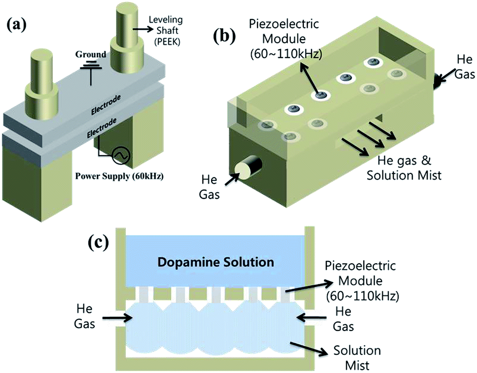 | ||
| Fig. 1 Schematic drawing of the polydopamine-like coating module composed of a plasma module and a gas mixture module. (a) DBD-type atmospheric pressure plasma module, (b) dopamine solution gas mixture module, (c) cross section of the gas mixture module. | ||
Fig. 1(b) shows the piezoelectric module for the supply of dopamine and He to the plasma chamber in Fig. 1(a). As mentioned earlier, the dopamine itself has an extremely low vapor pressure at room temperature and easily dissociated at the temperature of 250 °C, therefore, it is impossible to supply dopamine vapor as the precursor to the deposition chamber for polymerization in Fig. 1(a). Instead, the dopamine is easily dissolved in water like sugar or salt. Therefore, to inject dopamine in the plasma, a dopamine solution was injected to the plasma as a mist using a piezoelectric spray method as shown in Fig. 1(c). For the supply of a solution into the plasma, a mist sprayed by a spray gun has been used by previous researchers.27 However, in this study, to decrease the mist size and to supply the mist more uniformly, a piezoelectric spray (ultrasonic atomization) method has been applied for the supply of the dopamine solution mist into the atmospheric pressure plasma system.28 Differently from an air spray gun.29,30 which uses air pressure for the generation of a mist, the piezoelectric spray method uses a piezoelectric module vibrating 60–110 kHz for generating a mist from a solution and it tend to generate smaller size mist and use smaller material in generating the mist. As shown in Fig. 1(b), to induce the dopamine mist into the atmospheric pressure module, 9 piezoelectric devices (MANORSHI, MNSE2517B-W) were installed in the piezoelectric module and the dopamine solution was fed from the edge of the piezoelectric devices in the module to form a mist in the gas mixing chamber as shown in Fig. 1(c) (see the details of the piezoelectric device in ESI Fig. S1†). Helium (He) was fed from the side of the gas mixing chamber as shown in Fig. 1(b) and (c) to form a gas mixture composed of dopamine solution mist and He as a carrier gas and plasma generation gas.
2.2 Atmospheric pressure plasma coating module
2 gram of dopamine powder (Sigma Aldrich, H8502) was mixed in a beaker with 100 ml of deionized (DI) water and was dispersed by a sonicator for 5 min to form a dopamine solution. Polydopamine-like polymer film coating process steps are as shown in Fig. 2.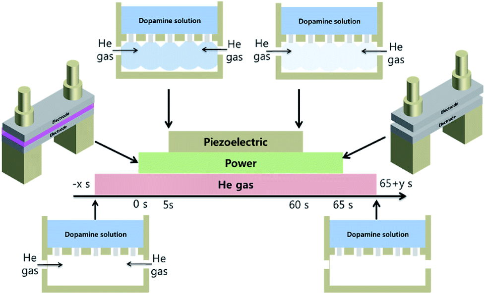 | ||
| Fig. 2 Process sequence for polydopamine-like polymer thin film coating. | ||
As the silicon substrate was loaded in the atmospheric pressure plasma process chamber, 15 SLM of He is flowed in the process chamber through the gas mixing chamber, and the plasma is turned on by operating the DBD source with He only. After ∼5 s later, the piezoelectric module is turned on to induce a gas mixture composed of He and the dopamine solution mist for 60 s into the plasma process chamber for the deposition of the polydopamine-line film on the substrate. After ∼5 s later after the piezoelectric module was turned off, the plasma is turned off and He flow is also turned off after 5 s more to remove all the dopamine mist from the chamber. As the power to the DBD source, different voltages of 1.5, 2.0, 2.5, and 3.0 kV were used to investigate the possibility of polymer deposition with the Stille mechanism.
2.3 Analysis and measurements
Chemical and physical properties of the polymer deposited by the atmospheric pressure plasma using the dopamine solution mist and He were investigated. The surface energy of the deposited polymer films was investigated using a contact angle analyzer (SEO, Phoenix 450). The surface roughness of the polymer deposited on the silicon wafer was measured using an atomic force microscope (AFM, XE150-PSIA). The surface morphologies of the deposited polymer films and metals adsorbed on the polymer surface during the metal absorption test (described in the next section) were observed with a field emission scanning electron microscope (FE-SEM, HITACHI, S-4700). The thickness of the polymer thin film deposited on the silicon wafer was measured using the cross-sectional SEM after the cutting of the polymer deposited silicon wafer in the liquid nitrogen. The binding states and chemical composition of the polymer surface after the metal absorption test shown below were measured using X-ray photoelectron spectroscopy (XPS, Thermo VG SIGMA PROBE). The functional groups of dopamine in the deposited polymer thin film were investigated using Fourier-Transform infrared spectroscopy (FT-IR, Bruker, IFS-66/S).2.4 Metal absorption test
Metal absorption properties of the polydopamine-like polymer film deposited on the silicon substrate were investigated by immersing the substrate in a 0.01 mole chromium chloride solution and a 0.01 mole silver nitrate solution for 6 h. The 0.01 mole chromium chloride solution and 0.01 mole silver nitrate solution were made by mixing 2.66 g of chromium chloride hexahydrate (Avention, c100293) and 1.69 g of silver nitrate (Daejung, 7761-88-8) in 1.0 l of DI water, respectively. The 10 mm × 10 mm substrates coated with the polymer were immersed in 100 ml of the solutions for 6 h and the surface characteristics were measured using SEM and XPS.The metal absorption property of the polydopamine-like film was compared with other commercial metal absorption materials for waste water treatment such as two ion exchange resin bead materials (IR120 and HCR-S by DOW) and one arsenic/metal removal filter bead material (A600 by DOW). Due to the differences in surface area of the materials, the actual surface areas of the materials in contact with the metal containing solution were calculated and the same surface area of 10 mm × 10 mm was used for the accurate test. For the metal absorption test, metal solutions containing 100 ppm of metal such as copper nitrate trihydrate (Junsei, 37510s0401), arsenic standard solution (Kanto chemical, 01805-1b), and chromium chloride hexahydrate (Avention, c100293) were prepared and IR120, HCR-S, and A600 were immersed in the solution together with the substrate coated with the polydopamine-like film for 24 h (for saturation absorption) and the metal residue remaining in the solution was measured using inductively couple plasma-optical emission spectrometry (ICP-OES, Varian) for the calculation of metal removed by the materials (absorption weight per area).
3. Results and discussion
Using the DBD-type atmospheric pressure plasma source and with a piezoelectric spray supplying a dopamine solution mist and He, polymer thin films were deposited on the silicon wafer for 60 s as shown in Fig. 2 and the surfaces of silicon wafer before and after the thin film coating are shown in Fig. 3. As shown in Fig. 3(a) and (b), after the plasma processing for 60 s with 1.5 kV of DBD voltage, a material was deposited on the silicon surface even though somewhat non-uniform coating was observed on the silicon surface possibly due to the scattering of the mist on the silicon surface. Also, for the other DBD voltages of 2.0, 2.5, and 3.0 kV, as shown in Fig. 3(c)–(e), thin films were also coated on the surface, however, as the voltage to the DBD electrode is increased, a thin film morphology with blisters was observed and the blister density was increased. It is believed that the blister is related to damage to the polymer at the high operation DBD voltage. Dopamine contains nitrogen in its molecular structure (C8H11NO2) as an amine functional group and the ratio of N/C related to the amine group in the dopamine and polydopamine is known to be ∼10%.1 Therefore, using XPS, N1s XPS narrow scan data were measured for the polydopamine-like polymer thin films deposited as a function of DBD voltages from 1.5 to 3.0 kV and the results are shown in Fig. 4. As shown, for the As-is silicon wafer, no nitrogen peak was detected but, after the deposition of the polymer thin films, nitrogen peak intensity at the binding energy of about 398–400 eV which is related to the R-NH could be observed.31 As shown in Fig. 4, with the decrease of DBD voltage, the nitrogen peak in the polymer thin film was increased and, when the ratio of N/C was measured, the ratio was also increased from 2.6 to 6.8% as the DBD voltage is decreased from 3.0 to 1.5 kV possibly indicating increased percentage of dopamine monomer deposition without breaking the functional groups by Stille mechanism.14–16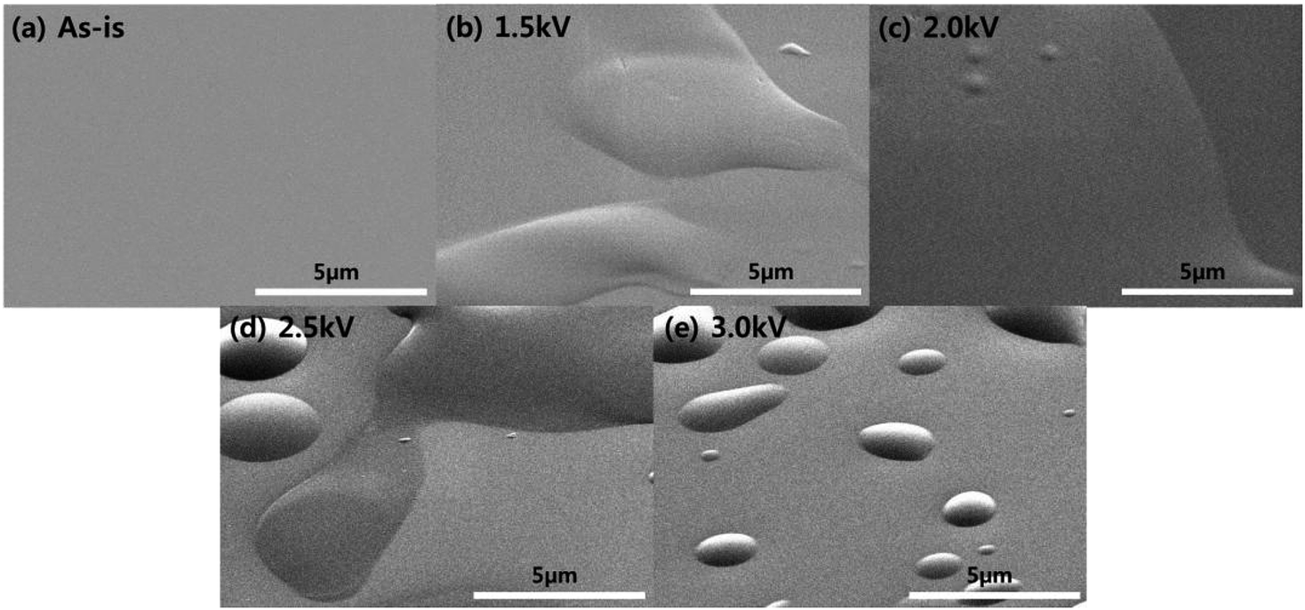 | ||
| Fig. 3 SEM images before and after the polydopamine-like polymer coating for different DBD power voltages. (a) As-is (silicon wafer), (b) 1.5 kV, (c) 2.0 kV, (d) 2.5 kV, and (e) 3.0 kV of DBD voltages. | ||
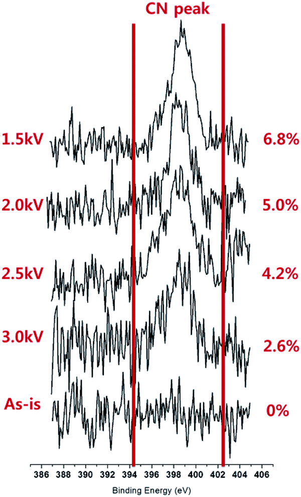 | ||
| Fig. 4 XPS nitrogen (N1s) peak intensity and the ratio of N/C measured on the silicon substrate before and after deposition of polydopamine-like film as a function of DBD voltage for 60 s. | ||
To investigate the possibility of preserving the other functional groups of dopamine in the deposited polymer further, the characteristics of deposited polymer films were investigated using FTIR and the results are shown in Fig. 5 for the polymer film deposited with the DBD voltage from 1.5 to 3.0 kV. As shown in Fig. 5, the absorption peaks related to benzene ring peak (1600–1580 cm−1 and 1510–1500 cm−1, catechol functional group of dopamine) and hydroxyl group peak (3400–3000 cm−1) which are the functional groups of dopamine could be observed on the deposited polymer films.32–35 The decrease of DBD voltage from 3.0 to 1.5 kV increased the absorption peak intensity related to the benzene ring while decreasing the absorption peak intensity related to hydroxyl group. The hydroxyl group in the deposited films can also originate from the dissociated H2O in the dopamine solution mist, therefore, the change of the benzene ring peak intensity not the hydroxyl group peak intensity can indicate the degree of functional group preservation in the deposited polymer film without breaking the functional groups of dopamine. From the results of Fig. 4 and 5, it is found that, by using the lower DBD voltage, more polydopamine-like thin film which has more functional groups of dopamine could be deposited. The adhesive properties of polydopamine deposited on the substrate can be indirectly measured by water contact angle on the surface and the lower the contact angle indicates higher the adhesion to the other materials.38,39
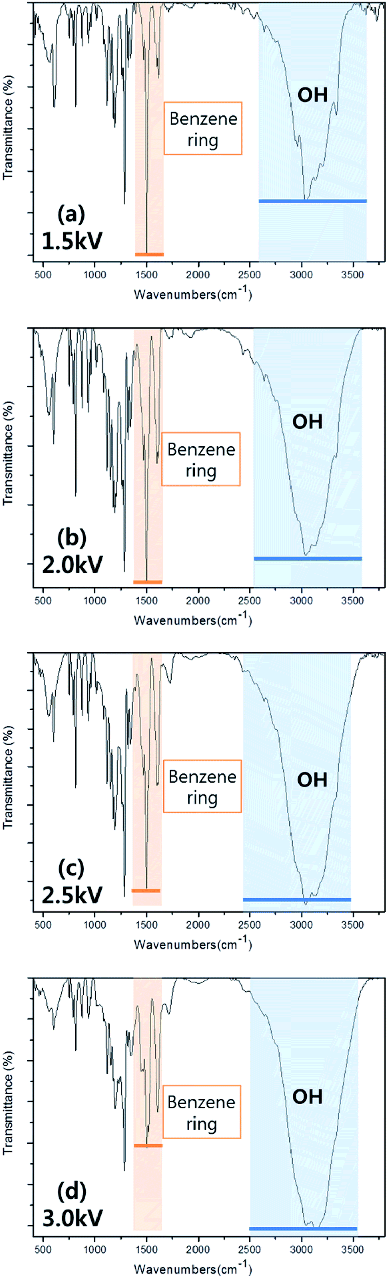 | ||
| Fig. 5 FT-IR absorption peak intensity of polydopamine-like films deposited at different DBD voltages. (a) 1.5 kV, (b) 2.0 kV, (c) 2.5 kV, and (d) 3.0 kV. | ||
Fig. 6 shows the water contact angles measured on the silicon substrates exposed to the plasmas of different DBD voltages for the deposition of polydopamine-like polymer films.
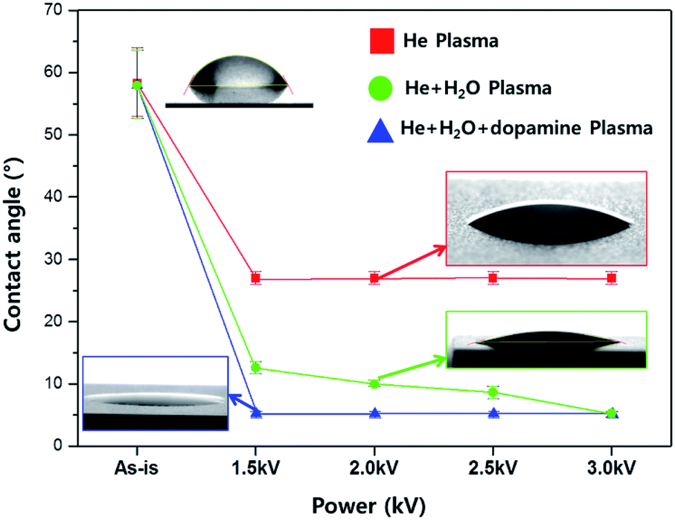 | ||
| Fig. 6 Water contact angles on the silicon substrates measured at different DBD voltages for the deposition of polydopamine-like polymer films. In addition to the gas mixture condition for the deposition of polydopamine-like thin films which is composed of He/dopamine mist (H2O + dopamine), the gas conditions of He only and He/H2O mist without dopamine were also investigated. | ||
As the gas conditions for the plasma exposure, in addition to the gas mixture condition for the deposition of polydopamine-like thin films which is composed of He/dopamine mist (H2O + dopamine), the gas conditions of He only and He/H2O mist without dopamine were investigated. The exposure times was 60 s. As shown in Fig. 6, for the As-is silicon substrate, the water contact angle was 53–64°, and when the silicon substrate was exposed to He plasma (red square), the contact angle was decreased to 26–27° possibly due to the surface cleaning,26 however, no noticeable change with increasing the DBD voltage was observed. When the substrate was exposed to He + H2O (green circle) plasma, the contact angle was continuously decreased with increasing the DBD voltage from 12° (at 1.5 kV) to 5–6° (at 3.0 kV) and the continuous decrease of contact angle with increasing the DBD voltage is believed to be related to the surface modification of silicon surface by the formation of hydroxyl group.23 However, in the case of silicon exposed to the He + H2O + dopamine plasma (blue triangle) which is the gas mixture for the polydopamine-like film deposition, the contact angle was suddenly decreased to the minimum of 5–6° at 1.5 kV and was remained similar to 3.0 kV, and which indicates the lowest contact angle at 1.5 kV with He + H2O + dopamine plasma due to the formation of functional groups of dopamine in the polydopamine-like polymer film deposited on the silicon surface.
To investigate the actual metal absorption characteristics of the polydopamine-like polymer films, the polymer thin films deposited on silicon substrates were immersed in 0.01 M silver nitrate solution and 0.01 chromium chloride solution for 6 h and their metal absorption characteristics were investigated. Fig. 7 and 8 show the SEM images of the polymer film surfaces deposited at different DBD voltages after the exposure in 0.01 M silver nitrate solution and 0.01 chromium chloride solution, respectively, for 6 h. As shown in Fig. 7 and 8, the absorption of metal particles on the polydopamine-like polymer surfaces could be identified and the polymer film deposited at lower DBD voltage exhibited smaller particles shapes and larger area coverage of absorbed metal compared to that deposited at higher DBD voltages. In fact, for the condition of 1.5 kV of Fig. 7 (a) and 8(a), the due to the high coverage of metal on the surface, almost metal thin film was formed in addition to the particles on the polymer surface.
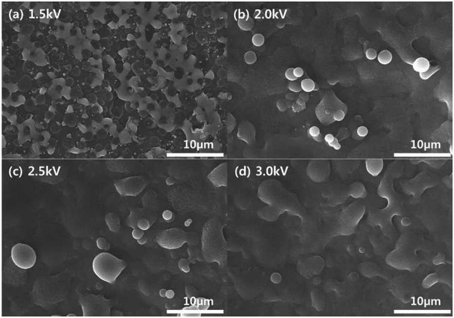 | ||
| Fig. 7 SEM images of polydopamine-like films deposited at different DBD voltages after absorption of silver by exposing to 0.01 M silver nitrate solution for 6 h. (a) 1.5 kV, (b) 2.0 kV, (c) 2.5 kV, and (d) 3.0 kV. | ||
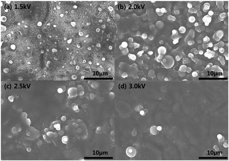 | ||
| Fig. 8 SEM images of polydopamine-like films deposited at different DBD voltages after absorption of silver by exposing to 0.01 M chromium chloride solution for 6 h. (a) 1.5 kV, (b) 2.0 kV, (c) 2.5 kV, and (d) 3.0 kV. | ||
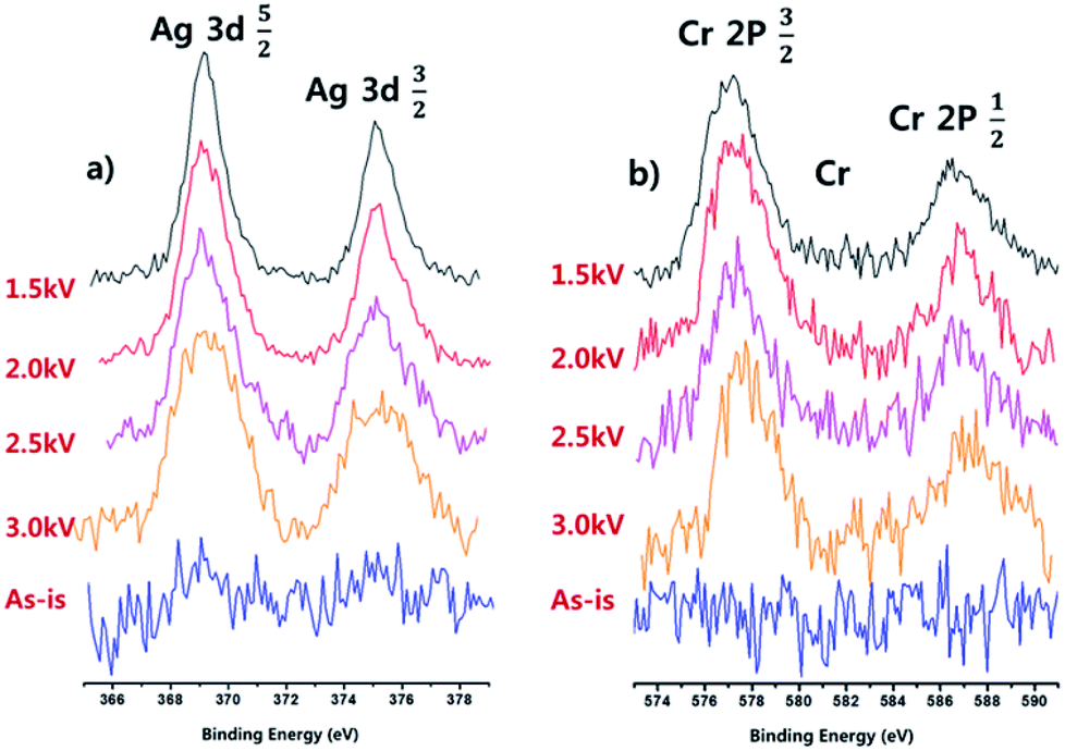
The polymer thin films exposed to the 0.01 M silver nitrate solution and 0.01 chromium chloride solution for 6 h in Fig. 7 and 8 were also investigated using XPS to measure the degree of metal absorption more quantitatively and the results are in Fig. 9(a) for Ag and (b) for Cr. As shown in Fig. 9 (a) and (b), the Ag peak intensities at 3d5/2 (368 eV) and 3d3/2 (374 eV) and Cr peak intensities at 2P3/2 (577 eV) and 2P1/2 (587 eV).36,37 could be observed while no such peak intensities were observed for As-is silicon substrate, and the peak intensities of Ag and Cr were increased with the decrease of DBD voltage due to the increased metal absorption on the polymer surface during the immersion in the metal solution. The percentages of Ag and Cr on the polymer surfaces after the immersion in the silver nitrate solution and chromium chloride solution for 6 h were measured by XPS and the results are shown in Table 1. As shown in Table 1, the decrease of DBD voltage from 3.0 kV to 1.5 kV increased the percentages of Ag from 2.66% to 7.63% and that of Cr from 3.24% to 11.68%.
 | ||
| Fig. 9 XPS narrow scan peak intensities of (a) Ag and (b) Cr on the polydopamine-like polymer deposited at different DBD voltages after exposure to 0.01 M silver nitrate solution and 0.01 chromium chloride solution for 6 h. | ||
| Power | Ag% | Cr% |
|---|---|---|
| 1.5 kV | 7.63 | 11.68 |
| 2.0 kV | 4.37 | 5.5 |
| 2.5 kV | 3.29 | 4.8 |
| 3.0 kV | 2.66 | 3.24 |
As can be seen in Fig. 4 and 5, more functional groups of dopamine can remain unbroken by using a plasma polymerization with a lower electron energy and, it is found that the characteristic of polydopamine as the metal absorber remain more on the deposited polydopamine-like polymer film when more functional groups of dopamine remain in the polymer film by measuring the contact angle, metal absorption percentages, etc. as shown in Fig. 6–9.
To study the characteristics of the polydopamine-like polymer thin film as metal absorbers further, the polydopamine-like polymer thin film deposited at DBD voltage of 1.5 kV for 60 s was immersed in various metal containing solutions such as copper nitrate trihydrate, arsenic standard solution, and chromium chloride hexahydrate and its metal absorption characteristics were compared with other commercial metal absorption materials such as two ion exchange resin bead materials (IR120 and HCR-S) and one arsenic/metal removal filter bead material (A600) in addition to As-is silicon substrate as the reference. For the accurate comparison of metal absorption, the materials with the same surface area of 100 mm2 were immersed for 24 h in the three different metal containing solutions and the remaining metal contents in the metal containing solutions were measured by ICP-OES for the calculation of absorption weight/unit area, and the results are shown in Fig. 10. As shown in Fig. 10, the metal absorption characteristics of As-is silicon substrate were generally low for all metals while IR 120 showed the highest Cr absorption characteristics and HCR-S showed the next highest Cr absorption characteristics because they are Cr-targeted metal absorbers. In the case of the polydopamine-like polymer film, it generally exhibited superior metal absorption characteristics for all metals by showing similar Cr absorption as HCR-S, 113% higher for As absorption compared to A600 (As-targeted material), and 216% higher than IR 120 for Cu absorption.
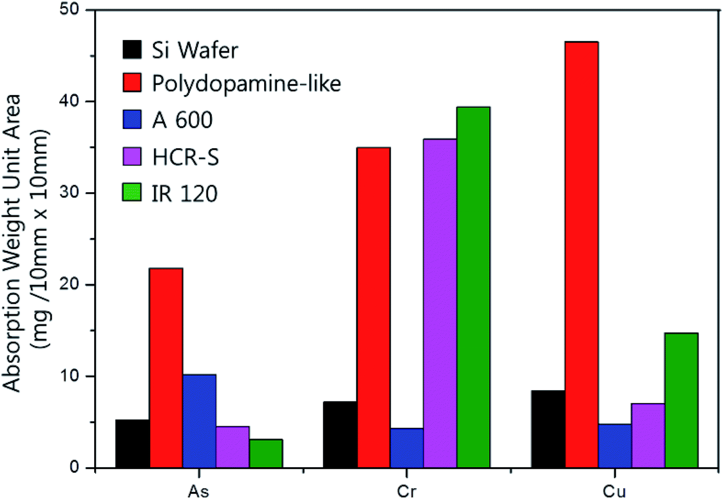 | ||
| Fig. 10 Metal absorption weight/unit area for different metal absorption materials. As the metal absorption materials, commercial materials such as ion exchange resin bead materials (IR120 and HCR-S) and one arsenic/metal removal filter bead material (AS600) in addition to the silicon wafer deposited with the polydopamine-like thin film at 1.5 kV for 60 s were included. The materials with the same surface area of 100 mm2 were immersed for 24 h in the three different metal containing solutions of copper nitrate trihydrate, arsenic standard solution, and chromium chloride hexahydrate. After the immersion of materials for 24 h, the remaining metal content was measured by ICP-OES for the calculation of absorption weight/unit area. | ||
Therefore, by depositing polydopamine-like polymer film without breaking the functional groups of dopamine by using the low energy atmospheric pressure plasma and with a dopamine solution mist, the superior metal absorption characteristics similar to polydopamine itself deposited by the wet method could be obtained.
Finally, for the DBD voltage of 1.5 kV, the thickness and surface roughness of polydopamine-like thin film were measured with increasing deposition time to 60 s and the results are shown in Fig. 11 and 12, respectively. As shown in Fig. 11, the film thickness increased almost linearly with increasing deposition time but, there appears to be an incubation time for deposition of about 15 s. The thickness deviation was also increased with increasing thickness (details are in Fig. S2†). In the case of surface roughness, as shown in Fig. 8, the surface roughness was increased with the increasing polydopamine thickness. For the 15 s deposition, and the surface roughness was ∼2 nm (the thickness of polydopamine-like film was ∼30 nm) and, for the 60 s deposition, the surface roughness was increased to 84 nm (the thickness of polydopamine-like film was ∼536 nm), therefore, the roughness was increased with the increased polydopamine-like film thickness, and the surface roughness was ≤15% of the thickness.
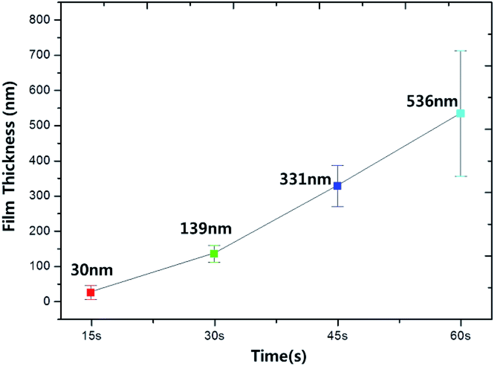 | ||
| Fig. 11 Polydopamine-like thin film thickness measured as a function of deposition time at the DBD voltage of 1.5 kV. | ||
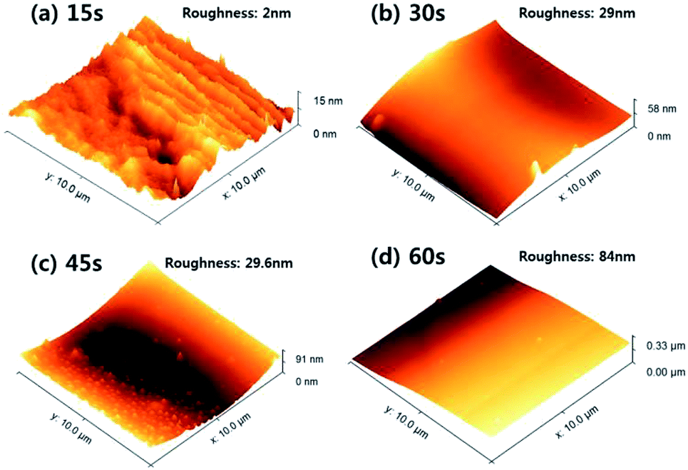 | ||
| Fig. 12 Surface roughness of the polydopamine-like thin film deposited on silicon wafers measured as a function of deposition time. (a) 15 s, (b) 30 s, (c) 45 s, and (d) 60 s at the DBD voltage of 1.5 kV. | ||
4. Conclusions
Polydopamine is generally coated on the surface of materials by a wet coating method, and the wet coating method takes more than a day for the self-polymerization of dopamine. In this study, by using atmospheric pressure plasmas with a low electron energy and a dopamine solution mist formed by piezoelectric module, polymer films showing the physical and chemical characteristics of polydopamine could be deposited in 60 s on the material surface. By using the atmospheric pressure plasma with the lower DBD voltage of 1.5 kV, the partial dissociation of dopamine molecule for polymerization without breaking the catechol/amine functional groups of dopamine suggested by Stille mechanism could be achieved while the use of the higher DBD voltage to 3.0 kV tends to break more functional groups of dopamine into atoms as suggested by Yasuda's atomic polymerization mechanism which leads to the decreased physical and chemical characteristics of polydopamine. It is believed that this atmospheric pressure plasma polymerization method of dopamine can be applied to various areas which require surface modifications instantly by forming a polydopamine film similar to the wet methods and by enabling in-line and roll-to-roll processes in the atmospheric pressure without using vacuum system. Also, it is believed that this process can be applied to the plasma polymerization of various other monomers without breaking functional groups of the monomers.Conflicts of interest
There are no conflicts to declare.References
- H. S. Lee, S. M. Dellatore, W. M. Miller and P. B. Messersmith, Science, 2007, 318, 426–430 CrossRef CAS PubMed.
- Y. S. Choi, D. G. Kang, Y. J. Yang, C. S. Kim and H. J. Cha, Biofouling, 2011, 27, 729–737 CrossRef CAS PubMed.
- S. H. Ku, J. K. Ryu, S. K. Hong, H. S. Lee and C. B. Park, Biomaterials, 2010, 31, 2535–3541 CrossRef CAS PubMed.
- T. Akter and W. S. Kim, ACS Appl. Mater. Interfaces, 2012, 4, 1855–1859 CrossRef CAS PubMed.
- E. W. Danner, Y. Kan, M. U. Hammer, J. N. Israelachvili and J. H. Waite, Biochemistry, 2012, 51, 6511–6518 CrossRef CAS PubMed.
- L. Tan, L. Pan, C. Cao, B. Wang and L. Li, J. Power Sources, 2014, 253, 193–200 CrossRef CAS.
- H. Li, L. Shen, K. Yin, J. Ji, J. Wang, X. Wang and X. Zhang, J. Mater. Chem. A, 2013, 1, 7270–7276 RSC.
- Y. X. Dong, J. T. Cao, Y. M. Liu and S. H. Ma, Biosens. Bioelectron., 2017, 91, 246–252 CrossRef CAS PubMed.
- C. Zhang, Y. Ou, W. X. Lei, L. S. Wan, J. Ji and Z. K. Xu, Angew. Chem., 2016, 128, 3106–3109 CrossRef.
- X. Du, L. Li, J. Li, C. Yang, N. Frenkel, A. Welle, S. Heissler, A. Nefedov, M. Grunze and P. A. Levkin, Adv. Mater., 2014, 26, 8029–8033 CrossRef CAS PubMed.
- Z. Wang, C. Xu, Y. Lu, G. Wei, G. Ye, T. Sun and J. Chen, Polym. Chem., 2017, 8, 4388–4392 RSC.
- V. K. Thakur, M. F. Lin, E. J. Tan and P. S. Lee, J. Mater. Chem., 2012, 22, 5959 RSC.
- S. I. Kim, D. Y. Lee and H. S. Lee, J. Korean Vac. Soc., 2014, 2, 121 Search PubMed.
- J. K. Stille, R. L. Sung and J. V. Kooi, J. Org. Chem., 1965, 30, 3116 CrossRef CAS.
- J. Friedrich, Plasma Processes Polym., 2011, 8, 783–802 CrossRef CAS.
- D. Merche, N. Vandencasteele and F. Reniers, Thin Solid Films, 2012, 520, 4219–4236 CrossRef CAS.
- H. Yasuda and C. R. Wang, J. Polym. Sci., Part A-1: Polym. Chem., 1985, 23, 87–106 CAS.
- D. R. Dreyer, D. J. Miller, B. D. Freeman, D. R. Paul and C. W. Bielawski, Langmuir, 2012, 28, 6428–6435 CrossRef CAS PubMed.
- S. M. Kang, N. S. Hwang, J. H. Yeom, S. Y. Park, P. B. Messersmith, I. S. Choi, R. Langer, D. G. Anderson and H. S. Lee, Adv. Funct. Mater., 2012, 22, 2949–2955 CrossRef CAS PubMed.
- C. H. Lee, J. S. Shin, J. S. Lee, E. K. Byun, J. H. Ryu, S. H. Um, D. I. Kim, H. S. Lee and S. W. Cho, Biomacromolecules, 2013, 14, 2004–2013 CrossRef CAS PubMed.
- S. Bornholdt, M. Wolter and H. Kersten, Eur. Phys. J. D, 2010, 60, 653–660 CrossRef CAS.
- X. P. Zou, E. T. Kang, K. G. Neoh and W. Huang, J. Adhes. Sci. Technol., 2012, 15, 1655–1672 CrossRef.
- Y. Lin, C. Chen, C. Wang, F. Pu, J. Ren and X. Qu, Chem. Commun., 2011, 47, 1181–1183 RSC.
- H. Zhang, L. Bré, T. Zhao, B. Newland, M. D. Costa and W. Wang, J. Mater. Chem. B, 2014, 2, 4067–4071 RSC.
- M. K. Mun, J. W. Park, J. H. Ahn, K. K. Kim and G. Y. Yeom, J. Nanosci. Nanotechnol., 2015, 15, 8176–8182 CrossRef CAS PubMed.
- M. K. Mun, J. W. Park and G. Y. Yeom, Plasma Processes Polym., 2016, 13, 722–729 CrossRef CAS.
- C. Bingyan, Z. Changping, F. Juntao, H. Xiang, Y. Cheng, W. Yuan, J. Yongfeng, C. Lonwei, G. Yuan and H. Qingbang, Plasma Sci. Technol., 2016, 18, 41–50 CrossRef.
- S. Slegers, M. Linzas, J. Drijkoningen, J. D'Haen, N. K. Reddy and W. Deferme, Coatings, 2017, 7, 208 CrossRef.
- H. Yuasa, T. Nakano and Y. Kanaya, Int. J. Pharm., 1999, 178, 1–10 CrossRef CAS PubMed.
- M. A. Mugele and H. D. Evans, Ind. Eng. Chem., 1951, 43, 1317–1324 CrossRef.
- Y. Hayashi, G. Yu, M. M. Rahman, K. M. Krishna, T. Soga, T. Jimbo and M. Umeno, J. Appl. Phys., 2001, 89, 7924 CrossRef CAS.
- T. López, P. Quintana, J. M. Martínez and D. Esquivel, J. Non-Cryst. Solids, 2017, 353, 987–989 CrossRef.
- J. Tang, X. Jing, B. Wang and F. Wang, Synth. Met., 1988, 24, 231–238 CrossRef CAS.
- A. Kolodziejczak-Radzmska, E. Markiewicz and T. Jesionowski, J. Nanomater., 2012, 2012, 9 Search PubMed.
- N. Krshnamurthy, I. L. Kamel and Y. Wei, J. Polym. Sci., Part A-1: Polym. Chem., 1989, 27, 1211–1224 CrossRef.
- J. H. Kang, S. Tada, T. Kitajima, T. I. Son, T. Aigaki and Y. Ito, BioMed Res. Int., 2013, 2013, 6 Search PubMed.
- Y. J. Chuah, Y. T. Koh, K. Lim, N. Menon, Y. Wu and Y. Kang, Sci. Rep., 2015, 5, 18162 CrossRef CAS PubMed.
- S. Zanna, C. Saulou, M. Mercier-Bonin, B. Despas, P. Raynaud, A. Seyeux and P. Marcus, Appl. Surf. Sci., 2010, 256, 6499–6505 CrossRef CAS.
- J. A. Slotwinski, E. J. Garboczi, P. E. Stutzman, C. F. Ferraris, S. S. Watson and M. A. Peltz, J. Res. Natl. Inst. Stand. Technol., 2014, 119, 460–493 CrossRef CAS PubMed.
Footnote |
| † Electronic supplementary information (ESI) available. See DOI: 10.1039/c8ra10391g |
| This journal is © The Royal Society of Chemistry 2019 |