
 Open Access Article
 This Open Access Article is licensed under a Creative Commons Attribution-Non Commercial 3.0 Unported Licence
High-performance inverted organic light-emitting diodes with extremely low efficiency roll-off using solution-processed ZnS quantum dots as the electron injection layer†
Guanjie Shiab,
Xiaozheng Zhanga,
Minqiang Wana,
Shuanglong Wangb,
Hong Lianb,
Run Xua and
Wenqing Zhu *ab
*ab
aSchool of Materials Science and Engineering, Shanghai University, Shanghai 200072, People's Republic of China. E-mail: wqzhu@shu.edu.cn
bSchool of Mechatronic Engineering and Automation, Key Laboratory of Advanced Display and System Applications, Ministry of Education, Shanghai University, Shanghai, 200072, China
First published on 19th February 2019
Abstract
The electron-injecting layer (EIL) is one of the key factors in inverted organic light-emitting diodes (OLEDs) to realize high electroluminescence efficiency. Here, we proposed a novel cathode-modified EIL based on ZnS quantum dots (QDs) in inverted OLEDs, and demonstrated that the device performance was dramatically improved compared to traditional ZnO EIL. The EIL of ZnS QDs may greatly promote the electron injection ability and consequently increase the charge carrier recombination efficiency for the device. We also investigated the effects of different pH values (ZnS-A, pH = 10; ZnS-B, pH = 12) on the properties of ZnS QDs. The best inverted phosphorescent OLED device employing mCP:Ir(ppy)3 as the emission layer showed a low turn-on voltage of 2.9 V and maximum current efficiency of 61.5 cd A−1. Also, the ZnS-A based device exhibits very-low efficiency roll-off of 0.9% and 4.3% at 1000 cd m−2 and 5000 cd m−2, respectively. Our results indicate that use of ZnS QDs is a promising strategy to increase the performance in inverted OLEDs.
Introduction
New-generation organic light-emitting diodes (OLEDs) are promising candidates for solid state lighting and display devices with the ever-growing demand because of their distinguishing advantages such as low power consumption, flexibility, wide viewing angle, and vivid colors.1–4 An important factor for the commercialization of OLED displays is related to their intrinsic driving method. Although the active matrix OLEDs (AMOLEDs) have been commercialized in flat panels and mobile phones, there still exist some technical issues for their applications. Most mobile AMOLED panels use low temperature poly-silicon thin film transistors (LTPS TFTs) instead of amorphous silicon (a-Si) TFT because of their high mobility and good stability.5–8 However, uniformity and high cost of LTPS are persistent challenges for large-area AMOLED devices. Oxide TFTs can be a solution to this problem by offering high mobility and transparency. Since the majority of oxide TFTs have n-type characteristics, inverted OLED structure is more suitable for the mass production and inverted OLED with bottom cathode can be directly connected to the drain electrode of n-type oxide TFT.9,10 Moreover, inverted OLED structures have several advantages over normal architecture OLEDs.11,12 For example, the device lifetime can be largely enhanced because water- and oxygen-sensitive electron injection materials can be kept beneath the organic and metal layers. Nevertheless, there are still some problems for developing high performance inverted OLEDs such as low efficiency and high operating voltage.13–15One major issue in inverted OLEDs is electron injection from the conducting bottom cathode to the organic semiconductors because of the high energy barrier between the bottom cathode and organic layers. Thus, electron injection layers (EILs) play an important role in the inverted OLEDs.16,17 To solve these issues, various kinds of electron injection materials have been developed by modify the indium tin oxide (ITO) electrode to enhance the electron injection efficiency and increase electron–hole recombination efficiency especially for and solution-processed metal oxide electron injection layers such as ZnO, TiO2 and ZrO2 due to their air stability, nontoxicity, transparency and high electron mobilities.18–20 However, the efficiencies of these inverted OLEDs based on these n-type metal oxides were less than satisfactory because there is still a large electron injection barrier from their conduction band to the lowest unoccupied molecular orbital (LUMO) of the emitters.21,22 For example, the work function of ZnO is about ∼4.4 eV, and the work function of as-deposited TiO2 is about ∼4.4–4.5 eV which are much deeper than the LUMO level of the traditional organic emission materials (2.8–3.0 eV).23,24 This large potential barrier can significantly reduce the electron injection efficiency for devices, resulting in the unbalanced charge-carrier recombination and thus lower the device performance. One approach is to build an interface dipole moment oriented away from the cathode contact, pulling up the vacuum level of the cathode and lowering the electron injection barrier.25,26 Wei et al. demonstrated the successful application of evaporated ZnS film as electron injection materials in fluorescent and phosphorescent OLEDs to enhance electron injection and mitigate the operation voltage in inverted OLEDs.27 However, the high-temperature deposited process limited its practical large-scale and low-coat applications.
More recently, the metal sulfide quantum dots (QDs), on the other hand, are a large family of inorganic materials with core–shell structures have attracted much attention which may play an important role in enhancing electron injection dynamics and optoelectronic device performances, has not been examined.28,29 They possess exceptional properties, such as excellent solubility in water-alcoholic solvent, high transparency in the visible region, adequate electron mobility and facile solution process-ability, which contribute to their outstanding versatility and applications in research areas including catalysis, energy conversion, and molecular electronics.30–32 From this viewpoint, ZnS QDs can be a very promising candidate for the efficient electron injecting material to replace the traditional ZnO injection layer in large-scale and vacuum-free fabricated OLEDs.
Here, we report an inverted OLEDs using the solution-processed ZnS QDs as EIL because of their high performances in inverted devices. We verified the suitability of solution-processed ZnS QDs for use in inverted OLEDs by using various types of analytical methods. The various pH effect plays an essential role in changing properties of ZnS QDs (ZnS-A, pH = 10; ZnS-B, pH = 12). The turn-on voltage of device based on ZnS QDs EIL based was obviously decreased, indicating clearly a reduced electron injection barrier was obtained in the device, and thus the enhanced device performance was attributed to the more balanced charge injection from electrodes in the device. Notably, our device exhibits a surprisingly very low roll-off character and the best inverted OLED employing ZnS-A as the EIL exhibited a highest current efficiency of 61.5 cd A−1 with an extremely small current efficiency roll-off of 0.9% and 4.3% at 1000 cd m−2 and 5000 cd m−2, respectively, achieving a current efficiency enhancement of 23.7% than those with ZnO EIL.
Experimental
General information
All chemicals and regents in this work were used as received from commercial sources without purification unless otherwise stated. The other organic functional molecules were obtained from e-Ray Optoelectronics Corp. (Taipei, Taiwan). Molybdenum(VI) oxide (99.99%). The reference device used ZnO ethanol solution and the chemicals needed to synthesize quantum dot solutions were purchased from Sigma-Aldrich. Indium tin oxide (ITO, 15 Ω per sheet, 150 nm)-coated glass substrates were ordered from CSG Holding Co. Ltd (China).Synthesis of ZnS QDs
100 mL of a 0.1 mol L−1 Na2S aqueous solution was prepared. The amount of Na2S·9H2O required is calculated as 2.4018 g. Take out the 2.4018 g Na2S·9H2O medicine with a precision electronic scale, put it into a 100 mL volumetric flask, add distilled water to the 100 mL scale, and mix and store well. Secondly, a 0.1 mol L−1 Zn(CH3COO)2 solution of 0.02 mol L−1 RSH aqueous solution was prepared, and the preparation process was the same as that of the above Na2S aqueous solution. Finally, add 25 mL of the above-prepared 0.1 mol L−1 Zn(CH3COO)2 solution to a three-necked round bottom flask, and continue to add 50 mL of 0.02 mol L−1 ethanethiol acid, and then adjust the pH of the solution by adding 0.5 mol L−1 NaOH solution to 10 and 12 (because of the difference in pH, in order to distinguish pH = 10, it is called ZnS-A, pH = 12 is called ZnS-B). Once the synthesis solution is ready, the three-necked round bottom flask was sealed, and the airtightness of the test device was intact. The oxygen in the device was driven out by nitrogen for 15 minutes. After that, the device was ultrasonicated for 10 minutes, and 7.5 mL of the prepared Na2S aqueous solution was quickly added. Ultrasonic treatment for 30 min. Finally, the mixture was stirred at a water temperature of 80 °C for 90 min to harvest the QDs.Device fabrication
Devices were fabricated in the structure of ITO/ZnS QDs or ZnO/Bphen:Cs2CO3 (20 nm)/Bphen (10 nm)/mCP:Ir(ppy)3 (20 nm)/TCTA (10 nm)/NPB (30 nm)/MoOx (5 nm)/Al (100 nm) under a base pressure lower than 1.0 × 10⁻⁵ mbar unless the solution-processed EIL, where ITO is the anode, 4,7-diphenyl-1,10-phenanthroline (Bphen) doped with Cs2CO3 is the electron injection and transporting layer; 1,3-bis(N-carbazolyl)benzene (mCP) is the host for green phosphorescent dopant; tris(2-phenyl-3-methyl-pyridine)iridium (Ir(ppy)3) is the green dopant, 4,4′,4′′-tris(carbazol-9-yl)triphenylamine (TCTA) and N,N′-bis(naphthalen-1-yl)-N,N′-bis(phenyl)-benzidine (NPB) are the hole transporting layer, MoOx and Al are hole injection layer and anode, respectively. Electron-only devices using the following structure: ITO/EIL/Bphen (120 nm)/Liq (1 nm)/Al (100 nm).Prepared ITO coated glass substrates were cleaned using detergent, de-ionized water, acetone, and isopropanol. Immediately prior to loading into a custom-made high vacuum thermal evaporation chamber, the substrates were treated with a UV-ozone environment for 20 min. After that, the prepared ZnS QDs solutions were spin-coated onto the ITO at 3000 rpm for 60 s, and then annealed at 130 °C for 15 min in ambient atmosphere. Then, organic layers and a metal cathode layer were successfully evaporated by using shadow masks. The entire organic layers, MoOx and the Al cathode were deposited without exposure to the atmosphere, by which OLEDs with an active areas of 4 mm2 were obtained. The deposition rates for the organic materials, MoOx and Al were typically 1.0, 0.3 and 5.0 Å s−1, respectively.
Characterization
The transmittance and photoluminescence (PL) spectra were measured by using an UV-vis spectrophotometer (HITACHI U-3900H) and an FLSP 920 spectrometer series with an excitation wavelength of 300 nm, respectively. Droplet contact angle (CA) measurements were performed using the Kino optical CA and interface tensionmeter in ambient atmosphere. The surface morphological images of the ITO/EIL films were analyzed by using atomic force microscopy (AFM) (Nanonavi SPA-400SPM). The EL characteristics were measured using a Keithley 2400 source meter and a PR650 Spectra Colorimeter under ambient condition at room temperature. The luminance and spectra of each device were measured in the direction perpendicular to the substrate.Results and discussion
According to the different pH values in solution, ZnS QDs divided into ZnS-A (pH = 10) and ZnS-B (pH = 12). The transmittance spectra of the ZnO, ZnS-A and ZnS-B films in the wavelength range 220–800 nm are shown in Fig. 1. The transmittances are over 90% in the visible region. At the green emission spectral range, the bare glass with ZnS-A or ZnS-B yielded a higher transmittance of 92.6% at 520 nm compared to ZnO EIL which is beneficial for improving the light extraction in inverted OLEDs. It also indicates that the different pH values have little effect on the transmittance of ZnS QDs. And the corresponding photoluminescent spectra of ZnO, ZnS-A or ZnS-B film are shown in Fig. S1 (ESI†). | ||
| Fig. 1 Transmittance spectra of various EIL thin films spin-coated on glass, where the EIL indicates ZnO, ZnS-A, or ZnS-B. Inset shows magnified transmittance band edge between 500 and 550 nm. | ||
Considering that the surface wettability of a cathode interlayer in an inverted OLED can determine its interface contact with the adjacent layer for the solution coating process, we measured the CA of water droplets on ZnO, ZnS-A and ZnS-B films. It can be seen in Fig. 2, the contact angles of water on ZnO, ZnS-A and ZnS-B films were 36.8°, 7.8° and 20.6°, respectively. We notice that the contact angles of ZnS QDs, especially for ZnS-A is much smaller than that of ZnO, indicating that doped ZnS QDs spin-coated films are slightly more hydrophilic which is beneficial for the contact with the other layers more efficiently consequently leading to a better adhesion and filming property between cathode and organic functional layers.33
 | ||
| Fig. 2 Photographs of contact angles of the surface for (a) ZnO, (b) ZnS-A and (c) ZnS-B films coated on glass substrate. | ||
AFM measurements were carried out to thoroughly investigate the surface morphology of the various EILs. The height images and the three dimensional surface plot of the ZnO, ZnS-A and ZnS-B films are illustrated on Fig. 2. Obviously, both the ZnS-A and ZnS-B films demonstrate an excellent modification effect on the ITO surface and display relative glossy surface, and the root-mean-square roughness (RMS) of ZnS-A and ZnS-B films is 0.28 and 1.07 nm, respectively, referring that ZnS QDs molecules are prone to fill in the concave sites of ITO surface. And on the other hand, the reference of ZnO film have a highest RMS of 8.92 nm among these three films. From the results, we can clearly see that films coated with ZnS QDs almost remain the identical homogeneous morphologies without apparent surface reconstruction, especially for type of ZnS-A, suggesting that the natural interfacial material possesses uniform film forming performance which is also favourable for an effective injection of charge-carriers (Fig. 3).34
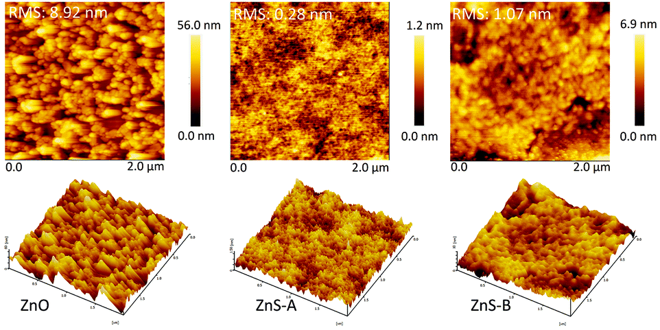 | ||
| Fig. 3 Tapping-mode AFM height images of ZnO, ZnS-A and ZnS-B thin films on ITO glass. All the films were spin-coated onto substrates and annealed at 150 °C for 15 min. The scan area of all images is 2 μm × 2 μm. | ||
Furthermore, to investigate the electrical properties of the three different EILs for use in the inverted device, we fabricated electron-only devices (EODs) with device structures of ITO/EIL/Bphen (120 nm)/Liq (1 nm)/Al (100 nm) with three kinds of cathode injection layers simultaneously and tested the character electron current injected from ITO and the performances of ZnO, ZnS-A or ZnS-B as EILs were compared. We also fabricated reference EODs using the following device structure: ITO/ZnS/Bphen (100 nm)/Liq (1 nm)/Al (120 nm) (Device 1); ITO/Bphen:Cs2CO3 (100 nm)/Liq (1 nm)/Al (120 nm) (Device 2); ITO/Bphen:Cs2CO3 (20 nm)/Bphen (100 nm)/Liq (1 nm)/Al (120 nm) (Device 3) and the relative results are shown in Fig. S2.† The Fig. 4 shows the J–V characteristics of the EODs with different EILs. The device with ZnS QDs EILs showed much higher current than the devices with ZnO EIL indicating the efficient electron injection from both the ZnS-A and ZnS-B. This can be easily understood from the ZnS QDs, which can increase the mobility of carriers and lead to a smaller injection barrier at the contacts associated with efficient injection.
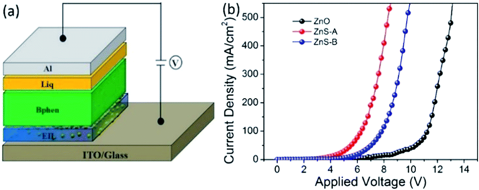 | ||
| Fig. 4 (a) Device configuration of inverted EODs; (b) current density–voltage (J–V) characteristics of electron-only devices of ITO/EILs/Bphen (120 nm)/Liq (1 nm)/Al (100 nm). The EIL indicates ZnO, ZnS-A or ZnS-B. | ||
To evaluate the solution-processed ZnS QDs films as the EIL, the inverted OLEDs were fabricated using the following structure: ITO/EIL/Bphen:CsCO3 (20 nm)/Bphen (10 nm)/mCP:Ir(ppy)3 (20 nm)/TCTA (10 nm)/NPB (30 nm)/MoOx (5 nm)/Al (100 nm), in which the EIL is comprised of ZnO (Device B), ZnS-A (Device C) and ZnS-B (Device D), the device without EIL of ZnO or ZnS was also fabricated as the reference device (Device A), as shown in Fig. 5a. All of the materials structures are displayed in Fig. S3† and the corresponding energy level diagram of inverted OLED devices is shown in Fig. S4.† The details of the device fabrication are given in the Methods. The device structures and the electroluminescent properties are shown in Fig. 5b and summarized in Table 1.
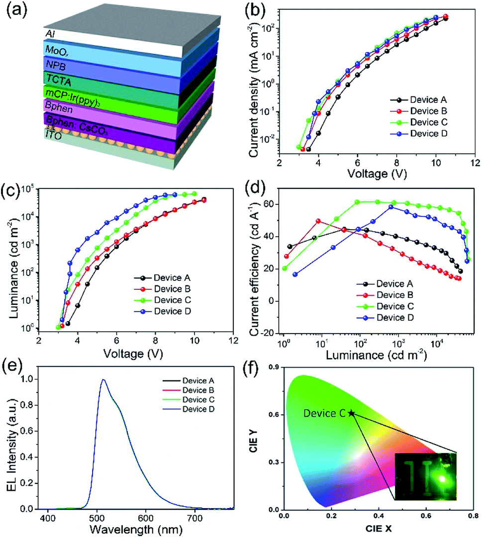 | ||
| Fig. 5 (a) Device configuration of inverted OLEDs. (b) Current density vs. voltage (J–V), (c) luminance vs. voltage (L–V) (d) current efficiency vs. luminance (CE–L) characteristics and (e) electroluminescent spectra at 6 V of inverted bottom emission OLEDs as a function of the electron injection material. (f) The corresponding CIE coordinate of ZnS-A based inverted OLED device (Device C) (the inset of (f) shows photograph of the lighting images of the green emission OLED). | ||
| Devicea | EIL | Vonb [V] | CEc [cd A−1] | PEMaxd [lm W−1] |
|---|---|---|---|---|
| Max/1000/5000 | ||||
| a Device configuration: ITO/EIL/Bphen:Cs2CO3 (20 nm)/Bphen (10 nm)/mCP:Ir(ppy)3 (20 nm)/TCTA (10 nm)/NPB (30 nm)/MoOx (5 nm)/Al (100 nm).b The turn-on voltage at a brightness of 1 cd m−2.c CE at the maximum value/at 1000 cd m−2/at 5000 cd m−2.d PE at the maximum value. | ||||
| A | — | 3.4 | 44.6/39.8/35.1 | 31.1 |
| B | ZnO | 3.2 | 49.7/30.7/22.3 | 44.6 |
| C | ZnS-A | 2.9 | 61.5/60.9/58.8 | 48.2 |
| D | ZnS-B | 3.0 | 58.5/57.3/52.5 | 45.9 |
The use of ZnS QDs EILs dramatically improved the performances of the devices. Fig. 5a shows the J–V characteristics of the devices with different EILs. In the J–V characteristics, the current density begins to increase in the device with ZnS-A or ZnS-B. It clearly demonstrates that the ZnS QDs improves electron injection from EIL to EML due to the lower electron injection barriers. In addition, the device with ZnS QDs showed a higher luminance at same current density and lower turn-on voltage compared with other devices, as shown in Fig. 5b. For instance, the device with ZnO (Device B) showed a turn-on voltage of 3.2 V while other devices (Devices C and D) exhibited lower turn on voltage of 2.9 V and 3.0 V for ZnS-A and ZnS-B, respectively (Fig. 5c). The reference device without EIL (Device A) showed the highest turn-on voltage of 3.4 V due to the large electron injection barrier. The differences are in line with the trend of current density and luminance, which indicates that the injection barriers between ITO cathode and the emitters are crucial factors for the low driving voltage of the best performing device.35
It is noteworthy that the maximum current efficiency of the device with ZnS QDs is much higher than the devices with ZnO. The Device C with ZnS-A as the EIL exhibited extraordinary efficiencies of 61.5 cd A−1 and 48.2 lm W−1 (Fig. 5d). A photograph of Device C is displayed in Fig. 5f. The ZnS-B based Device D also showed excellent efficiency of 58.5 cd A−1 which is more superior to that of Device B which have a current efficiency (CE) of 49.7 cd A−1. Furthermore, both Devices C and D revealed very low efficiency roll-offs. For example, Device C showed a maximum CE of 61.5 cd A−1, and an efficiency of 60.9 cd A−1 at 1000 cd m−2, and 58.8 cd A−1 at 5000 cd m−2, corresponding to a 0.9% and 4.3% decrease in CE, respectively.
The possible reasons for the low efficiency roll-off may attributed to the excellent charge balance of electrons and holes in the device, resulting in improvement of the luminance and efficiency. It is well known that the charge balance of an OLED device, particularly the emitting layer, is also important for reductions in the efficiency roll-off.36 The CEs of four devices at brightness of 1000 cd m−2 and 5000 cd m−2 are summarized in Table 1. The EL spectra of four devices show green emission with peaks at 512 nm, without any emission shift regardless of the different electron injection materials. These results demonstrate that the use of ZnS QDs is highly effective to improve the device performance and to maintain the high EL stability of devices over the entire visible wavelength range.
Conclusions
In this work, we investigated the electrical and optical properties of ZnS QDs and demonstrated that ZnS QDs as an EIL of inverted OLED is highly effective in enhancing electron injection from EIL into organic EML, and consequently improves the device performance. The ZnS QDs can significantly reduce an electron injection barrier into EML. Furthermore, the device with ZnS QDs shows higher efficiency and higher luminance because of its enhanced electron injection property. Among all the devices with different EILs, the device with ZnS-A EIL showed a very low turn-on voltage of 2.9 V and high maximum CE of 61.5 cd A−1. Meanwhile, ZnS-A based device also presented extremely low efficiency roll-off (0.9% at 1000 cd m−2 and 4.3% at 5000 cd m−2, respectively.) We conclude that the improved nanomorphology of ZnS QDs, balanced electron–hole and recombination are significant factors contributing to the efficiency of OLEDs, and enhanced electron injection property, which is dependent on the injection barrier between the bottom electrode and the EIL, is the deciding factor for the performance of inverted OLEDs. Therefore, ZnS QDs can be utilized as an effective EIL in inverted structure devices.Conflicts of interest
There are no conflicts to declare.Acknowledgements
This work is financially supported by the National Key Research and Development Plan, China (Grant No. 2016YFB0401303).Notes and references
- C. W. Tang and S. A. Vanslyke, Appl. Phys. Lett., 1987, 51, 913–915 CrossRef CAS.
- S. L. Wang, J. L. Yang, T. Xu, D. Dou, Z. Tang, Z. X. Gao, M. Chen, K. G. Guo, J. S. Yu, J. Plaind, R. Bachelotd, J. Zhang and B. Wei, Org. Electron., 2018, 64, 146–153 CrossRef.
- S. L. Wang, M. Y. Qiao, Z. H. Ye, D. H. Dou, M. Y. Chen, Y. Peng, Y. Shi, X. Y. Yang, L. Cui, J. Y. Li, C. J. Li, B. Wei and W.-Y. Wong, iScience, 2018, 9, 532–541 CrossRef CAS PubMed.
- S. Wang, L. Zhao, B. H. Zhang, J. Q. Ding, Z. Y. Xie, L. X. Wang and W.-Y. Wong, iScience, 2018, 6, 128–137 CrossRef CAS PubMed.
- M. Stewart, R. S. Howell, L. Pires and M. K. Hatalis, IEEE Trans. Electron Devices, 2001, 48, 845–851 CrossRef CAS.
- J. Lih, C.-F. Sung, C.-H. Li, T. Hsiao and H. Lee, J. Soc. Inf. Disp., 2004, 12, 367 CrossRef CAS.
- K. Nomura, H. Ohta, A. Takagi, T. Kamiya, M. Hirano and H. Hosono, Nature, 2004, 432, 488–492 CrossRef CAS PubMed.
- A. Nathan, S. Alexander, P. Servati, K. Sakariya, D. Striakhilev, R. Huang, A. Kumar, C. Church, J. Wzorek and P. Arsenault, SID Int. Symp. Dig. Tech. Pap., 2005, 36, 320–323 Search PubMed.
- T. Shih, T. Tsai, K. Chen, Y. Lee, S. Fang, J. Lee, W. Hsieh, S. Tseng, Y. Chiang, W. Wu, S. Wang, H. Lu, L. Chang, L. Tsai, C. Chen and Y. Lin, SID Int. Symp. Dig. Tech. Pap., 2012, 43, 92–94 Search PubMed.
- H. J. Bolink, E. Coronado, D. Repetto and M. Sessolo, Appl. Phys. Lett., 2007, 91, 14–17 CrossRef.
- L. Yao, L. Li, L. Qin, Y. Ma, W. Wang, H. Meng, W. Jin, Y. Yang, W. Xu, G. Ran, L. You and G. Qin, Nanotechnology, 2017, 28, 105201 CrossRef PubMed.
- W. Liu, S. Liu, W. Zhang, J. Yu, L. Zhang and W. Xie, Org. Electron., 2015, 25, 335–339 CrossRef CAS.
- D. H. Lee, J. H. Park, H. Chae and S. M. Cho, Jpn. J. Appl. Phys., 2009, 48, 110203 CrossRef.
- W. Liu, S. Liu, W. Zhang, J. Yu, L. Zhang and W. Xie, Org. Electron., 2015, 25, 335–339 CrossRef CAS.
- L. Wang, Y. Lv, J. Lin, Y. Fan, J. Zhao, Y. Wang and X. Liu, Nanoscale, 2017, 9, 6748–6754 RSC.
- Y. Chen, X. Wei, Z. Li, Y. Liu, J. Liu, R. Wang, P. Wang, Y. Takamura and Y. Wang, J. Mater. Chem. C, 2017, 5, 8400–8407 RSC.
- Y. Murat, E. Langer, J. P. Barnes, J. Y. Laurent, G. Wantz, L. Hirsch and T. Maindron, Org. Electron., 2017, 48, 377–381 CrossRef CAS.
- D. Dong, Y. Wang, L. Lian, D. Feng, H. Wang and G. He, Phys. Status Solidi A, 2017, 214, 1700583 CrossRef.
- S. N. Hsieh, S. P. Chen, C. Y. Li, T. C. Wen, T. F. Guo and Y. J. Hsu, Org. Electron., 2009, 10, 1626–1631 CrossRef CAS.
- J. Zhang, H. Zhang, Y. Zheng, M. Wei, H. Ding, B. Wei and Z. Zhang, Nanotechnology, 2016, 28, 044002 CrossRef PubMed.
- C. Takayuki, Y.-J. Pu and J. Kido, Photoluminescent Materials and Electroluminescent Devices, 2017, vol. 20, pp. 357–373 Search PubMed.
- G. Z. Ran, Y. H. Xu, G. L. Ma, A. G. Xu, Y. P. Qiao, W. X. Chen and G. G. Qin, Semicond. Sci. Technol., 2015, 20, 761 CrossRef.
- M. Takada, S. Furuta, T. Kobayashi, T. Nagase, T. Shinagawa, M. Izaki and H. Naito, J. Appl. Phys., 2016, 120, 185501 CrossRef.
- R. Kandulna, R. B. Choudhary, R. Singh and B. Purty, J. Mater. Sci.: Mater. Electron., 2018, 29, 5893–5907 CrossRef CAS.
- S. Y. Kim, K. Hong and J. L. Lee, Jpn. J. Appl. Phys., 2010, 50, 101602 CrossRef.
- J. T. Lim, J. W. Park, M. S. Jhon and G. Y. Yeom, J. Nanosci. Nanotechnol., 2013, 13, 8025–8031 CrossRef CAS PubMed.
- K. Guo, W. Li, J. Zhang, X. Zhang, X. Wang, G. Chen, T. Xu, L. Q. Yang, W. Q. Zhu and B. Wei, RSC Adv., 2016, 6, 55626–55634 RSC.
- K. Gugula, L. Stegemann, P. J. Cywiński, C. A. Strassert and M. Bredol, RSC Adv., 2016, 6, 10086–10093 RSC.
- J. S. Wang, B. Ullrich, A. Das, C. M. Wai, G. J. Brown, C. K. Dass and J. R. Hendrickson, RSC Adv., 2016, 6, 48651–48660 RSC.
- S. Coe, W. K. Woo, M. Bawendi and V. Bulović, Nature, 2002, 420, 800 CrossRef CAS PubMed.
- J. K. Jaiswal, H. Mattoussi, J. M. Mauro and S. M. Simon, Nat. Biotechnol., 2003, 21, 47 CrossRef CAS PubMed.
- A. D. Yoffe, Adv. Phys., 2001, 50, 1–208 CrossRef CAS.
- Z. Li, X. Zhang, C. Liu, Z. Zhang, J. Li, L. Shen, W. B. Guo and S. Ruan, ACS Appl. Mater. Interfaces, 2016, 8, 8224–8231 CrossRef CAS PubMed.
- Y. Koide, M. W. Such, R. Basu, G. Evmenenko, J. Cui, P. Dutta, M. C. Hersam and T. J. Marks, Langmuir, 2003, 19, 86–93 CrossRef CAS.
- Y. Lee, J. Kim, S. Kwon, C. K. Min, Y. Yi, J. W. Kim, B. Koo and M. Hong, Org. Electron., 2008, 9, 407–412 CrossRef CAS.
- J. S. Moon, D. H. Ahn, S. W. Kim, S. Y. Lee, J. Y. Lee and J. H. Kwon, RSC Adv., 2018, 8, 17025–17033 RSC.
Footnote |
| † Electronic supplementary information (ESI) available. See DOI: 10.1039/c8ra10290b |
| This journal is © The Royal Society of Chemistry 2019 |