
 Open Access Article
 This Open Access Article is licensed under a Creative Commons Attribution-Non Commercial 3.0 Unported Licence
Pressure-induced effects in the inorganic halide perovskite CsGeI3
Diwen Liu ac,
Qiaohong Li*a,
Huijuan Jingac and
Kechen Wu*ab
ac,
Qiaohong Li*a,
Huijuan Jingac and
Kechen Wu*ab
aState Key Laboratory of Structural Chemistry, Fujian Institute of Research on the Structure of Matter, Chinese Academy of Sciences, Fuzhou 350002, P. R. China. E-mail: lqh2382@fjirsm.ac.cn; wkc@fjirsm.ac.cn; Fax: +86 591 63173138
bCenter for Advanced Marine Materials and Smart Sensors, Minjiang University, Fuzhou 350116, P. R. China
cUniversity of Chinese Academy of Sciences, Beijing 100049, P. R. China
First published on 24th January 2019
Abstract
Perovskite photovoltaic materials are gaining significant attention due to their excellent photovoltaic properties. In this study, density functional theory calculations were performed to investigate the structure and electronic and optical properties of CsGeI3 under hydrostatic strain. The results show that the band gap of CsGeI3 can be tuned from 0.73 eV to 2.30 eV under different strain conditions. The results indicate that the change in the band gap under strain is likely to be determined by the Ge–I–Ge bond angle. Interestingly, the length of the short Ge–I bond remains unchanged, whereas that of the long Ge–I bond exhibits an evident increment with strain ranging from −4% to 4%. A suitable band gap (1.36 eV) of CsGeI3 can be obtained under a strain of −1%. Both the calculated elastic constants and the phonon spectrum imply that this structure is stable under the abovementioned condition. Bandgap narrowing induces a red shift of the light absorption spectrum of CsGeI3 by extending the onset light absorption edge. These results are important for understanding the effects of strain on the halide perovskites and guiding the experiments to improve the photovoltaic performance of the perovskite solar cells.
1. Introduction
Methyl-ammonium lead iodide perovskite (CH3NH3PbI3) has become a leading photovoltaic material because of its distinctive advantages including suitable band gap, strong and wide absorption range for visible light, and low manufacturing cost.1–7 The power conversion efficiency (PCE) of these materials has increased with a surprising spurt from 3.8% in 2009 (ref. 8) to 23.3% in 2018.9 This rapid progress was achieved within eight years as a result of intensive investigations involving the composition of the perovskite material to optimize its electronic and optical properties through elemental substitution.10,11 The replacement of Pb by the element Sn was proposed to be more environmentally friendly. However, the photovoltaic performance of the Sn-based perovskite CH3NH3SnI3 was much lower than those of Pb-based perovskite materials.2,12 According to the Shockley–Queisser theory, the PCE of CH3NH3PbI3 perovskite solar cells was predicted to reach up to 33% when the band gap of the perovskite material was tuned to the range of 1.2–1.4 eV.13 To further improve the PCE of perovskites to approach the ideal bandgap value, an effective way is to narrow the bandgap of the perovskite materials; this will broaden their light absorption in the visible light region.In recent years, many studies have been carried out using strain engineering, which makes it possible to enhance particular properties of a material. Strain engineering, as an effective approach, has been reported to adjust the structures and electronic properties of organic–inorganic halide perovskites and provide further understanding of the structure–property relationships.14–32 The effects of pressure on the structure and band gap of CsGeBr3 and CsGeCl3 were also studied.33,34 Inorganic halide perovskite CsGeI3 is stable up to 350 °C, with devices recording efficiency to only 0.2%.35 The photovoltaic performance of CsGeI3 can be further improved by narrowing the band gap of CsGeI3 in the range of 1.2–1.4 eV. To the best of our knowledge, to date, the geometric structure and the electronic and optical properties of CsGeI3 under strain have not been reported.
In this study, first-principles calculations were performed to explore the geometric structure and electronic and optical properties of CsGeI3 under different strain conditions. We investigated the band structure for CsGeI3 by two different methods. The variation in the bandgap with the increasing and decreasing external strain was studied. The changes in the structural parameters were further analysed to better understand the electronic properties of CsGeI3. The optical absorption of CsGeI3 was further investigated under different strain conditions.
2. Computational methods
DFT calculations were performed using the Vienna ab initio simulation package (VASP) code36 with the implemented projector augmented-wave (PAW) method.37 The generalized gradient approximation in the Perdew–Burke–Ernzerhof form (GGA-PBE)38 was used to describe the exchange correlation for electrons. The van der Waals (vdW) correction was considered with the optB86b-vdW functional. The plane-wave energy cut-off was set to 500 eV for geometric optimization and electronic structure calculations. The geometric structure of CsGeI3 was fully relaxed until the energy and force were converged to 1.0−5 eV and 0.01 eV Å−1, respectively. Monkhorst–Pack k-mesh sampling of the Brillouin zone was performed using a 4 × 4 × 4 grid for structural relaxation and an 8 × 8 × 8 grid for optical properties. As is well-known, GGA-PBE provides an underestimated band gap of halide perovskites. To obtain an accurate description of the electronic structures, Heyd–Scuseria–Ernzerhof (HSE06) hybrid functional calculations were performed.39,40 The exact Hartree–Fock exchange contribution for the hybrid functional was set to 60% for the CsGeI3 perovskite to reproduce the experimental values. The hydrostatic strain has been simulated by simultaneously changing the lattice parameters a, b, and c, which are determined by the expression a = a0 (1 + ε), b = b0 (1 + ε), and c = c0 (1 + ε). Herein, a0, b0, c0 are the corresponding lattice constants without strain, and the value ε increases and decreases in the step of ±1% until it reaches ±4%.3. Results and discussion
3.1 Geometric structure
The trigonal structure of CsGeI3 is depicted in Fig. 1. Geometric optimization of the CsGeI3 structure has been performed using different functionals to find out the functional that provides the best fit for the experiment. We considered four functionals i.e. GGA-PBE,38 PBEsol,41 vdW-DF,42 and optB86b-vdW.43 The results are summarized in Table 1. It can be seen that both the PBE and vdW-DF functionals overestimate the lattice constants and volumes. The variation between the theoretical lattice constants and the experimental data is less than 1% when the optB86b-vdW functional is employed.44 PBEsol also offers similar results. If the lattice constants and volumes are considered, the optB86b-vdW functional yields the best results. Moreover, the calculated short and long Ge–I bond lengths are about 2.80 Å and 3.15 Å, which agree with experimental data of 2.75 Å and 3.26 Å, respectively.44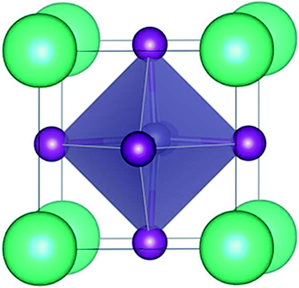 | ||
| Fig. 1 The crystal structure of CsGeI3. | ||
For the halide perovskite CsGeI3, by changing the lattice constant of the CsGeI3 structure, the structure was optimized to obtain a series of changes of energies, volumes, Ge–I–Ge bond angles, and Ge–I bond lengths. The detailed changes of these structural parameters are displayed in Fig. 2. It can be seen that the effects of strain have great impacts on the energies, volumes, Ge–I–Ge bond angles, and Ge–I bond lengths. Whether it is compressive or tensile strain, the stability of the structure is less than that of CsGeI3 without strain. Upon applying compressive (tensile) strain, the volume will decrease (increase). The Ge–I–Ge angles show a gradual reduction with the ε value ranging from −4% to 4%. The Ge–I bonds in CsGeI3 are divided into two kinds of bonds: short and long bonds. As shown in Fig. 2(d), the length of the short Ge–I bond remains unchanged, whereas that of the long Ge–I bond exhibits an evident increment with the ε value ranging from −4% to 4%. The change in the Ge–I–Ge angles and Ge–I bond lengths would significantly influence the electronic structures of CsGeI3.
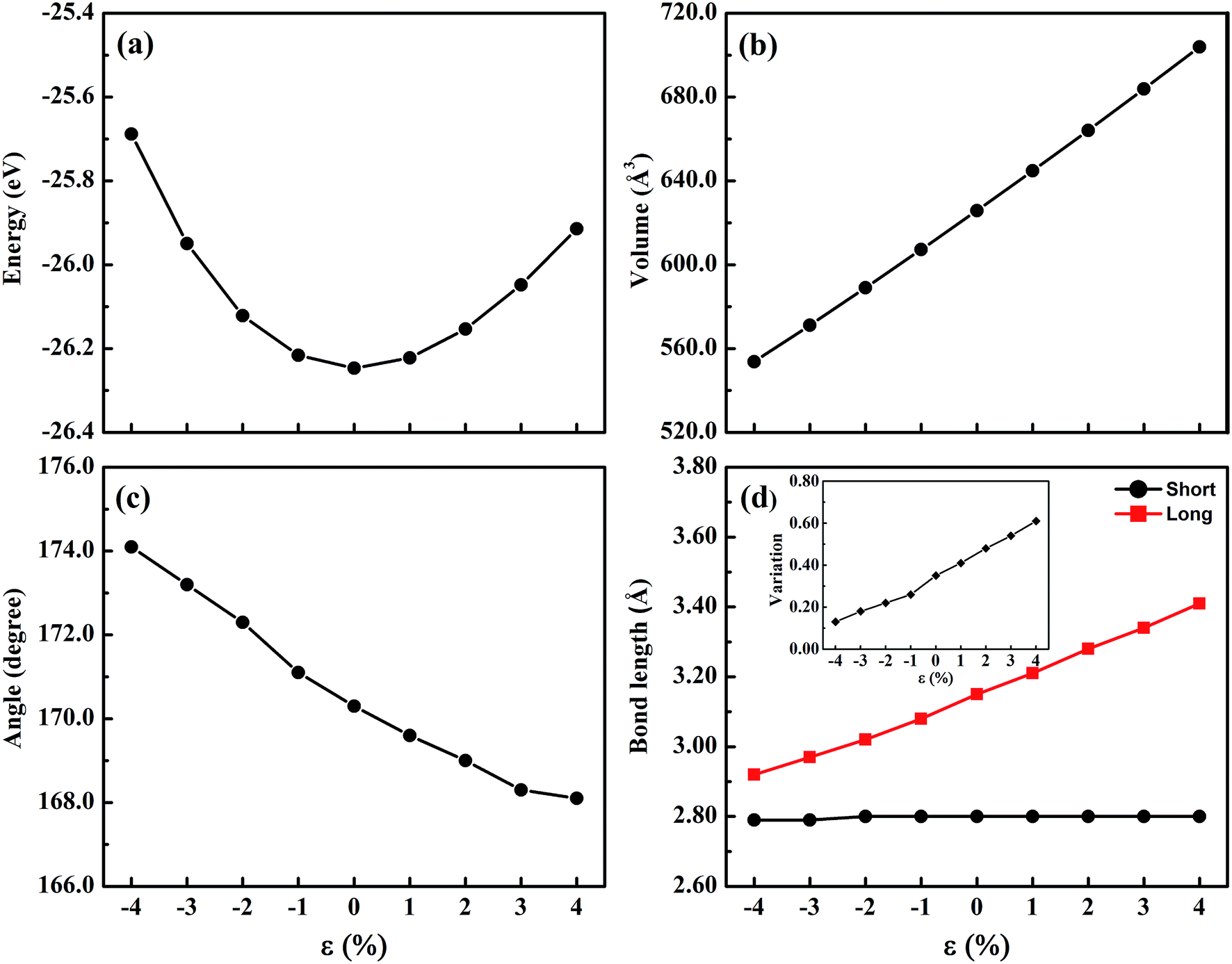 | ||
| Fig. 2 The structural parameters of CsGeI3 under different strain conditions. (a) The curve of energy. (b) The curve of volume. (c) The curve of the Ge–I–Ge angle. (d) The curve of the Ge–I bond length. The variation of the short and long Ge–I bond lengths is shown in the inset of (d). | ||
3.2 Electronic properties
To better explore the electronic properties of CsGeI3, we employed two DFT methods. The band gap of CsGeI3 is found to be 0.68 eV by PBE calculation, which agrees well with other theoretical results.45,46 However, this value is much smaller than the experimental results. To obtain more accurate band gap, we have used HSE06 calculation. The band structure of CsGeI3 is shown in Fig. 3. It can be seen that CsGeI3 is a direct bandgap semiconductor with a value of 1.56 eV, which is in good agreement with previous experimental results.35,44 The density of states (DOS) and partial DOS of CsGeI3 perovskite are presented in Fig. 3. Cs+ does not contribute to the band edge states because the states of Cs+ are far from the Fermi level. The valence band maximum (VBM) of CsGeI3 is mainly contributed by the I-5p orbital, whereas the conduction band minimum (CBM) is dominated by the Ge-4p orbital.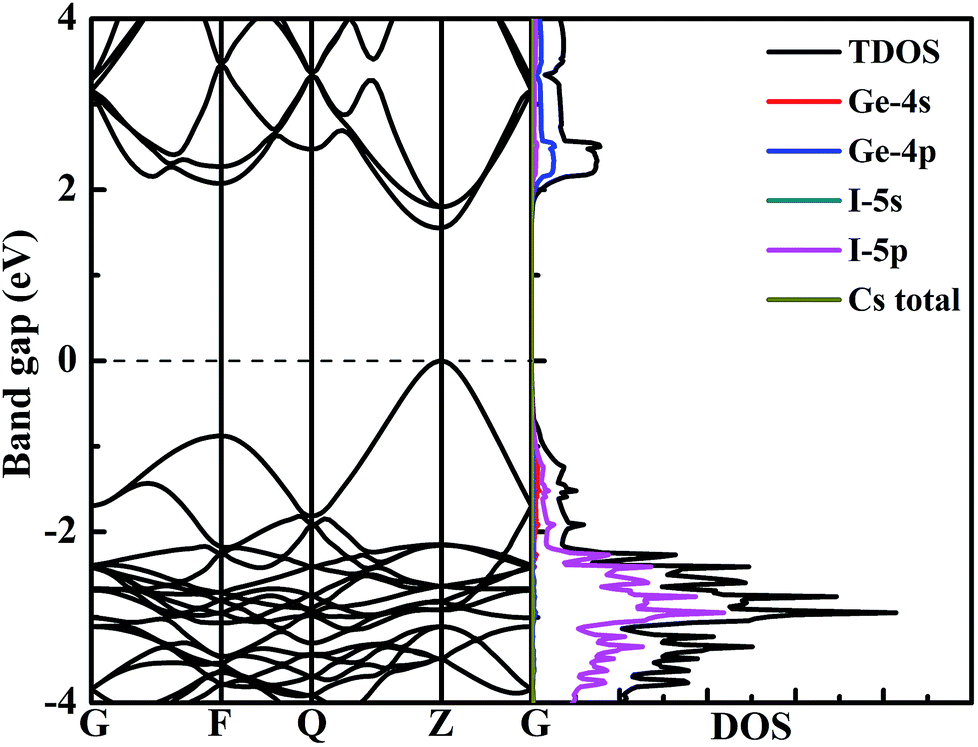 | ||
| Fig. 3 The band structure and density of states of CsGeI3 calculated at the HSE06 level. | ||
The effects of strain on the band gap of CsGeI3 were investigated. When strain was applied in the range from −4% to 4%, the band gaps of CsGeI3 tuned from 0.73 to 2.30 eV. Interestingly, CsGeI3 still remains a direct-bandgap semiconductor over the whole strain range. Both the CBM and VBM of CsGeI3 decrease when strain is applied in the range from −4% to 4%. The band gap of CsGeI3 with ε = −1% is 1.36 eV, which is in the range of 1.3–1.4 eV. It indicates that this structure will have the best photovoltaic performance under this condition according to the Shockley–Queisser theory.47 A suitable band gap can be obtained by applying a rather weak pressure (0.52 GPa). The band gaps of the CsGeI3 structure calculated at the PBE level show trends similar to those calculated at the HSE06 level, as shown in Fig. 4(a). The relationships between stress and strain for CsGeI3 under different conditions are shown in Fig. 4(b). It can be seen that the value of stress gradually decreases when ε increases from −4% to 4%.
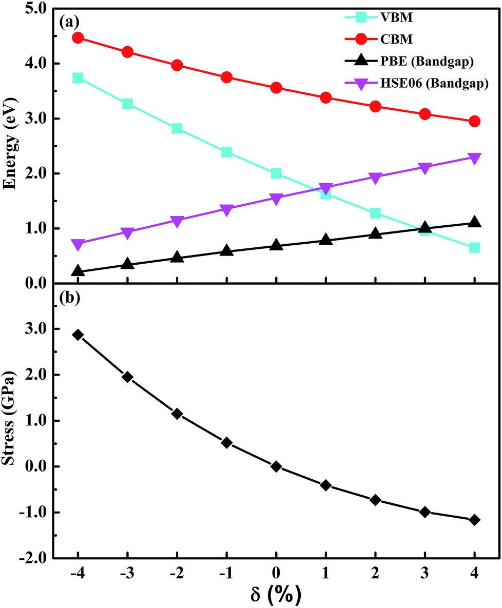 | ||
| Fig. 4 (a) VBM, CBM, bandgap and (b) stress of CsGeI3 as a function of strain. | ||
It is important to understand the reasons for the change in the band gap of CsGeI3 under strain. The response of the band gap under strain can be related with the geometry changes. A previous study has indicated that the electronic properties of hybrid perovskites are affected by structural distortion, and the main factor is the Pb–I–Pb bond angle.48 The Ge–I–Ge bond angles of CsGeI3 under different strain conditions are shown in Fig. 2(c). The smaller distortion of the Ge–I–Ge bond angle for CsGeI3 (ε = −4%) results in a smaller band gap of 0.73 eV when compared with that of CsGeI3 (1.56 eV) without strain. However, the slightly greater distortion of the Ge–I–Ge bond angle for CsGeI3 (ε = 4%) results in a higher band gap of 2.30 eV when compared with that of CsGeI3 without strain. It can be seen that the change in the Ge–I–Ge bond angles can provide an explanation for the difference in the band gap of CsGeI3 under different strain conditions.
We then mainly evaluated the stability of CsGeI3 under a strain of −1%. The elastic constants are essential to predict the mechanical stability of a crystal. The well-known stability criteria for a trigonal crystal is given by C11 − |C12| > 0, (C11 + C12)C33 > 2C132, (C11 − C12)C44 > 2C142.49 The calculated elastic constants satisfy the stability criteria; this implies that this compound is mechanically stable. In addition, the phonon spectrum of this compound has been studied and is shown in Fig. 5. None of the imaginary phonon mode exists in the calculated phonon spectra; this suggested that this compound is kinetically stable. Based on the abovementioned stability study, iCsGeI3 (ε = −1%) can be obtained under proper experimental conditions.
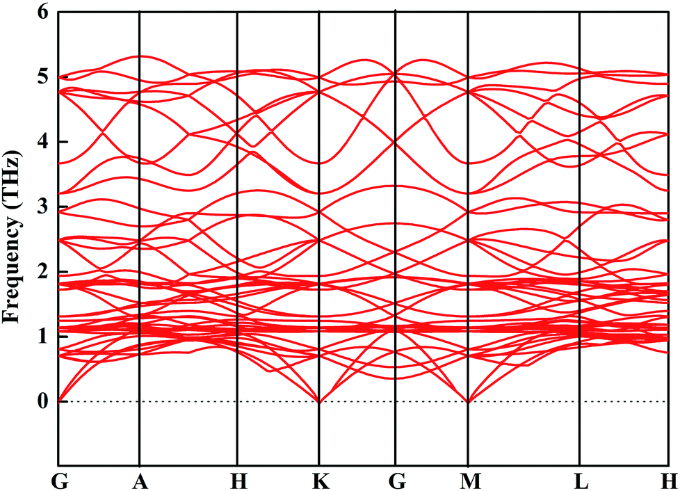 | ||
| Fig. 5 Phonon spectrum of CsGeI3 (ε = −1%). | ||
To estimate the amount of charge transfer between atoms due to the hydrostatic strain, we have calculated the Bader charges of CsGeI3 under different strain conditions. The results of the charge transfer are shown in Fig. 6. The Bader charges of Cs, Ge, and I ions fluctuate from 0.81 to 0.86e, 0.64 to 0.67e, and −0.48 to −0.51e, respectively. Compressive strain results in a decrease in the partial charges of Cs and Ge. On the contrary, tensile strain increases the values of the partial charges of Cs and Ge atoms. A similar change of the partial charges of I is also observed.
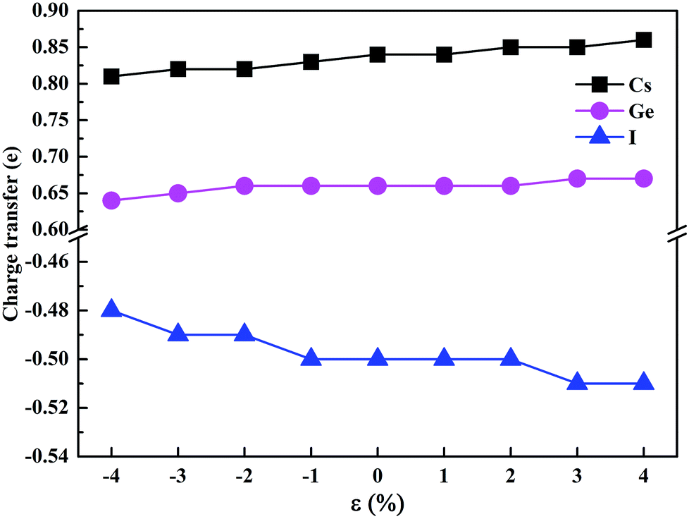 | ||
| Fig. 6 The charge transfer of the Cs, Ge, and I atoms. | ||
3.3 Optical properties
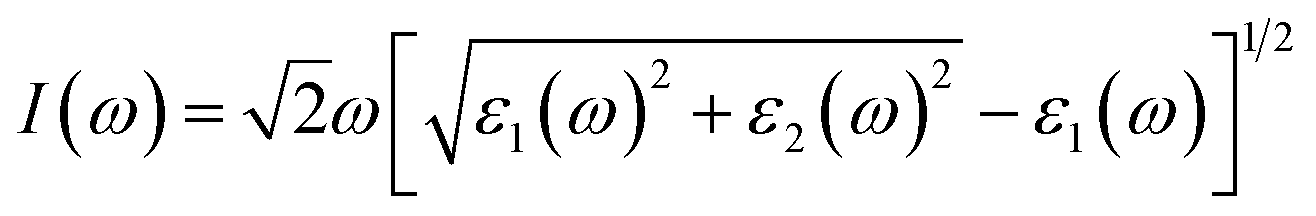
The investigation of the optical properties of materials is important to reveal the response of materials to light. Therefore, deep insights into the optical parameters are essential for the practical applications of materials in optoelectronic devices. To better understand the optical performance of CsGeI3 under different strain conditions, we further calculated the optical absorption coefficients in the visible spectrum. The absorption coefficient I(ω) was calculated from the dielectric function as below:50
 | (1) |
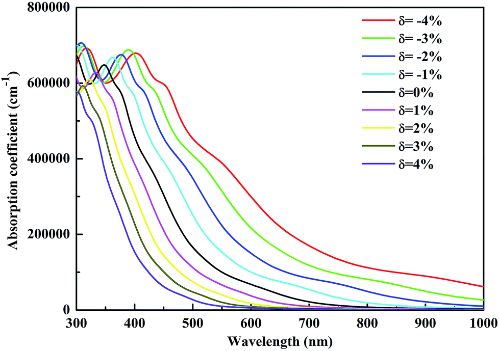 | ||
| Fig. 7 Calculated optical absorption coefficients of CsGeI3 under different strain conditions. | ||
4. Conclusion
In summary, we have systematically investigated the effects of strain on the structure, electronic and optical properties of CsGeI3 using the first-principles calculations. Our results show that the band gap of CsGeI3 can be tuned from 0.73 eV to 2.30 eV under different strain conditions. The results indicate that the change in the band gap under strain is likely to be determined by the Ge–I–Ge bond angle. The length of the short Ge–I bond remains unchanged, whereas that of the long Ge–I bond shows an evident increment with strain ranging from −4% to 4%. A suitable band gap (1.36 eV) is obtained upon applying a strain of −1%. Moreover, the CsGeI3 structure is predicted to be stable under this condition. Bandgap narrowing induces the redshift of the light absorption spectrum of CsGeI3 by extending the onset light absorption edge. Bandgap engineering by applying strain makes the halide perovskite CsGeI3 achieve a suitable band gap and optical absorption, and thus, CsGeI3 becomes a promising material for photovoltaic applications. Our results provide an efficient and clean approach to optimize the photovoltaic performance of the inorganic halide perovskite CsGeI3.Conflicts of interest
There are no conflicts to declare.Acknowledgements
This work was supported by the National Science Foundation of China (No. 21673240) and the Foreign Cooperation Project of Fujian Province (No. 2017I0019).References
- W. Nie, H. Tsai, R. Asadpour, J.-C. Blancon, A. J. Neukirch, G. Gupta, J. J. Crochet, M. Chhowalla, S. Tretiak, M. A. Alam, H.-L. Wang and A. D. Mohite, Science, 2015, 347, 522–525 CrossRef CAS PubMed.
- F. Hao, C. C. Stoumpos, D. H. Cao, R. P. H. Chang and M. G. Kanatzidis, Nat. Photonics, 2014, 8, 489 CAS.
- J. You, Z. Hong, Y. Yang, Q. Chen, M. Cai, T.-B. Song, C.-C. Chen, S. Lu, Y. Liu, H. Zhou and Y. Yang, ACS Nano, 2014, 8, 1674–1680 CrossRef CAS PubMed.
- J. H. Noh, S. H. Im, J. H. Heo, T. N. Mandal and S. I. Seok, Nano Lett., 2013, 13, 1764–1769 CAS.
- N. J. Jeon, J. H. Noh, W. S. Yang, Y. C. Kim, S. Ryu, J. Seo and S. I. Seok, Nature, 2015, 517, 476–480 CAS.
- H.-S. Kim, C.-R. Lee, J.-H. Im, K.-B. Lee, T. Moehl, A. Marchioro, S.-J. Moon, R. Humphry-Baker, J.-H. Yum, J. E. Moser, M. Grätzel and N.-G. Park, Sci. Rep., 2012, 2, 591 Search PubMed.
- D. Shi, V. Adinolfi, R. Comin, M. Yuan, E. Alarousu, A. Buin, Y. Chen, S. Hoogland, A. Rothenberger, K. Katsiev, Y. Losovyj, X. Zhang, P. A. Dowben, O. F. Mohammed, E. H. Sargent and O. M. Bakr, Science, 2015, 347, 519–522 CrossRef CAS PubMed.
- A. Kojima, K. Teshima, Y. Shirai and T. Miyasaka, J. Am. Chem. Soc., 2009, 131, 6050–6051 CAS.
- NREL, Best Research-Cell Efficiences chart, http://www.nrel.gov/pv/assets/images/efficiency-chart-20180716.jpg.
- Y. Jiao, F. Ma, G. Gao, H. Wang, J. Bell, T. Frauenheim and A. Du, RSC Adv., 2015, 5, 82346–82350 CAS.
- M. Lyu, J.-H. Yun, M. Cai, Y. Jiao, P. V. Bernhardt, M. Zhang, Q. Wang, A. Du, H. Wang, G. Liu and L. Wang, Nano Res., 2016, 9, 692–702 CAS.
- N. K. Noel, S. D. Stranks, A. Abate, C. Wehrenfennig, S. Guarnera, A.-A. Haghighirad, A. Sadhanala, G. E. Eperon, S. K. Pathak, M. B. Johnston, A. Petrozza, L. M. Herz and H. J. Snaith, Energy Environ. Sci., 2014, 7, 3061–3068 CAS.
- W. E. I. Sha, X. Ren, L. Chen and W. C. H. Choy, Appl. Phys. Lett., 2015, 106, 221104 CrossRef.
- Y.-Q. Zhao, B. Liu, Z.-L. Yu, D. Cao and M.-Q. Cai, Electrochim. Acta, 2017, 247, 891–898 CrossRef CAS.
- Y.-Q. Zhao, Q.-R. Ma, B. Liu, Z.-L. Yu and M.-Q. Cai, Phys. Chem. Chem. Phys., 2018, 20, 14718–14724 RSC.
- Y. Nagaoka, K. Hills-Kimball, R. Tan, R. Li, Z. Wang and O. Chen, Adv. Mater., 2017, 29, 1606666 CrossRef PubMed.
- A. Jaffe, Y. Lin, W. L. Mao and H. I. Karunadasa, J. Am. Chem. Soc., 2017, 139, 4330–4333 CrossRef CAS PubMed.
- Q. Li, S. Li, K. Wang, Z. Quan, Y. Meng and B. Zou, J. Phys. Chem. Lett., 2017, 8, 500–506 CrossRef CAS PubMed.
- P. Wang, J. Guan, D. T. K. Galeschuk, Y. Yao, C. F. He, S. Jiang, S. Zhang, Y. Liu, M. Jin, C. Jin and Y. Song, J. Phys. Chem. Lett., 2017, 8, 2119–2125 CrossRef CAS PubMed.
- L. Wang, K. Wang, G. Xiao, Q. Zeng and B. Zou, J. Phys. Chem. Lett., 2016, 7, 5273–5279 CrossRef CAS PubMed.
- L. Wang, K. Wang and B. Zou, J. Phys. Chem. Lett., 2016, 7, 2556–2562 CrossRef CAS PubMed.
- I. P. Swainson, M. G. Tucker, D. J. Wilson, B. Winkler and V. Milman, Chem. Mater., 2007, 19, 2401–2405 CrossRef CAS.
- A. Jaffe, Y. Lin, C. M. Beavers, J. Voss, W. L. Mao and H. I. Karunadasa, ACS Cent. Sci., 2016, 2, 201–209 CrossRef CAS PubMed.
- T. Ou, J. Yan, C. Xiao, W. Shen, C. Liu, X. Liu, Y. Han, Y. Ma and C. Gao, Nanoscale, 2016, 8, 11426–11431 RSC.
- M. Szafrański and A. Katrusiak, J. Phys. Chem. Lett., 2016, 7, 3458–3466 CrossRef PubMed.
- S. Jiang, Y. Fang, R. Li, H. Xiao, J. Crowley, C. Wang, T. J. White, W. A. Goddard, Z. Wang, T. Baikie and J. Fang, Angew. Chem., Int. Ed., 2016, 55, 6540–6544 CrossRef CAS PubMed.
- Y. Wang, X. Lü, W. Yang, T. Wen, L. Yang, X. Ren, L. Wang, Z. Lin and Y. Zhao, J. Am. Chem. Soc., 2015, 137, 11144–11149 CrossRef CAS PubMed.
- L. Zhang, Q. Zeng and K. Wang, J. Phys. Chem. Lett., 2017, 8, 3752–3758 CrossRef CAS PubMed.
- X. Lü, Y. Wang, C. C. Stoumpos, Q. Hu, X. Guo, H. Chen, L. Yang, J. S. Smith, W. Yang, Y. Zhao, H. Xu, M. G. Kanatzidis and Q. Jia, Adv. Mater., 2016, 28, 8663–8668 CrossRef PubMed.
- L. Zhang, W. Geng, C.-j. Tong, X. Chen, T. Cao and M. Chen, Sci. Rep., 2018, 8, 7760 CrossRef PubMed.
- S. Bonomi, I. Tredici, B. Albini, P. Galinetto, A. Rizzo, A. Listorti, U. A. Tamburini and L. Malavasi, Chem. Commun., 2018, 54, 13212–13215 RSC.
- G. Liu, L. Kong, P. Guo, C. C. Stoumpos, Q. Hu, Z. Liu, Z. Cai, D. J. Gosztola, H.-k. Mao, M. G. Kanatzidis and R. D. Schaller, ACS Energy Lett., 2017, 2, 2518–2524 CrossRef CAS.
- U. Schwarz, F. Wagner, K. Syassen and H. Hillebrecht, Phys. Rev. B: Condens. Matter Mater. Phys., 1996, 53, 12545–12548 CrossRef CAS.
- D. K. Seo, N. Gupta, M. H. Whangbo, H. Hillebrecht and G. Thiele, Inorg. Chem., 1998, 37, 407–410 CrossRef CAS PubMed.
- T. Krishnamoorthy, H. Ding, C. Yan, W. L. Leong, T. Baikie, Z. Zhang, M. Sherburne, S. Li, M. Asta, N. Mathews and S. G. Mhaisalkar, J. Mater. Chem. A, 2015, 3, 23829–23832 RSC.
- G. Kresse and J. Furthmüller, Comput. Mater. Sci., 1996, 6, 15–50 CAS.
- P. E. Blöchl, Phys. Rev. B: Condens. Matter Mater. Phys., 1994, 50, 17953–17979 CrossRef.
- J. P. Perdew, K. Burke and M. Ernzerhof, Phys. Rev. Lett., 1996, 77, 3865–3868 CrossRef CAS PubMed.
- J. Heyd, G. E. Scuseria and M. Ernzerhof, J. Chem. Phys., 2003, 118, 8207–8215 CrossRef CAS.
- J. Heyd, G. E. Scuseria and M. Ernzerhof, J. Chem. Phys., 2006, 124, 219906 CrossRef.
- J. P. Perdew, A. Ruzsinszky, G. I. Csonka, O. A. Vydrov, G. E. Scuseria, L. A. Constantin, X. Zhou and K. Burke, Phys. Rev. Lett., 2008, 100, 136406 CrossRef PubMed.
- J. Klimeš, D. R. Bowler and A. Michaelides, Phys. Rev. B: Condens. Matter Mater. Phys., 2011, 83, 195131 CrossRef.
- T. Thonhauser, V. R. Cooper, S. Li, A. Puzder, P. Hyldgaard and D. C. Langreth, Phys. Rev. B: Condens. Matter Mater. Phys., 2007, 76, 125112 CrossRef.
- C. C. Stoumpos, L. Frazer, D. J. Clark, Y. S. Kim, S. H. Rhim, A. J. Freeman, J. B. Ketterson, J. I. Jang and M. G. Kanatzidis, J. Am. Chem. Soc., 2015, 137, 6804–6819 CrossRef CAS PubMed.
- X. Lu, Z. Zhao, K. Li, Z. Han, S. Wei, C. Guo, S. Zhou, Z. Wu, W. Guo and C.-m. L. Wu, RSC Adv., 2016, 6, 86976–86981 RSC.
- J. Qian, B. Xu and W. Tian, Org. Electron., 2016, 37, 61–73 CrossRef CAS.
- W. Shockley and H. J. Queisser, J. Appl. Phys., 1961, 32, 510–519 CrossRef CAS.
- Z. Xiao, W. Meng, J. Wang, D. B. Mitzi and Y. Yan, Mater. Horiz., 2017, 4, 206–216 RSC.
- M. Born and K. Huang, Dynamical Theory of Crystal Lattices, Oxford University Press, Oxford, 1962 Search PubMed.
- S. Saha, T. P. Sinha and A. Mookerjee, Phys. Rev. B: Condens. Matter Mater. Phys., 2000, 62, 8828–8834 CrossRef CAS.
| This journal is © The Royal Society of Chemistry 2019 |